1
LT1176/LT1176-5
Step-Down
Switching Regulator
S
FEATURE
s
1.2A On-Board Switch
s
100kHz Switching Frequency
s
Excellent Dynamic Behavior
s
DIP and Surface Mount Packages
s
Only 8mA Quiescent Current
s
Preset 5V Output Available
s
Operates Up to 35V Input
s
Micropower Shutdown Mode
U
A
O
PPLICATI
TYPICAL
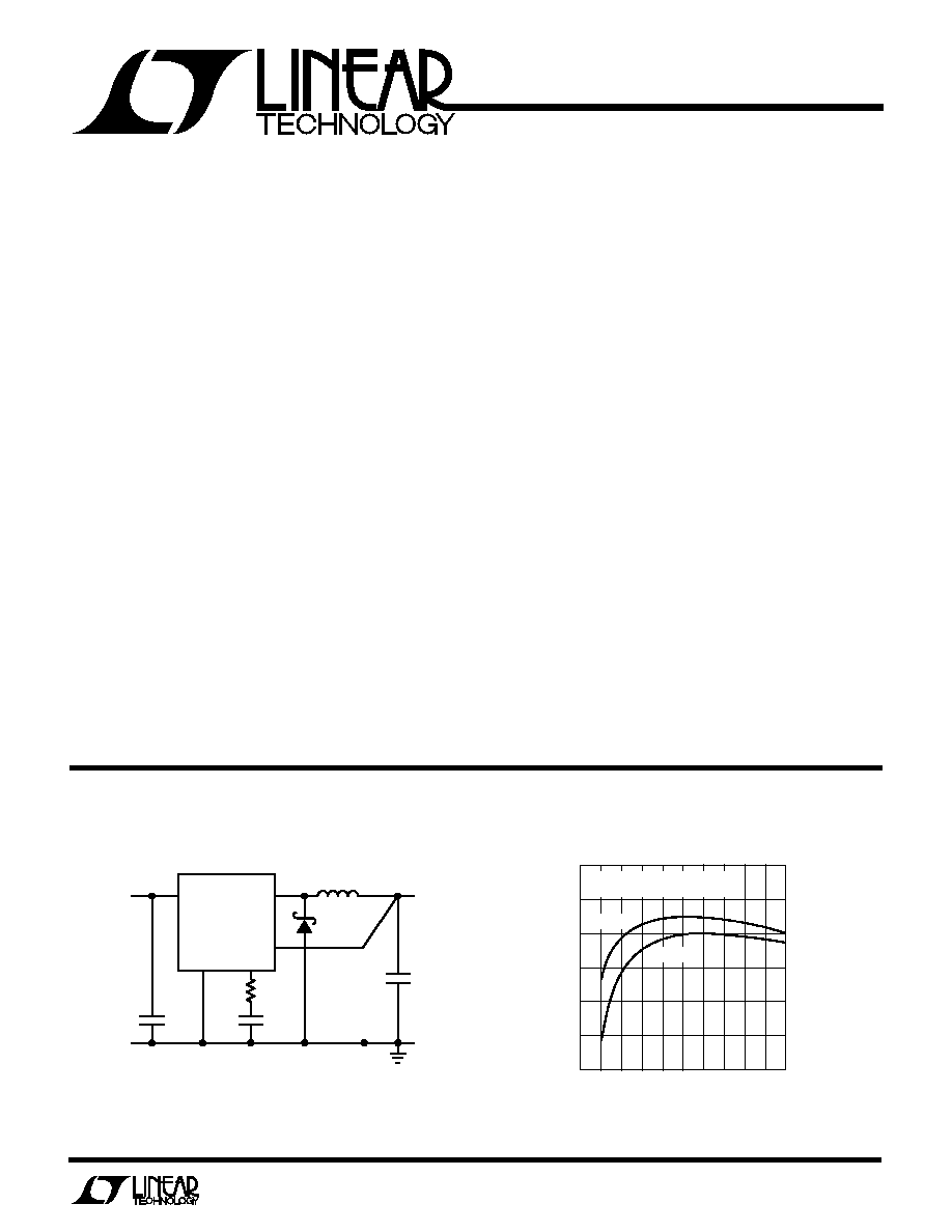
Basic 5V Positive Buck Converter
5V Buck Converter Efficiency
tion. The power switch, all oscillator and control circuitry,
and all current limit components are included on the chip.
The topology is a classic positive "buck" configuration but
several design innovations allows this device to be used as
a positive-to-negative converter, a negative boost con-
verter, and as a flyback converter. The switch output is
specified to swing below ground.
The LT1176 uses a true analog multiplier in the feedback
loop. This makes the device respond nearly instantaneously
to input voltage fluctuations and makes loop gain indepen-
dent of input voltage. As a result, dynamic behavior of the
regulator is significantly improved over previous designs.
On-chip pulse by pulse current limiting makes the LT1176
nearly bust-proof for output overloads or shorts. The input
voltage range as a buck converter is 8V to 35V, but a self-
boot feature allows input voltages as low as 5V in the
inverting and boost configurations.
The LT1176 is available in a low cost 8-lead DIP package
with frequency preset at 100kHz and current limit at 1.7A An
adjustable output is offered as well as a preset 5V version.
For further design details and application help, see the
LT1074/LT1076 data sheet and Application Note 44.
D
U
ESCRIPTIO
The LT1176 is a 1A monolithic bipolar switching regulator
which requires only a few external parts for normal opera-
U
S
A
O
PPLICATI
s
Buck Converter with Output Voltage Range of
2.5V to 30V
s
Positive-to-Negative Converter
s
Negative Boost Converter
s
Mulitple Output Buck Converter
V
C
GND
LT1176-5
R3
2.7k
C2
0.01
µ
F
1N5819
+
C3
100
µ
F
+
C1
470
µ
F
25V
LT1176/76-5 ∑ TA01
5V, 0.8A
10V T0 35V
L1*
100
µ
H
*COILTRONICS #100-1-52
PULSE ENGINEERING, INC. #PE-92102
HURRICANE #HL-AG210LL
THESE ARE LOW COST POWDERED IRON CORES. OPTIMUM EFFICIENCY
AND SMALLEST SIZE IS OBTAINED BY USING A LOW LOSS CORE SUCH
AS MAGNETICS INC. KOOL M
µ
. SEE EFFICIENCY GRAPH.
V
IN
V
SW
SENSE
LOAD CURRENT (A)
60
EFFICIENCY (%)
70
80
90
0.2
0.4
0.6
0.8
LT1176/76-5 ∑ TA02
1.0
0.1
0.3
0.5
0.7
0.9
L = 100
µ
H ON MAGNETICS INC.
SIZE T-50 KOOL M
µ
CORE
V
IN
= 20V
V
IN
= 10V
2
LT1176/LT1176-5
A
U
G
W
A
W
U
W
A
R
BSOLUTE
XI
TI
S
Input Voltage .......................................................... 38V
Switch Voltage With Respect to Input Voltage ........ 50V
Switch Voltage With Respect to Ground Pin
(V
SW
Negative) (Note 6) ......................................... 20V
Feedback Pin Voltage....................................... ≠ 2V, 10V
Shutdown Pin Voltage (Not to Exceed V
IN
) ............. 35V
Status Pin Voltage
(Current Must Be Limited to 5mA When Status Pin
Switches "ON") ................................................... 30V
I
LIM
Pin Voltage (Forced) ...................................... 5.5V
Maximum Operating Ambient Temperature Range
LT1176C/LT1176C-5 .............................. 0
∞
C to 70
∞
C
Maximum Operating Junction Temperature Range
LT1176C/LT1176C-5 ............................ 0
∞
C to 125
∞
C
Storage Temperature Range ................ ≠ 65
∞
C to 150
∞
C
Lead Temperature (Soldering, 10 sec) 300
∞
C
W
U
U
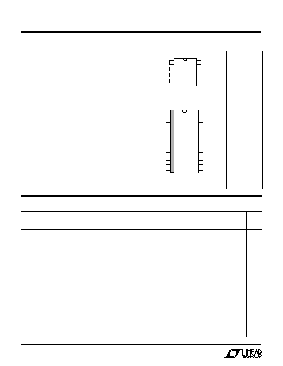
PACKAGE/ORDER I FOR ATIO
ORDER PART
NUMBER
1
2
3
4
8
7
6
5
TOP VIEW
V
IN
I
LIM
GND
FB/SENSE
V
SW
V
C
STATUS
SHUTDOWN
N8 PACKAGE
8-LEAD PLASTIC DIP
T
J MAX
= 125
∞
C,
JA
= 90
∞
C/ W*
T
JMAX
= 125
∞
C,
JA
= 50
∞
C/ W*
ORDER PART
NUMBER
LT1176CN8
LT1176CN8-5
ELECTRICAL C
C
HARA TERISTICS
T
J
= 25
∞
C, V
IN
= 25V, unless otherwise noted
PARAMETER
CONDITIONS
MIN
TYP
MAX
UNITS
Switch "ON" Voltage (Note 1)
I
SW
= 0.2A
q
1.1
V
I
SW
= 1A
q
1.4
V
Switch "OFF" Leakage
V
IN
= 25V, V
SW
= 0
150
µ
A
V
IN
= V
MAX
, V
SW
= 0 (Note 7)
250
µ
A
Supply Current (Note 2)
V
FB
= 2.5V, V
IN
35V
q
7.5
10
mA
V
SHDN
= 0.1V (Device Shutdown) (Note 8)
q
140.0
300
µ
A
Minimum Supply Voltage
Normal Mode
q
7.3
8.0
V
Startup Mode (Note 3)
q
3.5
4.8
V
Switch Current Limit (Note 4)
I
LIM
Open
q
1.2
1.7
2.2
A
R
LIM
= 10k (Note 5)
1.2
A
R
LIM
= 7k (Note 5)
0.8
A
Maximum Duty Cycle
q
85
90
%
Switching Frequency
90
100
110
kHz
q
85
120
kHz
V
FB
= 0V Through 2k (Note 4) (LT1176)
20
kHz
V
SENSE
= 0V (Note 4) (LT1176-5)
20
kHz
Switching Frequency Line Regulation
8V
V
IN
V
MAX
(Note 7)
q
0.03
0.1
%/ V
Error Amplifier Voltage Gain (Note 9)
1V
V
C
4V
2000
V/ V
Error Amplifier Transconductance (Note 9)
3700
5000
8000
µ
mho
Error Amplifier Source and Sink Current
Source (V
FB
= 2V or V
SENSE
= 4V)
100.0
140.0
225.0
µ
A
Sink (V
FB
= 2.5V or V
SENSE
= 5.5V)
0.7
1.0
1.6
mA
*These thermal resistance numbers are for typical mounting technique. Lower thermal resistance
can be obtained with large copper lands, thermal glues or heatsinks.
1
2
3
4
5
6
7
8
9
10
TOP VIEW
S PACKAGE
20-LEAD PLASTIC SOL
20
19
18
17
16
15
14
13
12
11
V
IN
NC
I
LIM
GND
GND
GND
GND
NC
FB/SENSE
NC
V
SW
NC
V
C
GND
GND
GND
GND
STATUS
SHUTDOWN
NC
LT1176CS
LT1176CS-5
3
LT1176/LT1176-5
PARAMETER
CONDITIONS
MIN
TYP
MAX
UNITS
Feedback Pin Bias Current (LT1176)
V
FB
= V
REF
q
0.5
2
µ
A
Reference Voltage (LT1176)
V
C
= 2V
q
2.155
2.21
2.265
V
Reference Voltage Tolerance (LT1176)
V
REF
(Nominal) = 2.21V
±
0.5
±
1.5
%
All Conditions of Input Voltage, Output
q
±
1.0
±
2.5
%
Voltage, Temperature and Load Current
Sense Voltage (LT1176-5)
V
C
= 2V
q
4.85
5
5.15
V
Sense Voltage Tolerance (LT1176-5)
V
OUT
(Nominal) = 5V
±
0.5
±
2
%
All Conditions of Input Voltage,
q
±
1.0
±
3
%
Temperature and Load Current
Sense Pin Divider Resistance (LT1176-5)
3
5
8
k
Output Voltage Line Regulation
8V
V
IN
V
MAX
(Note 7)
q
0.005
0.02
%/ V
V
C
Voltage at 0% Duty Cycle
1.5
V
Over Temperature
q
≠ 4.0
mV/
∞
C
Multiplier Reference Voltage
24
V
Shutdown Pin Current
V
SHDN
= 5V
q
5
10
20
µ
A
V
SHDN
V
THRESHOLD
(
2.5V)
q
50
µ
A
Shutdown Thresholds
Switch Duty Cycle = 0
q
2.2
2.45
2.7
V
Fully Shut Down
q
0.1
0.30
0.5
V
Status Window
As a Percent of Output Voltage
±
4
±
5
±
6
%
Status High Level
I
STATUS
= 10
µ
A Sourcing
q
3.5
4.5
5.0
V
Status Low Level
I
STATUS
= 1.6mA Sinking
q
0.25
0.4
V
Status Delay Time
9
µ
s
Status Minimum Width
30
µ
s
ELECTRICAL C
C
HARA TERISTICS
T
J
= 25
∞
C, V
IN
= 25V, unless otherwise noted
Information furnished by Linear Technology Corporation is believed to be accurate and reliable.
However, no responsibility is assumed for its use. Linear Technology Corporation makes no represen-
tation that the interconnection of its circuits as described herein will not infringe on existing patent rights.
The
q
denotes specifications which apply over the full operating tempera-
ture range.
Note 1: To calculate maximum switch "ON" voltage at current between low
and high conditions, a linear interpolation may be used.
Note 2: A feedback pin voltage (V
FB
) of 2.5V forces the V
C
pin to its low
clamp level and the switch duty cycle to zero. This approximates the zero
load condition where duty cycle approaches zero. The LT1176-5 has
V
SENSE
= 5.5V.
Note 3: Total voltage from V
IN
pin to ground pin must be
8V after start-
up for proper regulation.
Note 4: Switch frequency is internally scaled down when the feedback pin
voltage is less than 1.3V to avoid extremely short switch-on times. During
testing, V
FB
or V
SENSE
is adjusted to give a minimum switch-on time of 1
µ
s.
Note 5: I
LM
= (R
LIM
≠ 1k)/ 7.65k
Note 6: Switch to input voltage limitation must also be observed.
Note 7: V
MAX
= 35V
Note 8: Does not include switch leakage.
Note 9: Error amplifier voltage gain and transconductance are specified
relative to the internal feedback node. To calculate gain and transconduc-
tance from the sense pin (Output) to the V
C
pin on the LT1176-5, multiply
by 0.44.
Power = I
LOAD
(V
OUT
/V
IN
) + V
IN
[7mA + 3mA (V
OUT
/V
IN
) + 0.012 (I
LOAD
)]
I
PEAK
= I
LOAD(PEAK)
+ [V
OUT
(V
IN
≠ V
OUT
)]/2E
5
(V
IN
)(L)
Example: V
IN
= 15V, V
OUT
= 5V, I
LOAD
= 0.5A Continuous, 0.8A Peak,
L = 100
µ
H
Power (I
LOAD
= 0.5A) = 0.38W
I
PEAK
(I
LOAD
= 0.8A) = 0.97A
Where component size or height is critical, we suggest using solid
tantalum capacitors (singly or in parallel), but be sure to use units rated
for switching applications. Coiltronics is a good source for low profile
surface mount inductors and AVX makes high quality surface mount
tantalum capacitors. For further help, use Application Notes 19 and 44,
LTC's SwitcherCAD computer design program, and our knowledgeable
application department.
Application Hints
Although the LT1176 has a peak switch rating of 1.2A and a maximum duty
cycle of 85%, it must be used cautiously in applications which require high
switch current and high duty cycle simultaneously, to avoid excessive chip
temperature. Thermal resistance is 90
∞
C/W for the 8-pin DIP package and
50
∞
C/W for the 20-pin SO. This limits continuous chip power dissipation to
the 0.5W to 1W range. These numbers assume typical mounting techniques.
Extra or thick copper connected to the leads can reduce thermal resistance.
Bonding the package to the board or using a clip style heatsink can also help.
The following formulas will give chip power dissipation and peak switch
current for the standard buck converter. Note that surges less than 30
seconds do not need to be considered from a thermal standpoint, but for
proper regulation, they must not result in peak switch currents exceeding the
1.2A limit.

4
LT1176/LT1176-5
Linear Technology Corporation
1630 McCarthy Blvd., Milpitas, CA 95035-7487
(408) 432-1900
q
FAX
: (408) 434-0507
q
TELEX
: 499-3977
©
LINEAR TECHNOLOGY CORPORATION 1993
LT/GP 0393 10K REV 0
W
I
D AGRA
BLOCK
NOTE:
PIN 1 IDENT, NOTCH ON TOP AND CAVITIES ON THE BOTTOM OF PACKAGES ARE THE MANUFACTURING OPTIONS.
THE PART MAY BE SUPPLIED WITH OR WITHOUT ANY OF THE OPTIONS.
SEE
NOTE
0.496 ≠ 0.512
(12.598 ≠ 13.005)
20
19
18
17
16
15
14
13
1
2
3
4
5
6
7
8
0.394 ≠ 0.419
(10.007 ≠ 10.643)
9
10
11
12
0.037 ≠ 0.045
(0.940 ≠ 1.143)
0.004 ≠ 0.012
(0.102 ≠ 0.305)
0.093 ≠ 0.104
(2.362 ≠ 2.642)
0.050
(1.270)
TYP
0.014 ≠ 0.019
(0.356 ≠ 0.482)
TYP
0∞ ≠ 8∞ TYP
SEE NOTE
0.009 ≠ 0.013
(0.229 ≠ 0.330)
0.016 ≠ 0.050
(0.406 ≠ 1.270)
0.291 ≠ 0.299
(7.391 ≠ 7.595)
◊
45
∞
0.010 ≠ 0.029
(0.254 ≠ 0.737)
0.005
(0.127)
RAD MIN
PACKAGE DESCRIPTIO
U
Dimensions in inches (milimeters) unless otherwise noted.
N Package 8-Lead Plastic DIP
0.045 ± 0.015
(1.143 ± 0.381)
0.100 ± 0.010
(2.540 ± 0.254)
0.065
(1.651)
TYP
0.045 ≠ 0.065
(1.143 ≠ 1.651)
0.130 ± 0.005
(3.302 ± 0.127)
0.020
(0.508)
MIN
0.018 ± 0.003
(0.457 ± 0.076)
0.125
(3.175)
MIN
0.009 ≠ 0.015
(0.229 ≠ 0.381)
0.300 ≠ 0.320
(7.620 ≠ 8.128)
0.325
+0.025
≠0.015
+0.635
≠0.381
8.255
(
)
1
2
3
4
8
7
6
5
0.250 ± 0.010
(6.350 ± 0.254)
0.400
(10.160)
MAX
S Package 20-Lead Plastic SOL
2.35V
≠
+
µ
POWER
SHUTDOWN
≠
+
0.3V
SHUTDOWN
INPUT SUPPLY
CURRENT LIMIT
SHUTDOWN
6V
REGULATOR
AND BIAS
I
LIM
6V TO ALL
CIRCUITRY
320
µ
A
10
µ
A
4.5V
10k
≠
+
CURRENT LIMIT
COMP
C2
500
0.16
R
R/S
LATCH
R
S
Q
≠
+
100kHz
OSCILLATOR
FREQ SHIFT
SYNC
3V
P-P
ANALOG
MULTIPLIER
XYZ
Z
Y
X
V
IN
OUTPUT
VOLTAGE
MONITOR
STATUS
2.21V
2.8k
FB/SENSE
2.2k*
V
C
24V (EQUIVALENT)
400
SWITCH
OUTPUT
(V
SW
)
≠
+
A1
ERROR
AMP
C1
PULSE WIDTH
COMPARATOR
*CONNECTED ON 5V VERSION ONLY
LT1176/76-5 ∑ BD
G1