 | –≠–ª–µ–∫—Ç—Ä–æ–Ω–Ω—ã–π –∫–æ–º–ø–æ–Ω–µ–Ω—Ç: LT1181AI | –°–∫–∞—á–∞—Ç—å:  PDF PDF  ZIP ZIP |
1
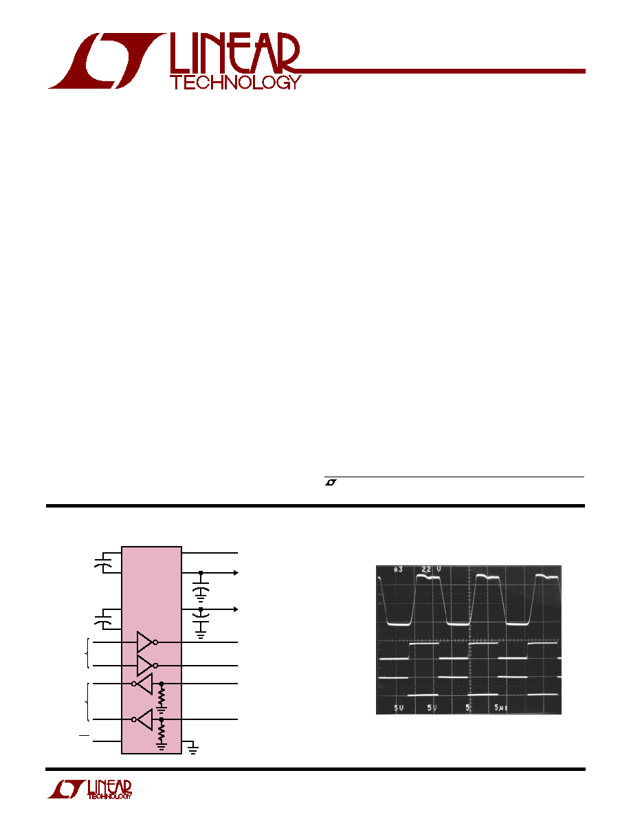
LT1180A/LT1181A
Low Power 5V RS232
Dual Driver/Receiver with
0.1
µ
F Capacitors
R
Output Waveforms
LT1180A ∑ TA02
DRIVER
OUTPUT
R
L
= 3k
C
L
= 2500pF
RECEIVER
OUTPUT
C
L
= 50pF
INPUT
U
A
O
PPLICATI
TYPICAL
5k
5k
0.1
µ
F
LOGIC
INPUTS
LOGIC
OUTPUTS
ON/OFF
18
10
13
11
12
6
5
4
2
16
9
14
8
15
7
3
17
5V INPUT
V
+
OUT
V
≠
OUT
RS232 OUTPUT
RS232 OUTPUT
RS232 INPUT
RS232 INPUT
LT1180A ∑ TA01
LT1180A
+
0.1
µ
F
+
0.1
µ
F
+
0.1
µ
F
+
s
ESD Protection over
±
10kV
s
Uses Small Capacitors: 0.1
µ
F
s
120kBaud Operation for R
L
= 3k, C
L
= 2500pF
s
250kBaud Operation for R
L
= 3k, C
L
= 1000pF
s
Outputs Withstand
±
30V Without Damage
s
CMOS Comparable Low Power: 40mW
s
Operates from a Single 5V Supply
s
Rugged Bipolar Design
s
Outputs Assume a High Impedance State When Off
or Powered Down
s
Meets All RS232 Specifications
s
Available With or Without Shutdown
s
Absolutely No Latch-up
s
Available in SO Package
S
FEATURE
D
U
ESCRIPTIO
s
Portable Computers
s
Battery-Powered Systems
s
Power Supply Generator
s
Terminals
s
Modems
U
S
A
O
PPLICATI
, LTC and LT are registered trademarks of Linear Technology Corporation.
TransZorb is a registered trademark of General Instruments, GSI
The LT
Æ
1180A/LT1181A are dual RS232 driver/receiver
pairs with integral charge pump to generate RS232 volt-
age levels from a single 5V supply. These circuits feature
rugged bipolar design to provide operating fault tolerance
and ESD protection unmatched by competing CMOS
designs. Using only 0.1
µ
F external capacitors, these cir-
cuits consume only 40mW of power, and can operate to
120k baud even while driving heavy capacitive loads. New
ESD structures on the chip allow the LT1180A/LT1181A to
survive multiple
±
10kV strikes, eliminating the need for
costly TransZorbs
Æ
on the RS232 line pins. The LT1180A/
LT1181A are fully compliant with EIA RS232 standards.
Driver outputs are protected from overload, and can be
shorted to ground or up to
±
30V without damage. During
shutdown or power-off conditions, driver and receiver
outputs are in a high impedance state, allowing line
sharing.
The LT1181A is available in 16-pin DIP and SO packages.
The LT1180A is supplied in 18-pin DIP and SO packages
for applications which require shutdown.
2
LT1180A/LT1181A
A
U
G
W
A
W
U
W
A
R
BSOLUTE
XI
TI
S
Supply Voltage (V
CC
) ................................................ 6V
V
+
........................................................................ 13.2V
V
≠
...................................................................... ≠13.2V
Input Voltage
Driver ........................................................... V
≠
to V
+
Receiver ............................................... ≠ 30V to 30V
ON/OFF ................................................. ≠ 0.3V to 12V
Output Voltage
Driver ...................................... V
+
≠ 30V to V
≠
+ 30V
Receiver .................................... ≠ 0.3V to V
CC
+ 0.3V
Short-Circuit Duration
V
+
................................................................... 30 sec
V
≠
................................................................... 30 sec
Driver Output .............................................. Indefinite
Receiver Output .......................................... Indefinite
Operating Temperature Range
LT1180AI/LT1181AI .......................... ≠ 40
∞
C to 85
∞
C
LT1180AC/LT1181AC ............................. 0
∞
C to 70
∞
C
Storage Temperature Range ................ ≠ 65
∞
C to 150
∞
C
Lead Temperature (Soldering, 10 sec)................. 300
∞
C
W
U
U
PACKAGE/ORDER I FOR ATIO
ORDER PART
NUMBER
ORDER PART
NUMBER
(Note 2)
ELECTRICAL C
C
HARA TERISTICS
PARAMETER
CONDITIONS
MIN
TYP
MAX
UNITS
Power Supply Generator
V
+
Output
7.9
V
V
≠
Output
≠ 7.0
V
Supply Current (V
CC
)
(Note 3), T
A
= 25
∞
C
9
13
mA
q
16
mA
Supply Current When OFF (V
CC
)
Shutdown (Note 4) LT1180A Only
q
1
10
µ
A
Supply Rise Time
C1 = C2 = C3 = C4 = 0.1
µ
F
0.2
ms
Shutdown to Turn-On
LT1180A Only
0.2
ms
ON/OFF Pin Thresholds
Input Low Level (Device Shutdown)
q
0.8
1.2
V
Input High Level (Device Enabled)
q
1.6
2.4
V
ON/OFF Pin Current
0V
V
ON/OFF
5V
q
≠ 15
80
µ
A
Oscillator Frequency
130
kHz
T
JMAX
= 150
∞
C,
JA
= 100
∞
C/ W,
JC
= 40
∞
C/W (J)
T
JMAX
= 125
∞
C,
JA
= 90
∞
C/ W,
JC
= 46
∞
C/W (N)
T
JMAX
= 125
∞
C,
JA
= 95
∞
C/ W,
JC
= 27
∞
C/W (SW)
LT1181ACN
LT1181ACSW
LT1181AIN
LT1181AISW
LT1181AMJ
LT1180ACN
LT1180ACSW
LT1180AIN
LT1180AISW
LT1180AMJ
T
JMAX
= 150
∞
C,
JA
=100
∞
C/ W,
JC
= 40
∞
C/W (J)
T
JMAX
= 125
∞
C,
JA
= 80
∞
C/ W,
JC
= 36
∞
C/W (N)
T
JMAX
= 125
∞
C,
JA
= 90
∞
C/ W,
JC
= 26
∞
C/W (SW)
1
2
3
4
5
6
7
8
9
TOP VIEW
18
17
16
15
14
13
12
11
10
NC
C1
+
V
+
C1
≠
C2
+
C2
≠
V
≠
TR2 OUT
REC2 IN
J PACKAGE
18-LEAD CERDIP
N PACKAGE
18-LEAD PDIP
ON/OFF
V
CC
GND
TR1 OUT
REC1 IN
REC1 OUT
TR1 IN
TR2 IN
REC2 OUT
SW PACKAGE
18-LEAD PLASTIC SO (WIDE)
1
2
3
4
5
6
7
8
TOP VIEW
16
15
14
13
12
11
10
9
C1
+
V
+
C1
≠
C2
+
C2
≠
V
≠
TR2 OUT
REC2 IN
V
CC
GND
TR1 OUT
REC1 IN
REC1 OUT
TR1 IN
TR2 IN
REC2 OUT
J PACKAGE
16-LEAD CERDIP
N PACKAGE
16-LEAD PDIP
SW PACKAGE
16-LEAD PLASTIC SO (WIDE)
(Note 1)
3
LT1180A/LT1181A
ELECTRICAL C
C
HARA TERISTICS
(Note 2)
The
q
denotes specifications which apply over the operating temperature
range (0
∞
C
T
A
70
∞
C for commercial grade, and ≠ 40
∞
C
T
A
85
∞
C for
industrial grade.
Note 1: Absolute Maximum Ratings are those values beyond which the life
of the device may be impaired.
Note 2: Testing done at V
CC
= 5V and V
ON/OFF
= 3V, unless otherwise
specified.
Note 3: Supply current is measured as the average over several charge
pump cycles. C
+
= C
≠
= C1 = C2 = 0.1
µ
F. All outputs are open, with all
driver inputs tied high.
Note 4: Supply current measurements in SHUTDOWN are performed with
V
ON/OFF
0.1V.
Note 5: For driver delay measurements, R
L
= 3k and C
L
= 51pF. Trigger
points are set between the driver's input logic threshold and the output
transition to the zero crossing (t
HL
= 1.4V to 0V and t
LH
= 1.4V to 0V).
Note 6: For receiver delay measurements, C
L
= 51pF. Trigger points are
set between the receiver's input logic threshold and the output transition
to standard TTL/CMOS logic threshold (t
HL
= 1.3V to 2.4V and t
LH
= 1.7V
to 0.8V).
Note 7: Data rate operation guaranteed by slew rate, short-circuit current
and propagation delay tests.
PARAMETER
CONDITIONS
MIN
TYP
MAX
UNITS
Driver
Output Voltage Swing
Load = 3k to GND
Positive
5.0
7.5
V
Negative
q
≠ 6.3
≠ 5.0
V
Logic Input Voltage Level
Input Low Level (V
OUT
= High)
q
1.4
0.8
V
Input High Level (V
OUT
= Low)
q
2.0
1.4
V
Logic Input Current
0.8V
V
IN
2.0V
q
5
20
µ
A
Output Short-Circuit Current
V
OUT
= 0V
±
9
17
mA
Output Leakage Current
Shutdown V
OUT
=
±
30V (Note 4)
q
10
100
µ
A
Date Rate (Note 7)
R
L
= 3k, C
L
= 2500pF
120
kBaud
R
L
= 3k, C
L
= 1000pF
250
kBaud
Slew Rate
R
L
= 3k, C
L
= 51pF
15
30
V/
µ
s
R
L
= 3k, C
L
= 2500pF
4
7
V/
µ
s
Propagation Delay
Output Transition t
HL
High-to-Low (Note 5)
0.6
1.3
µ
s
Output Transition t
LH
Low-to-High
0.5
1.3
µ
s
Receiver
Input Voltage Thresholds
Input Low Threshold (V
OUT
= High)
C Grade
q
0.8
1.3
V
Input High Threshold (V
OUT
= Low)
C Grade
q
1.7
2.4
V
Input Low
I, M Grade
q
0.2
1.3
V
Input High
I, M Grade
q
1.7
3.0
V
Hysteresis
q
0.1
0.4
1.0
V
Input Resistance
V
IN
=
±
10V
3
5
7
k
Output Leakage Current
Shutdown (Note 4) 0
V
OUT
V
CC
q
1
10
µ
A
Output Voltage
Output Low, I
OUT
= ≠ 1.6mA
q
0.2
0.4
V
Output High, I
OUT
= 160
µ
A (V
CC
= 5V)
q
3.5
4.2
V
Output Short-Circuit Current
Sinking Current, V
OUT
= V
CC
≠20
≠ 10
mA
Sourcing Current, V
OUT
= 0V
10
20
mA
Propagation Delay
Output Transition t
HL
High-to-Low (Note 6)
250
600
ns
Output Transition t
LH
Low-to-High
350
600
ns

4
LT1180A/LT1181A
C
C
HARA TERISTICS
U
W
A
TYPICAL PERFOR
CE
Receiver Input Thresholds
Supply Current
Driver Leakage in Shutdown
TEMPERATURE (∞C)
≠55
0.50
THRESHOLD VOLTAGE (V)
0.75
1.25
1.50
1.75
3.00
2.25
0
50
75
LT1180A ∑ TPC04
1.00
2.50
2.75
2.00
≠25
25
100
125
INPUT HIGH
INPUT LOW
Supply Current vs Data Rate
ON/OFF Thresholds
TEMPERATURE (∞C)
≠55
THRESHOLD VOLTAGE (V)
2.0
2.5
3.0
25
75
LT1180A ∑ TPC06
1.5
1.0
≠25
0
50
100
125
0.5
0
ON THRESHOLD
OFF THRESHOLD
TEMPERATURE (∞C)
0.1
LEAKAGE CURRENT (
µ
A)
10
100
LT1180A ∑ TPC08
1
≠55
0
50
75
≠25
25
100
125
V
OUT
= ≠30V
V
OUT
= 30V
Driver Short-Circuit Current
DATA RATE (kBAUD)
0
0
SUPPLY CURRENT (mA)
10
20
30
40
50
25
50
75
100
LT1180A ∑ TPC05
125
150
2 DRIVERS ACTIVE
R
L
= 3k
C
L
= 2500pF
TEMPERATURE (∞C)
≠55
0
SUPPLY CURRENT (mA)
10
25
0
50
75
LT1180A ∑ TPC07
5
20
15
≠25
25
100
125
2 DRIVERS LOADED R
L
= 3k
1 DRIVER LOADED R
L
= 3k
NO LOAD
Driver Output Voltage
Driver Maximum Output Voltage
vs Load Capacitance
TEMPERATURE (∞C)
≠55
≠10
DRIVER OUTPUT VOLTAGE (V)
≠8
≠4
≠2
0
10
4
0
50
75
LT1180A ∑ TPC03
≠6
6
8
2
≠25
25
100
125
OUTPUT HIGH
OUTPUT LOW
R
L
= 3k
V
CC
= 5V
V
CC
= 4.5V
V
CC
= 5.5V
V
CC
= 4.5V
V
CC
= 5V
V
CC
= 5.5V
LOAD CAPACITANCE (nF)
0
5.0
PEAK OUTPUT VOLTAGE (V)
5.5
6.0
6.5
7.0
7.5
8.0
2
4
6
8
LT1180A ∑ TPC01
10
1
3
5
7
9
20kBAUD
60kBAUD
120kBAUD
LOAD CAPACITANCE (nF)
0
≠7.0
PEAK OUTPUT VOLTAGE (V)
≠6.5
≠6.0
≠5.5
≠5.0
≠4.5
≠4.0
2
4
6
8
LT1180A ∑ TPC02
10
1
3
5
7
9
120kBAUD
60kBAUD
20kBAUD
Driver Minimum Output Voltage
vs Load Capacitance
TEMPERATURE (
∞
C)
≠55
SHORT-CIRCUIT CURRENT (mA)
20
25
30
25
75
LT1180A ∑ TPC09
15
10
≠25
0
50
100
125
5
0
I
SC
+
I
SC
≠
5
LT1180A/LT1181A
C
C
HARA TERISTICS
U
W
A
TYPICAL PERFOR
CE
LOAD CAPACITANCE (nF)
0
SLEW RATE (V/µs)
12
16
4.0
LT1180A ∑ TPC11
8
4
0
1.0
2.0
3.0
5.0
10
14
6
2
3.5
0.5
1.5
2.5
4.5
+SLEW
≠SLEW
LT1180A ∑ TPC13
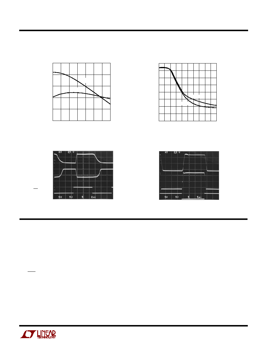
LT1180A ∑ TPC12
INPUT
DRIVER OUTPUT
R
L
= 3k
DRIVER OUTPUT
R
L
= 3k
C
L
= 2500pF
DRIVER 1
OUTPUT
ON/OFF PIN
Shutdown to Driver Outputs
Driver Output Waveforms
10V
5V
GND
GND
≠ 10V
≠ 5V
DRIVER 2
OUTPUT
Slew Rate vs Load Capacitance
Receiver Short-Circuit Current
PI FU CTIO S
U
U
U
V
+
: Positive Supply Output (RS232 Drivers). V
+
2V
CC
≠
1.5V. This pin requires an external charge storage capaci-
tor C
0.1
µ
F, tied to ground or V
CC
. Larger value capaci-
tors may be used to reduce supply ripple. With multiple
transceivers, the V
+
and V
≠
pins may be paralleled into
common capacitors.
V
≠
: Negative Supply Output (RS232 Drivers). V
≠
≠(2V
CC
≠ 2.5V). This pin requires an external charge storage
capacitor C
0.1
µ
F. Larger value capacitors may be used
to reduce supply ripple. With multiple transceivers, the V
+
and V
≠
pins may be paralleled into common capacitors.
TEMPERATURE (
∞
C)
≠55
0
SHORT-CIRCUIT CURRENT (mA)
20
50
0
50
75
LT1180A ∑ TPC10
10
40
30
≠25
25
100
125
RX I
SC
≠
RX I
SC
+
V
CC
: 5V Input Supply Pin. This pin should be decoupled
with a 0.1
µ
F ceramic capacitor close to the package pin.
Insufficient supply bypassing can result in low output
drive levels and erratic charge pump operation.
GND: Ground Pin.
ON/OFF: A TTL/CMOS Compatible Operating Mode Con-
trol. A logic low puts the LT1180A in shutdown mode.
Supply current drops to zero and both driver and receiver
outputs assume a high impedance state. A logic high fully
enables the device.