 | –≠–ª–µ–∫—Ç—Ä–æ–Ω–Ω—ã–π –∫–æ–º–ø–æ–Ω–µ–Ω—Ç: LT1182 | –°–∫–∞—á–∞—Ç—å:  PDF PDF  ZIP ZIP |
LT1768
1
The LT
Æ
1768 is designed to control single or multiple cold
cathode fluorescent lamp (CCFL) displays. A unique Mul-
timode Dimming scheme* combines both linear and PWM
control functions to maximize lamp life, efficiency, and
dimming range. Accurate maximum and minimum lamp
currents can be easily set. The LT1768 can detect and
protect against lamp failures and overvoltage start-up
conditions. It is designed to provide maximum flexibility
with a minimum number of external components.
The LT1768 is a current mode PWM controller with a 1.5A
MOSFET driver for high power applications. It contains a
350kHz oscillator, 5V reference, and a current sense
comparator with a 100mV threshold. It operates from an
8V to 24V input voltage. The LT1768 also has undervoltage
lockout, thermal limit, and a shutdown pin that reduces
supply current to 65
µ
A. It is available in a small 16-lead
SSOP package.
s
Ultrawide Multimode Dimming
TM
Range
s
Multiple Lamp Capability
s
Programmable PWM Dimming Range and
Frequency
s
Precision Maximum and Minimum Lamp
Currents Maximize Lamp Lifetime
s
No Lamp Flicker Under All Supply and Load
Conditions
s
Open Lamp Detection and Protection
s
350kHz Switching Frequency
s
1.5A MOSFET Gate Driver
s
100mV Current Sense Threshold
s
5V Reference Voltage Output
s
The 16-Lead SSOP Package
High Power CCFL Controller
for Wide Dimming Range and
Maximum Lamp Lifetime
s
Desktop Flat Panel Displays
s
Multiple Lamp Displays
s
Notebook LCD Displays
s
Point of Sale Terminal Displays
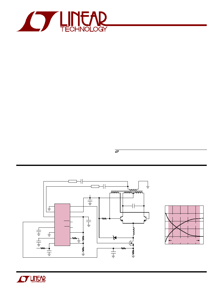
Figure 1. 14W CCFL Supply Produces a 100:1 Dimming Ratio While
Maintaining Minimum and Maximum Lamp Current Specifications
1768 TA01
C4
0.33
µ
F
250
1/4W
R5*
0.025
Q1
Q1
L1
68
µ
H
T1
33pF
33pF
0.1
µ
F
C1
33
µ
F
Si3456DY
MBRS130T3
LAMP
LAMP
R3
60.4k
R1
49.9k
R2
40.2k
R4
16.2k
C3
0.1
µ
F
C4
10
µ
F
C2
0.033
µ
F
V
IN
8V ≠ 24V
PROG
0V TO 5V OR
1kHz PWM
LT1768
DI02
PGND
GATE
V
C
AGND
C
T
PROG
DI01
SENSE
SHDN
R
MIN
R
MAX
PWM
FAULT
V
REF
V
IN
5V
2200pF
100
6
10
4
5
3
2
1
C4-WIMA MKP2
L1-COILTRONICS UP4-680
T1-2 CTX110607 IN PARALLEL
Q1-ZDT1048
*R5 CAN BE METAL PCB TRACE
LAMP CURRENT (mA)
0
10000
1000
100
10
1
0.1
8
1768 TA01b
2
4
6
10
DIMMING RATIO (NITS/NITS)
LAMP OUTPUT (NITS)
LAMP MANUFACTURERS
SPECIFIED CURRENT RANGE
Lamp Output and Dimming
Ratio vs Lamp Current
APPLICATIO S
U
FEATURES
TYPICAL APPLICATIO
U
DESCRIPTIO
U
, LTC and LT are registered trademarks of Linear Technology Corporation.
Multimode Dimming is a trademark of Linear Technology Corporation.
*Patent Pending

LT1768
2
SYMBOL
PARAMETER
CONDITIONS
MIN
TYP
MAX
UNITS
I
Q
Supply Current
9V< V
VIN
< 24V
q
7
8
mA
I
SHDN
Supply Current in Shutdown
V
SHDN
= 0V
q
65
100
µ
A
SHDN Pin Pull-Up Current
V
SHDN
= 0V
q
4
7
12
µ
A
SHDN Threshold Voltage
V
SHDN
Off to On
q
0.6
1.26
1.8
V
SHDN Threshold Hysteresis
q
100
200
300
mV
V
IN
Undervoltage Lockout
V
IN
Off to On
q
7.2
7.9
8.2
V
V
IN
Undervoltage Lockout
V
IN
On to Off
q
7.1
7.4
7.6
V
V
REF
REF Voltage
I
REF
= ≠1mA
q
4.9
5
5.1
V
REF Line Regulation
V
VIN
8V to 24V I
REF
= ≠1mA
q
7
20
mV
REF Load Regulation
I
REF
≠1mA to ≠10mA
q
10
20
mV
V
RMAX
R
MAX
Pin Voltage
q
1.225
1.25
1.275
V
V
RMIN
R
MIN
Pin Voltage
q
1.22
1.26
1.30
V
FSW
Switching Frequency
V
PROG
= 0.75V, V
SENSE
= 0V
q
300
350
410
kHz
Maximum Duty Cycle
V
PROG
= 0.75V, V
SENSE
= 0V
93
%
Minimum ON Time
V
PROG
= 0.75V, V
SENSE
= 150mV
125
ns
I
PROG
PROG Pin Input Bias Current
V
PROG
= 5V
q
100
500
nA
V
PROG
PROG Pin Voltage for Zero Lamp Current
(Note 2)
q
0.45
0.5
0.55
V
PROG Pin Voltage for Minimum Lamp Current
(Note 3)
q
0.9
1
1.1
V
PROG Pin Voltage for Maximum Lamp Current
(Note 4)
q
3.8
4
4.2
V
Input Voltage (V
IN
Pin) ............................................ 28V
SHDN Pin Voltage .................................................... 28V
FAULT Pin Voltage ................................................... 28V
PROG Pin Voltage ................................................... 5.5V
PWM Pin Voltage .................................................... 4.5V
C
T
Pin Voltage ........................................................ 4.5V
SENSE Pin Voltage .................................................... 1V
DIO1, DIO2 Input Current ...................................
±
50mA
R
MAX
Pin Source Current ..................................... 750
µ
A
R
MIN
Pin Source Current ..................................... 750
µ
A
V
REF
Pin Source Current ....................................... 10mA
Operating Junction Temperature Range
LT1768C ................................................ 0
∞
C to 125
∞
C
LT1768I ............................................ ≠ 40
∞
C to 125
∞
C
Storage Temperature Range ................. ≠ 65
∞
C to 150
∞
C
Lead Temperature (Soldering 10 sec)................... 300
∞
C
ORDER PART
NUMBER
Consult LTC Marketing for parts specified with wider operating temperature ranges.
ABSOLUTE AXI U
RATI GS
W
W
W
U
PACKAGE/ORDER I FOR ATIO
U
U
W
(Note 1)
ELECTRICAL CHARACTERISTICS
T
JMAX
= 125
∞
C,
JA
= 100
∞
C/W
1
2
3
4
5
6
7
8
TOP VIEW
GN PACKAGE
16-LEAD PLASTIC SSOP
16
15
14
13
12
11
10
9
PGND
DI01
DI02
SENSE
VC
AGND
C
T
PROG
GATE
V
IN
V
REF
FAULT
SHDN
R
MIN
R
MAX
PWM
LT1768CGN
LT1768IGN
The
q
denotes the specifications which apply over the full operating
temperature range, otherwise specifications are at T
A
= 25
∞
C, V
VIN
= 12V, I
DIO1/2
= 250
µ
A, V
PROG
= 0V, V
PWM
= 2.5V, I
RMAX
= ≠100
µ
A,
I
RMIN
= ≠100
µ
A, unless otherwise specified.
GN PART
MARKING
1768
1768I

LT1768
3
ELECTRICAL CHARACTERISTICS
SYMBOL
PARAMETER
CONDITIONS
MIN
TYP
MAX
UNITS
I
PWM
PWM Input Bias Current
q
0.6
4
µ
A
PWM Duty Cycle
V
PROG
= 1.75
45
50
55
%
PWM Frequency
C
T
= 0.22
µ
F (Note 7)
90
110
130
Hz
V
DIO1/2
DIO1/2 Positive Voltage
I
DIO
= 14mA
1.7
1.9
V
DIO1/2 Negative Voltage
I
DIO
= ≠14mA
≠1.1
≠1.3
V
V
VCCLAMP
VC High Clamp Voltage
V
PROG
= 4.5V (Note 8)
3.6
3.7
3.9
V
VC Switching Threshold
V
PROG
= 4.5V (Note 8)
0.5
0.7
0.95
V
I
SENSE
SENSE Input Bias Current
V
SENSE
= 0V
≠25
≠30
µ
A
V
SENSE
SENSE Threshold for Current Limit
V
VC
= V
VCCLAMP
, Duty Cycle < 50%, V
PROG
= 1V
85
100
115
mV
V
VC
= V
VCCLAMP
, Duty Cycle 80%, V
PROG
= 1V
90
mV
I
DIO1/2
to I
RMAX
Ratio
V
PROG
= 4.5V (Note 5)
q
94
98
104
A/A
V
PROG
= 4.5V, I
DIO1
or I
DIO2
= 0, V
VC
= 2.5V,
(Note 5)
45
49
55
A/A
I
DIO1/2
to I
RMIN
Ratio
V
PROG
< 0.75V (Note 6)
q
9
10
11
A/A
V
PROG
< 0.75V, I
DIO1
or I
DIO2
= 0, V
VC
= 2.5V,
(Note 6)
9
10
11
A/A
I
GATE
GATE Drive Peak Source Current
1.5
A
GATE Drive Peak Sink Current
1.5
A
GATE Drive Saturation Voltage
V
VIN
= 12V, I
GATE
= ≠100mA, V
PROG
= 4.5V
q
9.8
10.2
V
GATE Drive Clamp Voltage
V
VIN
= 24V, I
GATE
= ≠10mA, V
PROG
= 4.5V
q
12.5
14
V
GATE Drive Low Saturation Voltage
I
GATE
= 100mA
q
0.4
0.6
V
Open LAMP Threshold
(Note 9)
100
125
150
µ
A
FAULT Pin Saturation Voltage
I
FAULT
= 1mA, I
DI01
, I
DI02
= 0
µ
A, V
PROG
= 4.5V
0.2
0.3
V
FAULT Pin Leakage Current
V
FAULT
= 5V
20
100
nA
Thermal ShutdownTemperature
160
∞
C
Note 1: Absolute Maximum Ratings are those values beyond which the life
of a device may be impaired.
Note 2: This is the threshold voltage where the lamp current switches
from zero current to minimum lamp current. For V
PROG
less than the
threshold voltage, lamp current will be at zero. For V
PROG
greater than the
threshold voltage, lamp current will be equal to the minimum lamp
current. Minimum lamp current is set by the value of the resistor from the
R
MIN
pin to ground. See Applications Information for more details.
Note 3: This is the threshold voltage where the device starts to pulse width
modulate the lamp current. For V
PROG
less than the threshold voltage,
lamp current will be equal to the minimum lamp current. For V
PROG
greater than the threshold voltage, lamp current will be pulse width
modulated between the minimum lamp current and some higher value.
Minimum lamp current is set by the value of the resistor from the R
MIN
pin
to ground. The higher value lamp current is a function of the R
MAX
resistor
to ground value, and the voltages on the PWM and PROG pins. See
Applications Information for more details.
Note 4: This is the threshold voltage where the lamp current reaches its
maximum value. For V
PROG
greater than the threshold voltage, there will
be no increase in lamp current. For V
PROG
less than the threshold voltage,
lamp current will be at some lower value. Maximum lamp current is set by
The
q
denotes the specifications which apply over the full operating
temperature range, otherwise specifications are at T
A
= 25
∞
C, V
VIN
= 12V, I
DIO1/2
= 250
µ
A, V
PROG
= 0V, V
PWM
= 2.5V, I
RMAX
= ≠100
µ
A,
I
RMIN
= ≠100
µ
A, unless otherwise specified.
the value of the resistor from the R
MAX
pin to ground. The lower value
lamp current is a function of the R
MIN
and R
MAX
resistors, and the
voltages on the PWM and PROG pins. See Applications Information for
more details.
Note 5: I
DIO1/2
to I
RMAX
ratio is determined by setting I
RMAX
to ≠100
µ
A,
V
PROG
to 4.5V, V
VC
to 2.5V, and then ramping a DC current out of the
DIO1/2 pins from zero until the DC current in the VC voltage source
current equals zero. The I
DIO1/2
to I
RMAX
ratio is then defined as (I
DIO1
+
I
DIO2
)/I
RMAX
. See Applications Information for more details.
Note 6: I
DIO1/2
to I
RMIN
ratio is determined by setting I
RMIN
to ≠100
µ
A,
V
PROG
to 0.75V, V
VC
to 2.5V, and then ramping a DC current out of the
DIO1/2 pins from zero until the DC current in the VC voltage source
current equals zero. The I
DIO1/2
to I
RMIN
ratio is then defined as (I
DIO1
+
I
DIO2
)/I
RMIN
. See Applications Information for more details.
Note 7: The PWM frequency is set by the equation PWMFREQ = 22Hz/
C
T
(
µ
F).
Note 8: For VC voltages less than the switching threshold, GATE switching
is disabled.
Note 9: An open lamp will be detected if either I
DIO1
or I
DIO2
is less than
the threshold current for at least 1 full PWM cycle.

LT1768
4
TYPICAL PERFOR A CE CHARACTERISTICS
U
W
TEMPERATURE (
∞
C)
5.10
5.08
5.06
5.04
5.02
5.00
4.98
4.96
4.94
4.92
4.90
V
REF
VOLTAGE (V)
1768 G01
≠50
≠25
0
25
50
75
100
125
I
REF
= ≠1mA
TEMPERATURE (
∞
C)
1.30
1.29
1.28
1.27
1.26
1.25
1.24
1.23
1.22
1.21
1.20
VOLTAGE (V)
1768 G02
≠50
≠25
0
25
50
75
100
125
V
RMIN(V)
V
RMAX(V)
I
RMIN
= ≠100
µ
A
I
RMAX
= ≠100
µ
A
TEMPERATURE (
∞
C)
80
76
72
68
64
60
56
52
48
44
40
SHUTDOWN CURRENT (
µ
A)
1768 G03
≠50
≠25
0
25
50
75
100
125
V
SHDN
= 0V
INPUT VOLTAGE (V)
10
8
6
4
2
0
SUPPLY CURRENT (mA)
1768 G04
0
5
10
15
20
25
V
RMIN
, V
RMAX
vs Temperature
Supply Current in Shutdown vs
Temperature
Supply Current vs Input Voltage
V
REF
vs Temperature
TEMPERATURE (
∞
C)
7.40
7.30
7.20
7.10
7.00
6.90
6.80
6.70
6.60
6.50
6.40
SUPPLY CURRENT (mA)
1768 G05
≠50
≠25
0
25
50
75
100
125
INPUT VOLTAGE (V)
100
80
60
40
20
0
SHUTDOWN CURRENT (
µ
A)
1768 G06
0
5
10
15
20
25
V
SHDN
= 0V
TEMPERATURE (
∞
C)
2.00
1.80
1.60
1.40
1.20
1.00
0.80
0.60
0.40
0.20
0
SHUTDOWN VOLTAGE (V)
1768 G08
≠50
≠25
0
25
50
75
100
125
V
SHDN
ON TO OFF
V
SHDN
OFF TO ON
Supply Current vs Temperature
Supply Current in Shutdown vs
Input Voltage
Undervoltage Lockout Threshold
vs Temperature
SHDN Pull-Up Current
vs Input Voltage
Shutdown Threshold Voltage vs
Temperature
TEMPERATURE (
∞
C)
8.20
8.10
8.00
7.90
7.80
7.70
7.60
7.50
7.40
7.30
7.20
UNDERVOLTAGE LOCKOUT (V)
1768 G09
≠50
≠25
0
25
50
75
100
125
V
UVL
ON TO OFF
V
UVL
OFF TO ON
INPUT VOLTAGE (V)
0
SHDN PULL-UP CURRENT (
µ
A)
10
8
6
4
2
0
20
1768 G07
5
10
15
25
V
SHDN
= 0V

LT1768
5
TYPICAL PERFOR A CE CHARACTERISTICS
U
W
Switching Frequency vs Temperature
TEMPERATURE (
∞
C)
400
390
380
370
360
350
340
330
320
310
300
SWITCHING FREQUENCY (kHz)
1768 G10
≠50
≠25
0
25
50
75
100
125
TEMPERATURE (
∞
C)
124
120
116
112
108
104
100
96
92
88
84
PWM FREQUENCY (Hz)
1768 G11
≠50
≠25
0
25
50
75
100
125
C
T
= 0.22
µ
F
V
PWM
= 2.5V
TEMPERATURE (
∞
C)
0.250
0.225
0.200
0.175
0.150
0.125
0.100
0.75
0.50
0.25
0
FAULT VOLTAGE (V)
1768 G12
≠50
≠25
0
25
50
75
100
125
I
DIO1
= 0
µ
A
I
DIO2
= 0
µ
A
I
FAULT
= 1mA
I
FAULT
(mA)
0
450
400
350
300
250
200
150
100
1.5
2.5
1768
G13
0.5
1.0
2.0
3.0
3.5
FAULT VOLTAGE (mV)
I
DIO1
= 0
µ
A
I
DIO2
= 0
µ
A
TEMPERATURE (
∞
C)
50
45
40
35
30
25
20
15
10
5
0
SENSE CURRENT (
µ
A)
1768 G14
≠50
≠25
0
25
50
75
100
125
V
SENSE
= 0V
TEMPERATURE (
∞
C)
15.00
14.50
14.00
13.50
13.00
12.50
12.00
11.50
11.00
10.50
10.00
GATE CLAMP VOLTAGE (V)
1768 G15
≠50
≠25
0
25
50
75
100
125
I
GATE
= ≠10mA
V
IN
= 24V
V
IN
= 12V
FAULT Pin Saturation Voltage vs
Current
Maximum Gate Voltage vs
Temperature
Sense Pin Bias Current vs
Temperature
PWM Frequency vs Temperature
FAULT Pin Saturation Voltage vs
Temperature
DIO CURRENT (mA)
2.0
1.8
1.6
1.4
1.2
1.0
0.8
0.6
0.4
0.2
0
DIO VOLTAGE (V)
1768 G24
2
4
6
8
10
12 14 16
18 20
0
V
C
CURRENT (
µ
A)
3.75
3.74
3.73
3.72
3.71
3.70
3.69
3.68
3.67
3.66
3.65
V
C
CLAMP VOLTAGE (V)
1768 G25
0
50 100 150 200 250 300 350 400 450 500
VC Clamp Voltage vs Current
DIO Pin Voltage vs Current
DIO CURRENT (mA)
≠ 2.0
≠1.8
≠1.6
≠1.4
≠1.2
≠1.0
≠ 0.8
≠ 0.6
≠ 0.4
≠ 0.2
0
DIO VOLTAGE (V)
1768 G20
≠ 2 ≠ 4 ≠ 6 ≠ 8 ≠10 ≠12 ≠14 ≠16 ≠18 ≠20
0
DIO Pin Voltage vs Current