 | ÐлекÑÑоннÑй компоненÑ: LT1195CS | СкаÑаÑÑ:  PDF PDF  ZIP ZIP |
1195fa.pm7
1
LT1195
1195fa
FEATURES
DESCRIPTIO
U
APPLICATIO S
U
TYPICAL APPLICATIO
U
Low Power, High Speed
Operational Amplifier
Gain-Bandwidth Product: 50MHz
Unity-Gain Stable
Slew Rate: 165V/µs
Output Current: ±20mA
Low Supply Current: 12mA
High Open-Loop Gain: 7.5V/mV
Low Cost
Single Supply 5V Operation
Industry Standard Pinout
Output Shutdown
Video Cable Drivers
Video Signal Processing
Fast Peak Detectors
Fast Integrators
Video Cable Drivers
Pulse Amplifiers
The LT
®
1195 is a video operational amplifier optimized for
operation on single 5V and ±5V supplies. Unlike many
high speed amplifiers, the LT1195 features high open-
loop gain, over 75dB, and the ability to drive heavy loads
to a full power bandwidth of 8.5 MHz at 6V
P-P
.
The LT1195
has a unity-gain stable bandwidth of 50MHz, a 60° phase
margin and consumes only 12mA of supply current,
making it extremely easy to use.
Because the LT1195 is a true operational amplifier, it is an
ideal choice for wideband signal conditioning, fast
integrators, peak detectors, active filters, and applications
requiring speed, accuracy, and low cost.
The LT1195 is a low power version of the popular LT1190,
and is available in 8-pin miniDIPs and SO packages with
standard pinouts. The normally unused Pin 5 is used for a
shutdown feature that shuts off the output and reduces
power dissipation to a mere 15mW.
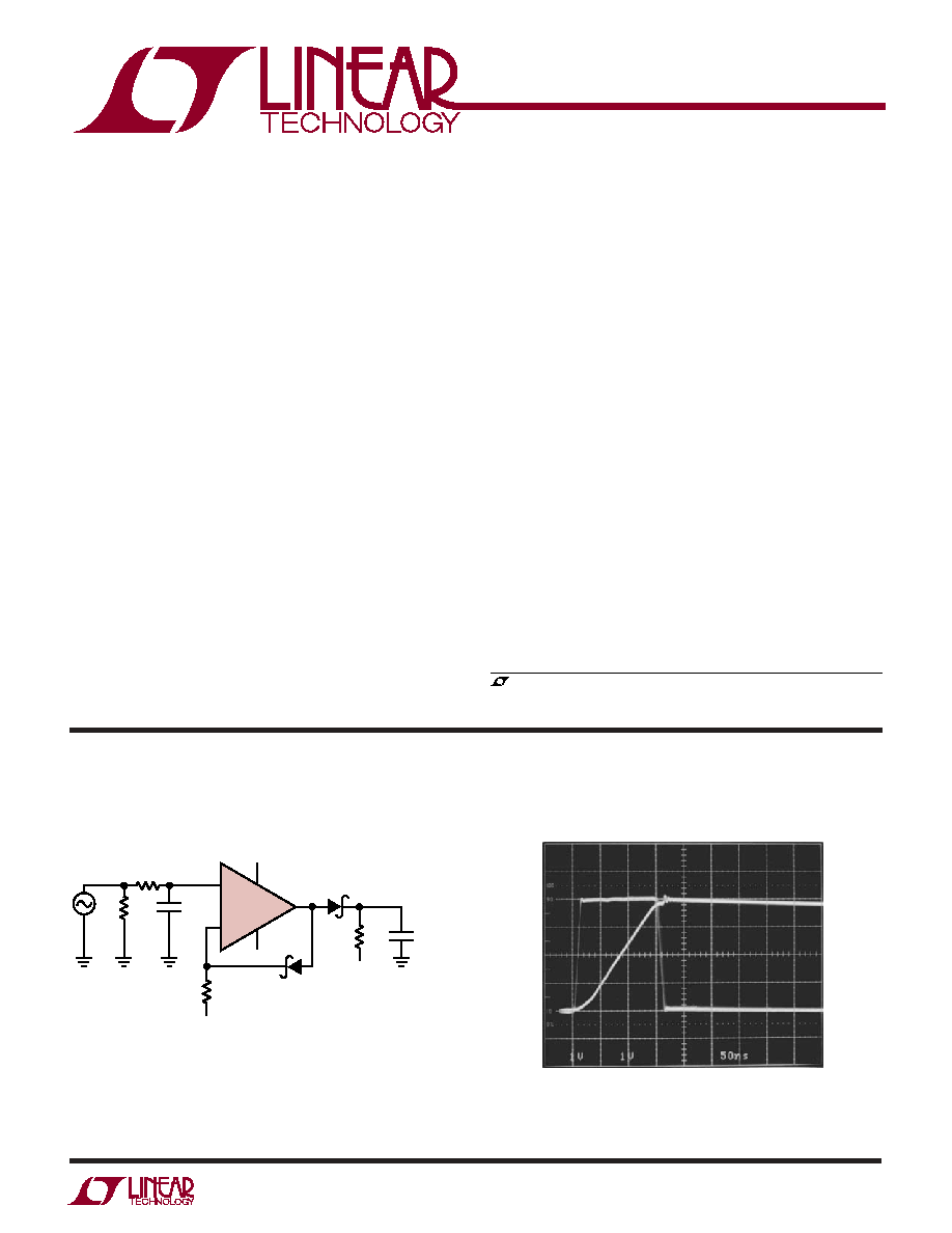
Fast Pulse Detector
Pulse Detector Response
+
LT1195
R
S
50
V
IN
D2
1N5712
D1
1N5712
R
L
10k
5V
5V
R
B
10k
5V
5V
C
L
1000pF
C
I
60pF
R
I
1k
1195 TA01
3
2
4
7
6
1195TAO2
OUTPUT
INPUT
, LTC and LT are registered trademarks of Linear Technology Corporation
2
LT1195
1195fa
LT1195M/C
SYMBOL
PARAMETER
CONDITIONS
MIN
TYP
MAX
UNITS
V
OS
Input Offset Voltage
J8, N8 Package
3.0
8.0
mV
S8 Package
3.0
10.0
mV
I
OS
Input Offset Current
0.2
1.0
µA
I
B
Input Bias Current
±0.5
±2.0
µA
e
n
Input Noise Voltage
f
O
= 10kHz
70
nVHz
i
n
Input Noise Current
f
O
= 10kHz
2
pAHz
R
IN
Input Resistance Differential Mode
230
k
Common Mode
20
M
C
IN
Input Capacitance
A
V
= 1
2.2
pF
Input Voltage Range
(Note 4)
2.5
3.5
V
CMRR
Common Mode Rejection Ratio
V
CM
= 2.5 to 3.5V
60
85
dB
PSRR
Power Supply Rejection Ratio
V
S
= ±2.375V to ±8V
60
85
dB
A
VOL
Large-Signal Voltage Gain
R
L
= 1k, V
OUT
= ±3V
2.0
7.5
V/mV
R
L
= 150, V
OUT
= ±3V
0.5
1.5
V/mV
V
S
= ±8V, R
L
= 1k, V
OUT
= ±5V
11.0
V/mV
V
OUT
Output Voltage Swing
V
S
= ±5V, R
L
= 1k
±3.8
±4.0
V
V
S
= ±8V, R
L
= 1k
±6.7
±7.0
V
SR
Slew Rate
A
V
= 1, R
L
= 1k (Note 5, 10)
110
165
V/µs
FPBW
Full Power Bandwidth
V
OUT
= 6V
P-P
(Note 6)
8.75
MHz
GBW
Gain-Bandwidth Product
50
MHz
t
r1
, t
f1
Rise Time, Fall Time
A
V
= 50, V
OUT
= ±1.5V, 20% to 80% (Note 10)
125
170
285
ns
t
r2
, t
f2
Rise Time, Fall Time
A
V
= 1, V
OUT
= ±125mV, 10% to 90%
3.4
ns
t
PD
Propagation Delay
A
V
= 1, V
OUT
= ±125mV, 50% to 50%
2.5
ns
Overshoot
A
V
= 1, V
OUT
= ±125mV
22
%
t
S
Settling Time
3V Step, 0.1% (Note 7)
220
ns
Diff A
V
Differential Gain
R
L
= 150, A
V
= 2 (Note 8)
1.25
%
Diff Ph
Differential Phase
R
L
= 150, A
V
= 2 (Note 8)
0.86
DEG
P-P
S8 PART MARKING
Total Supply Voltage (V
+
to V
) ............................... 18V
Differential Input Voltage ......................................... ±6V
Input Voltage ........................................................... ±V
S
Output Short-Circuit Duration (Note 2) ......... Continuous
Operating Temperature Range
LT1195M (OBSOLETE) ................... 55°C to 125°C
LT1195C ................................................ 0°C to 70°C
Junction Temperature (Note 3)
Plastic Package (CN8, CS8) ............................ 150°C
Ceramic Package (CJ8, MJ8) (OBSOLETE) ..... 175°C
Storage Temperature Range ................. 65°C to 150°C
Lead Temperature (Soldering, 10 sec).................. 300°C
ORDER PART
NUMBER
1
2
3
4
8
7
6
5
TOP VIEW
BAL
IN
+IN
V
BAL
V
+
OUT
S/D
S8 PACKAGE
8-LEAD PLASTIC SO
J8 PACKAGE
8-LEAD CERDIP
N8 PACKAGE
8-LEAD PDIP
T
JMAX
= 150°C,
JA
= 100°C/ W (J8)
V
S
= ±5V, C
L
10pF, Pin 5 open circuit, unless otherwise noted.
LT1195CN8
LT1195CS8
T
JMAX
= 150°C,
JA
= 100°C/ W (N8)
T
JMAX
= 150°C,
JA
= 150°C/ W (S8)
Consult LTC Marketing for parts specified with wider operating temperature ranges.
OBSOLETE PACKAGE
Consider the N8 or S8 Package for Alternate Source
LT1195MJ8
LT1195CJ8
1195
ORDER PART
NUMBER
(Note 1)
T
A
= 25°C
ABSOLUTE AXI U RATI GS
W
W
W
U
PACKAGE/ORDER I FOR ATIO
U
U
W
5V ELECTRICAL CHARACTERISTICS
+
3
LT1195
1195fa
LT1195M/C
SYMBOL
PARAMETER
CONDITIONS
MIN
TYP
MAX
UNITS
V
OS
Input Offset Voltage
J8, N8 Package
3.0
9.0
mV
S8 Package
3.0
11.0
mV
I
OS
Input Offset Current
0.2
1.0
µA
I
B
Input Bias Current
±0.5
±2.0
µA
Input Voltage Range
(Note 4)
2.0
3.5
V
CMRR
Common Mode Rejection Ratio
V
CM
= 2V to 3.5V
60
85
dB
A
VOL
Large-Signal Voltage Gain
R
L
= 150 to Ground, V
OUT
= 1V to 3V
0.5
3.0
V/mV
V
OUT
Output Voltage Swing
R
L
= 150 to Ground V
OUT
High
3.5
3.8
V
V
OUT
Low
0.25
0.4
V
SR
Slew Rate
A
V
= 1, V
OUT
= 1V to 3V
140
V/µs
GBW
Gain-Bandwidth Product
45
MHz
I
S
Supply Current
11
15
mA
Shutdown Supply Current
Pin 5 at V
0.8
1.5
mA
I
S/D
Shutdown Pin Current
Pin 5 at V
5
25
µA
LT1195M/C
SYMBOL
PARAMETER
CONDITIONS
MIN
TYP
MAX
UNITS
I
S
Supply Current
12
16
mA
Shutdown Supply Current
Pin 5 at V
0.8
1.5
mA
I
S/D
Shutdown Pin Current
Pin 5 at V
5
25
µA
t
ON
Turn-On Time
Pin 5 from V
to Ground, R
L
= 1k
160
ns
t
OFF
Turn-Off Time
Pin 5 from Ground to V
,
R
L
= 1k
700
ns
V
S
= ±5V, C
L
10pF, Pin 5 open circuit, unless otherwise noted.
V
S
+
= 5V, V
S
, = OV, V
CM
= 2.5V, C
L
10pF, Pin 5 open circuit, unless otherwise noted.
LT1195M
SYMBOL
PARAMETER
CONDITIONS
MIN
TYP
MAX
UNITS
V
OS
Input Offset Voltage
3.0
15.0
mV
V
OS
/T
Input V
OS
Drift
17
µV/°C
I
OS
Input Offset Current
0.2
2.0
µA
I
B
Input Bias Current
±0.5
±2.5
µA
CMRR
Common Mode Rejection Ratio
V
CM
= 2.5V to 3.5V
55
85
dB
PSRR
Power Supply Rejection Ratio
V
S
= ±2.375V to ±8V
55
80
dB
A
VOL
Large-Signal Voltage Gain
R
L
= 1k, V
OUT
= ±3V
1.50
5.0
V/mV
R
L
= 150, V
OUT
= ±3V
0.25
0.8
V/mV
V
OUT
Output Voltage Swing
R
L
= 1k
±3.7
±3.9
V
I
S
Supply Current
12
18
mA
Shutdown Supply Current
Pin 5 at V
, (Note 9)
0.8
2.5
mA
I
S/D
Shutdown Pin Current
Pin 5 at V
5
25
µA
V
S
= ±5V, Pin 5 open circuit, unless otherwise noted.
55°C T
A
125°C, (Note 11)
T
A
= 25°C
T
A
= 25°C
5V ELECTRICAL CHARACTERISTICS
+
5V ELECTRICAL CHARACTERISTICS
+
5V ELECTRICAL CHARACTERISTICS
4
LT1195
1195fa
LT1195C
SYMBOL
PARAMETER
CONDITIONS
MIN
TYP
MAX
UNITS
V
OS
Input Offset Voltage
J8, N8 Package
1.0
10.0
mV
S8 Package
1.0
15.0
mV
V
OS
/T
Input V
OS
Drift
15
µV/°C
I
OS
Input Offset Current
0.2
1.7
µA
I
B
Input Bias Current
±0.5
±2.5
µA
Input Voltage Range
(Note 4)
2.0
3.5
V
CMRR
Common Mode Rejection Ratio
V
CM
= 2V to 3.5V
60
85
dB
V
OUT
Output Voltage Swing
R
L
= 150 to Ground V
OUT
High
3.5
3.75
V
V
OUT
Low
0.15
0.4
V
I
S
Supply Current
12
16
mA
Shutdown Supply Current
Pin 5 at V
(Note 9)
0.9
2.0
mA
I
S/D
Shutdown Pin Current
Pin 5 at V
5
25
µA
LT1195C
SYMBOL
PARAMETER
CONDITIONS
MIN
TYP
MAX
UNITS
V
OS
Input Offset Voltage
J8, N8 Package
3.0
10.0
mV
S8 Package
3.0
15.0
mV
V
OS
/T
Input V
OS
Drift
12
µV/°C
I
OS
Input Offset Current
0.2
1.7
µA
I
B
Input Bias Current
±0.5
±2.5
µA
CMRR
Common Mode Rejection Ratio
V
CM
= 2.5V to 3.5V
60
85
dB
PSRR
Power Supply Rejection Ratio
V
S
= ±2.375V to ±5V
60
90
dB
A
VOL
Large-Signal Voltage Gain
R
L
= 1k, V
OUT
= ±3V
2.0
7.5
V/mV
R
L
= 150, V
OUT
= ±3V
0.3
1.5
V/mV
V
OUT
Output Voltage Swing
R
L
= 1k
±3.7
±3.9
V
I
S
Supply Current
12
17
mA
Shutdown Supply Current
Pin 5 at V
(Note 9)
0.9
2.0
mA
I
S/D
Shutdown Pin Current
Pin 5 at V
5
25
µA
0°C T
A
70°C
V
S
= ±5V, Pin 5 open circuit, unless otherwise noted.
0°C T
A
70°C
V
S
+
= 5V, V
S
= OV, Pin 5 open circuit, unless otherwise noted.
Note 1: Absolute Maximum Ratings are those values beyond which the life
of a device may be impaired.
Note 2: A heat sink may be required to keep the junction temperature
below absolute maximum when the output is shorted continuously.
Note 3: T
J
is calculated from the ambient temperature T
A
and power
dissipation P
D
according to the following formats:
LT1195MJ8/LT1195CJ8:
T
J
= T
A
+ (P
D
· 100°C/ W)
LT1195N:
T
J
= T
A
+ (P
D
· 100°C/ W)
LT1195CS:
T
J
= T
A
+ (P
D
· 150°C/ W)
Note 4: Exceeding the input common mode range may cause the output
to invert.
Note 5: Slew rate is measured between ±1V on the output, with ±3V input
step.
Note 6: Full power bandwidth is calculated from the slew rate
measurement: FPBW = SR/2V
P.
Note 7: Settling time measurement techniques are shown in "Take the
Guesswork Out of Settling Time Measurements," EDN, September 19, 1985.
Note 8: NTSC (3.58MHz). For R
L
= 1k, Diff A
V
= 0.3%, Diff Ph = 0.35°.
Note 9: See Applications Information section for shutdown at elevated
temperatures. Do not operate the shutdown above T
J
> 125°C.
Note 10: AC parameters are 100% tested on the ceramic and plastic DIP
packaged parts (J8 and N8 suffix) and are sample tested on every lot of
the SO packaged parts (S8 suffix).
Note 11: Do not operate at A
V
< 2 for T
A
< 0°C.
5V ELECTRICAL CHARACTERISTICS
+
5V ELECTRICAL CHARACTERISTICS
5
LT1195
1195fa
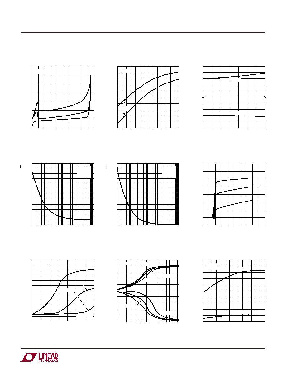
TYPICAL PERFOR A CE CHARACTERISTICS
U
W
TEMPERATURE (°C)
50
COMMON MODE RANGE (V)
V
+
0.5
1.0
1.5
2.0
2.0
1.5
1.0
0.5
V
0
25
75
125
1195 G03
25
50
100
V
+
= 1.8V TO 9V
V
+
= 1.8V TO 9V
Common Mode Voltage vs
Temperature
Equivalent Input Noise Voltage
vs Frequency
Equivalent Input Noise Current
vs Frequency
Output Voltage Swing vs
Load Resistance
COMMON MODE VOLTAGE (V)
5
INPUT BIAS CURRENT ( A)
3.0
2.5
2.0
1.5
1.0
0.5
0
0.5
2
0
2
4
1195 G01
µ
4
1
1
3
3
5
V
S
= ±5V
55°C
25°C
125°C
TEMPERATURE (°C)
50
INPUT BIAS CURRENT (nA)
100
0
100
200
300
400
0
25
75
125
1195 G02
25
50
100
+I
B
I
B
I
OS
V
S
= ±5V
Input Bias Current vs
Temperature
Input Bias Current vs
Common Mode Voltage
FREQUENCY (Hz)
EQUIVALENT INPUT NOISE VOLTAGE (nV/
Hz)
600
500
400
300
200
100
0
10
1k
10k
100k
1195 G04
100
V
S
= ±5V
T
A
= 25°C
R
S
= 0
FREQUENCY (Hz)
EQUIVALENT INPUT NOISE CURRENT (pA/
Hz)
14
12
10
8
6
4
2
10
1k
10k
100k
1195 G05
100
V
S
= ±5V
T
A
= 25°C
R
S
= 100k
±SUPPLY VOLTAGE (V)
0
SUPPLY CURRENT (mA)
16
14
12
10
8
2
4
6
10
1195 G06
8
55°C
125°C
25°C
Supply Current vs Supply Voltage
Shutdown Supply Current
vs Temperature
LOAD RESISTANCE ()
10
OUTPUT VOLTAGE SWING (V)
5
3
1
1
3
5
100
1k
1195 G08
T
A
= 55°C
T
A
= 125°C
T
A
= 25°C
V
S
= ±5V
T
A
= 125°C
T
A
= 25°C
T
A
= 55°C
TEMPERATURE (°C)
50
OPEN-LOOP GAIN (V/V)
10k
8k
6k
4k
2k
0
0
25
75
125
1195 G09
25
50
100
R
L
= 1k
V
S
= ±5V
V
O
= ±3V
R
L
= 150
Open-Loop Gain vs Temperature
TEMPERATURE (°C)
50
SHUTDOWN SUPPLY CURRENT (mA)
6
5
4
3
2
1
0
0
25
75
125
1195 G07
25
50
100
V
S
= ±5V
V
S/D
= V
EE
+ 0.6V
V
S/D
= V
EE
+ 0.2V
V
S/D
= V
EE
+ 0.4V
V
S/D
= V
EE