 | –≠–ª–µ–∫—Ç—Ä–æ–Ω–Ω—ã–π –∫–æ–º–ø–æ–Ω–µ–Ω—Ç: LT1203 | –°–∫–∞—á–∞—Ç—å:  PDF PDF  ZIP ZIP |
1
LT1203/LT1205
150MHz Video Multiplexers
s
≠ 3dB Bandwidth: 150MHz
s
0.1dB Gain Flatness: 30MHz
s
Channel-to-Channel Switching Time: 25ns
s
Turn-On/Turn-Off Time: 25ns
s
High Slew Rate: 300V/
µ
s
s
Disabled Output Impedance: 10M
s
50mV Switching Transient
s
Channel Separation at 10MHz: > 90dB
s
Differential Gain: 0.02%
s
Differential Phase: 0.02
∞
s
Wide Supply Range:
±
5V to
±
15V
s
Output Short-Circuit Protected
s
Push-Pull Output
S
FEATURE
D
U
ESCRIPTIO
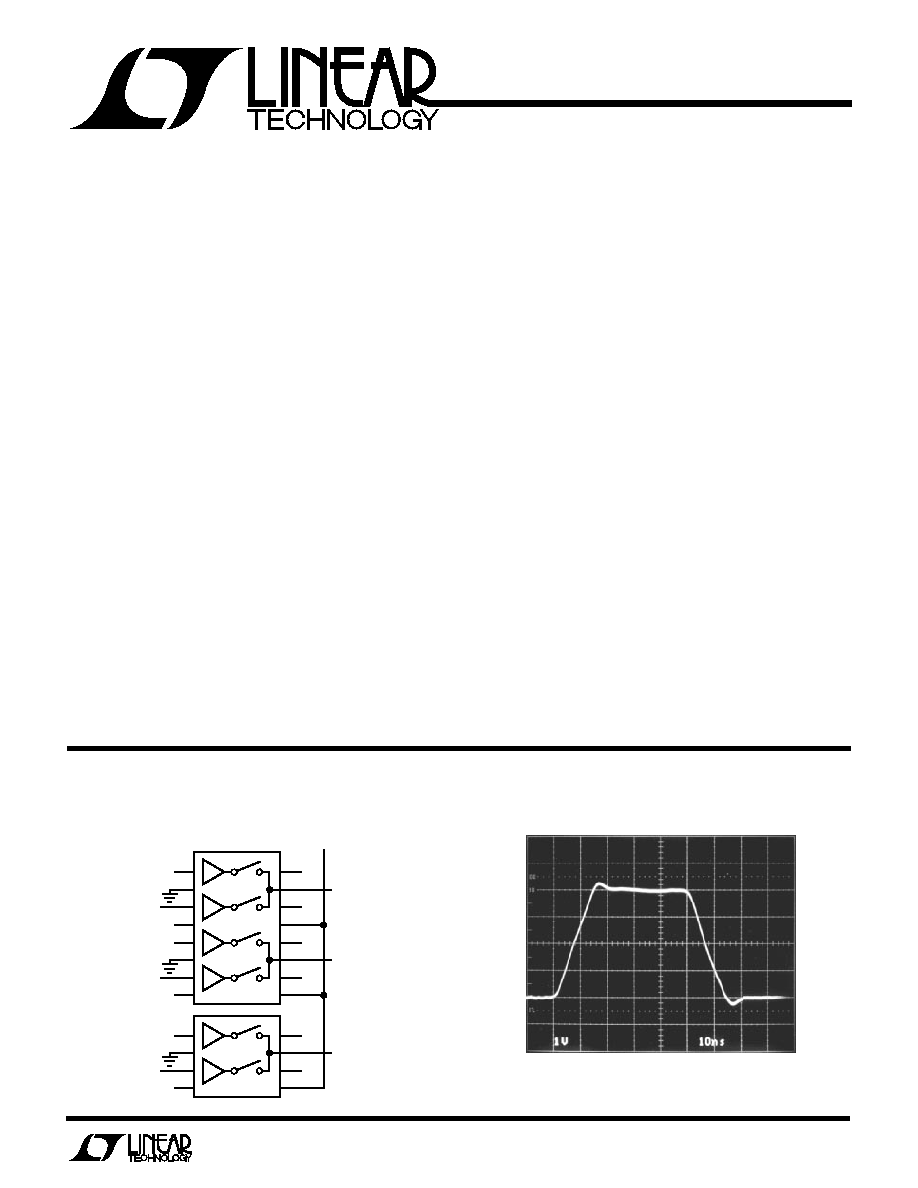
The LT1203 is a wideband 2-input video multiplexer
designed for pixel switching and broadcast quality rout-
ing. The LT1205 is a dual version that is configured as a
4-input, 2-output multiplexer.
These multiplexers act as SPDT video switches with 10ns
transition times at toggle rates up to 30MHz. The ≠ 3dB
bandwidth is 150MHz and 0.1dB gain flatness is 30MHz.
Many parts can be tied together at their outputs by using
the enable feature which reduces the power dissipation
and raises the output impedance to 10M
. Output capaci-
tance when disabled is only 3pF and the LT1203 peaks less
than 3dB into a 50pF load. Channel crosstalk and disable
isolation are greater than 90dB up to 10MHz. An on-chip
buffer interfaces to fast TTL or CMOS logic. Switching
transients are only 50mV with a 25ns duration. The
LT1203 and LT1205 outputs are protected against shorts
to ground.
The LT1203/LT1205 are manufactured using Linear
Technology's proprietary complementary bipolar process.
The LT1203 is available in both the 8-lead PDIP and SO
package while the LT1205 is available in the 16-lead
narrow body SO package.
U
A
O
PPLICATI
TYPICAL
+1
+1
+1
+1
LT1205
LOGIC
V
+
LOGIC
V
OUT
RED
V
OUT
GREEN
V
OUT
BLUE
LT1203 ∑ TA01
EN
RED 1
CHANNEL SELECT
RED 2
GREEN 1
GREEN 2
BLUE 1
BLUE 2
V
≠
V
≠
V
≠
EN
V
+
+1
+1
LT1203
LOGIC
EN
V
+
High Speed RGB MUX
Large-Signal Response
U
S
A
O
PPLICATI
s
Broadcast Quality Video Multiplexing
s
Picture-in-Picture Switching
s
HDTV
s
Computer Graphics
s
Title Generation
s
Video Crosspoint Matrices
s
Video Routers

2
LT1203/LT1205
A
U
G
W
A
W
U
W
A
R
BSOLUTE
XI
TI
S
Supply Voltage ......................................................
±
18V
Signal Input Current (Note 1) ............................
±
20mA
Logic Input Current (Note 2)..............................
±
50mA
Output Short-Circuit Duration (Note 3) ........ Continuous
Specified Temperature Range (Note 4) ....... 0
∞
C to 70
∞
C
Operating Temperature Range ............... ≠ 40
∞
C to 85
∞
C
Storage Temperature Range ................ ≠ 65
∞
C to 150
∞
C
Junction Temperature (Note 5) ............................ 150
∞
C
Lead Temperature (Soldering, 10 sec) ................. 300
∞
C
ORDER PART
NUMBER
LT1203CN8*
LT1203CS8*
S8 PART MARKING
1203
*See Note 4
Consult factory for Industrial and Military grade parts.
ORDER PART
NUMBER
LT1205CS*
T
JMAX
= 150
∞
C,
JA
= 100
∞
C/W
TOP VIEW
S PACKAGE
16-LEAD PLASTIC SOIC
1
2
3
4
5
6
7
8
16
15
14
13
12
11
10
9
V
INO
GND
V
IN1
V
≠
V
IN2
GND
V
IN3
V
≠
V
+
V
OUT1
EN1
LOGIC 1
V
+
V
OUT2
EN2
LOGIC 2
1
2
3
4
8
7
6
5
TOP VIEW
V
IN0
GND
V
IN1
V
≠
V
+
V
OUT
EN
LOGIC
N8 PACKAGE
8-LEAD PLASTIC DIP
S8 PACKAGE
8-LEAD PLASTIC SOIC
T
JMAX
= 150
∞
C,
JA
= 100
∞
C/W (N)
T
JMAX
= 150
∞
C,
JA
= 150
∞
C/W (S)
W
U
U
PACKAGE/ORDER I FOR ATIO
SYMBOL
PARAMETER
CONDITIONS
MIN
TYP
MAX
UNITS
V
OS
Output Offset Voltage
Any Input Selected
q
10
30
mV
Output Offset Matching
Between Outputs
q
0.3
5
mV
V
OS
/
T
Output Offset Drift
q
40
µ
V/
∞
C
I
IN
Input Current
q
0.6
5
µ
A
R
IN
Input Resistance
V
S
=
±
5V, V
IN
=
±
2V
q
1
5
M
V
S
=
±
15V, V
IN
=
±
2V
q
2
5
M
C
IN
Input Capacitance
Input Selected
2.6
pF
Input Deselected
2.6
pF
C
OUT
Disabled Output Capacitance
EN Pin Voltage
0.8V
2.8
pF
V
IN
Input Voltage (Note 1)
V
S
=
±
5V
q
±
2
±
2.8
V
V
S
=
±
15V
q
±
2
±
3.0
V
PSRR
Power Supply Rejection Ratio
V
S
=
±
4.5 to
±
15V
q
60
70
dB
Gain Error
V
S
=
±
15V, V
IN
=
±
2V, R
L
= 1k
q
2
4
%
V
S
=
±
15V, V
IN
=
±
2V, R
L
= 400
q
6
10
%
V
S
=
±
5V, V
IN
=
±
2V, R
L
= 1k
q
3
6
%
ELECTRICAL C
C
HARA TERISTICS
0
∞
C
T
A
70
∞
C,
±
5V
V
S
±
15V, R
L
= 1k, pulse tested, EN pin open or high, unless otherwise noted.

3
LT1203/LT1205
SYMBOL
PARAMETER
CONDITIONS
MIN
TYP
MAX
UNITS
SR
Slew Rate (Note 6)
180
300
V/
µ
s
FPBW
Full Power Bandwidth (Note 7)
V
OUT
= 2V
P-P
28.6
47.7
MHz
t
SEL
Channel-to-Channel Select Time (Note 8) R
L
= 10k
25
35
ns
Enable Time (Note 9)
R
L
= 1k
25
35
ns
Disable Time (Note 9)
R
L
= 1k
20
35
ns
t
r
, t
f
Small-Signal Rise and Fall Time
V
OUT
= 250mV
P-P
, 10% to 90%
2.6
ns
Propagation Delay
V
OUT
= 250mV
P-P
2.9
ns
Overshoot
V
OUT
= 250mV
P-P
5
%
Crosstalk (Note 10)
R
S
= 10
90
dB
Chip Disabled Crosstalk (Note 10)
R
L
= 10
, EN Pin Voltage
0.8V
110
dB
Channel Select Output Transient
All V
IN
= 0V
50
mV
P-P
t
S
Settling Time
1%, V
OUT
= 1V
30
ns
Differential Gain (Note 11)
V
S
=
±
15V, R
L
= 10k
0.02
%
Differential Phase (Note 11)
V
S
=
±
15V, R
L
= 10k
0.02
DEG
Insertion Loss
R
L
= 100k, C
L
= 30pF, V
OUT
= 500mV
P-P
, f = 1MHz
0.02
dB
ELECTRICAL C
C
HARA TERISTICS
0
∞
C
T
A
70
∞
C,
±
5V
V
S
±
15V, R
L
= 1k, pulse tested, EN pin open or high, unless otherwise noted.
SYMBOL
PARAMETER
CONDITIONS
MIN
TYP
MAX
UNITS
V
OUT
Output Voltage
V
S
=
±
15V, V
IN
=
±
2V, R
L
= 400
q
±
1.8
±
1.90
V
V
S
=
±
5V, V
IN
=
±
2V, R
L
= 1k
q
±
1.8
±
1.94
V
Overload Swing (Note 1)
V
S
=
±
15V, V
IN
=
±
5V
q
±
0.9
±
1.5
V
V
S
=
±
5V, V
IN
=
±
5V
q
±
0.9
±
1.5
V
I
OUT
Output Current
V
S
=
±
15V, V
IN
=
±
2V, R
L
= 400
q
±
4.5
±
4.75
mA
V
S
=
±
5V, V
IN
=
±
2V, R
L
= 1k
q
±
1.8
±
2.00
mA
R
OUT
Enabled Output Resistance
EN Pin Voltage = 2V, V
OUT
=
±
2V, V
S
=
±
15V
q
20
42
Disabled Output Resistance
EN Pin Voltage = 0.5V, V
OUT
=
±
2V, V
S
=
±
15V
q
1
10
M
I
S
Supply Current (LT1203)
EN Pin Voltage = 2V
q
10.0
14
mA
EN Pin Voltage = 0.5V
q
5.8
8
mA
Supply Current (LT1205)
EN Pin Voltage = 2V
q
20.0
28
mA
EN Pin Voltage = 0.5V
q
11.6
16
mA
V
IL
Logic Low
Logic Pin
q
0.8
V
V
IH
Logic High
Logic Pin
q
2
V
Enable Low
EN Pin
q
0.5
V
Enable High
EN Pin
q
2
V
I
IL
Digital Input Current Low
LT1203 Pin 5, LT1205 Pins 9, 13 = 0V
q
1.5
6.5
µ
A
I
IH
Digital Input Current High
LT1203 Pin 5, LT1205 Pins 9, 13 = 5V
q
10
200
nA
I
EN
Enable Pin Current
LT1203 Pin 6, LT1205 Pins 10, 14
q
20
80
µ
A
C
C
HARA TERISTICS
AC
T
A
= 25
∞
C, V
S
=
±
15V, R
L
= 1k, EN pin open or high, unless otherwise noted.
The
q
denotes specifications which apply over the specified
temperature range.
Note 1: The analog inputs (pins 1, 3 for the LT1203, pins 1, 3, 5, 7 for the
LT1205) are protected against ESD and overvoltage with internal SCRs.
For inputs
±
2.8V the SCR will not fire. Voltages above 2.8V will fire the
SCR and the DC current should be limited to 20mA. To turn off the SCR
the pin voltage must be reduced to less than 1V or the current reduced to
less than 600
µ
A.

4
LT1203/LT1205
Note 2: The digital inputs (pins 5, 6 for the LT1203, pins 9, 10, 13, 14 for
the LT1205) are protected against ESD and overvoltage with internal
SCRs. For inputs
±
6V the SCR will not fire. Voltages above 6V will fire
the SCR and the DC current should be limited to 50mA. To turn off the
SCR the pin voltage must be reduced to less than 2V or the current
reduced to less than 10mA.
Note 3: A heat sink may be required depending on the power supply
voltage.
Note 4: Commercial grade parts are designed to operate over the
temperature range of ≠ 40
∞
C to 85
∞
C but are neither tested nor guaranteed
beyond 0
∞
C to 70
∞
C. Industrial grade parts specified and tested over
≠ 40
∞
C to 85
∞
C are available on special request, consult factory.
Note 5: T
J
is calculated from the ambient temperature T
A
and the power
dissipation P
D
according to the following formulas:
LT1203CN8: T
J
= T
A
+ (P
D
◊
100
∞
C/W)
LT1203CS8: T
J
= T
A
+ (P
D
◊
150
∞
C/W)
LT1205CS: T
J
= T
A
+ (P
D
◊
100
∞
C/W)
Note 6: Slew rate is measured at
±
2.0V on a
±
2.5V output signal while
operating on
±
15V supplies, R
L
= 1k.
Note 7: Full power bandwidth is calculated from the slew rate
measurement:
FPBW = SR/2
V
PEAK
Note 8: For the LT1203, apply 1VDC to pin 1 and measure the time for the
appearance of 0.5V at pin 7 when pin 5 goes from 5V to 0V. Apply 1VDC
to pin 1 and measure the time for disappearance of 0.5V at pin 7 when
pin 5 goes from 0V to 5V. Apply 1VDC to pin 3 and measure the time for
the appearance of 0.5V at pin 7 when pin 5 goes from 0V to 5V. Apply
1VDC to pin 3 and measure the time for disappearance of 0.5V at pin 7
when pin 5 goes from 5V to 0V. For the LT1205 the same test is
performed on both MUXs.
Note 9: For the LT1203, apply 1VDC to pin 1 and measure the time for the
appearance of 0.5V at pin 7 when pin 6 goes from 0V to 5V. Pin 5 voltage
= 0V. Apply 1VDC to pin 1 and measure the time for disappearance of 0.2V
at pin 7 when pin 6 goes from 5V to 0V. Pin 5 voltage = 0V. Apply 1VDC
to pin 3 and measure the time for the appearance of 0.5V at pin 7 when
pin 6 goes from 0V to 5V. Pin 5 voltage = 5V. Apply 1VDC to pin 3 and
measure the time for disappearance of 0.2V at pin 7 when pin 5 goes from
5V to 0V. Pin 5 voltage = 5V. For the LT1205 the same test is performed
on both MUXs.
Note 10: V
IN
= 0dBm (0.223V
RMS
) at 10MHz on one input with the other
input selected and R
S
= 10
. For disable crosstalk all inputs are driven
simultaneously. In disable the output impedance is very high and signal
couples across the package; the load impedance determines the crosstalk.
Note 11: Differential gain and phase are measured using a Tektronix
TSG120 YC/NTSC signal generator and a Tektronix 1780R video
measurement set. The resolution of this equipment is 0.1% and 0.1
∞
.
Ten identical MUXs were cascaded giving an effective resolution of
0.01% and 0.01
∞
.
TYPICAL PERFOR A CE CHARACTERISTICS
W U
LOGIC
EN
V
OUT
0
1
V
IN0
1
1
V
IN1
0
0*
HIGH Z
OUT
1
0
HIGH Z
OUT
*Must be
0.5V
TRUTH TABLE
FREQUENCY (MHz)
1
≠1
GAIN (dB)
PHASE (DEG)
0
1
2
3
10
100
1000
LT1203/05 ∑ TPC02
≠2
≠3
≠4
≠5
4
5
≠120
≠100
≠80
≠60
≠40
≠140
≠160
≠180
≠200
≠20
0
V
S
= ±15V
T
A
= 25∞C
R
L
=
FREQUENCY (MHz)
1
≠1
GAIN (dB)
PHASE (DEG)
0
1
2
3
10
100
1000
LT1203/05 ∑ TPC01
≠2
≠3
≠4
≠5
4
5
≠120
≠100
≠80
≠60
≠40
≠140
≠160
≠180
≠200
≠20
0
V
S
= ±5V
T
A
= 25∞C
R
L
=
±
5V Frequency Response
±
15V Frequency Response

5
LT1203/LT1205
TYPICAL PERFOR A CE CHARACTERISTICS
W U
Frequency Response
with Capacitive Loads
Disable Rejection
vs Frequency
Crosstalk Rejection
vs Frequency
Output Impedance (Enabled)
vs Frequency
Crosstalk Rejection
vs Frequency
SUPPLY VOLTAGE (±V)
0
FREQUENCY (MHz)
160
180
18
LT1203/05 ∑ TPC03
140
120
2
6
8
10
12
14
16
4
200
T
A
= 25∞C
R
L
= 10k
PEAKING
0.5dB
FREQUENCY (MHz)
1
≠5
GAIN (dB)
≠3
≠1
1
3
10
100
LT1203/05 ∑ TPC04
≠4
≠2
0
2
4
5
V
S
= ±15V
T
A
= 25∞C
R
L
=
C
L
= 100pF
C
L
= 50pF
C
L
= 20pF
C
L
= 10pF
FREQUENCY (MHz)
1
≠110
CROSSTALK REJECTION (dB)
≠100
≠90
≠80
≠70
≠30
10
100
LT1203/05 ∑ TPC05
≠ 60
≠50
≠ 40
V
S
= ±15V
T
A
= 25∞C
R
L
=
R
S
= 0
R
S
= 10
R
S
= 37.5
R
S
= 75
FREQUENCY (MHz)
1
≠110
CROSSTALK REJECTION (dB)
≠100
≠ 90
≠80
≠70
≠30
10
100
LT1203/05 ∑ TPC06
≠ 60
≠50
≠ 40
T
A
= 25∞C
R
S
= 0
R
L
=
V
S
= ±5V
V
S
= ±15V
FREQUENCY (MHz)
1
≠70
≠80
≠90
≠100
≠110
≠120
DISABLE REJECTION (dB)
≠ 60
≠50
≠ 40
≠30
10
100
LT1203/05 ∑ TPC07
≠20
V
S
= ±15V
T
A
= 25∞C
R
L
=
R
L
= 1k
R
L
= 100
R
L
= 10
FREQUENCY (MHz)
0
30
20
10
70
60
50
40
LT1203/05 ∑ TPC08
POWER SUPPLY REJECTION RATIO (dB)
1
100
10
V
S
= ±15V
T
A
= 25∞C
R
L
=
R
S
= 0
≠PSRR
+PSRR
Supply Current
vs Supply Voltage (Enabled)
Supply Current
vs Supply Voltage (Disabled)
FREQUENCY (Hz)
20
OUTPUT IMPEDANCE (
)
40
30
60
80
100
10k
1M
100M
10M
LT1203/05 ∑ TPC09
10
100k
V
S
= ±15V
T
A
= 25∞C
SUPPLY VOLTAGE (±V)
0
7.6
SUPPLY CURRENT (mA)
8.4
9.6
4
8
10
18
LT1203/05 ∑ TPC10
8.0
9.2
8.8
2
6
12
14
16
LT1203
R
L
=
125∞
25∞
≠55∞
SUPPLY VOLTAGE (±V)
0
4.4
SUPPLY CURRENT (mA)
4.8
4
8
10
18
LT1203/05 ∑ TPC11
4.6
5.2
5.0
2
6
12
14
16
125∞
25∞
LT1203
R
L
=
≠55∞
≠ 3dB Bandwidth
vs Supply Voltage
Power Supply Rejection Ratio
vs Frequency