 | –≠–ª–µ–∫—Ç—Ä–æ–Ω–Ω—ã–π –∫–æ–º–ø–æ–Ω–µ–Ω—Ç: LT1355 | –°–∫–∞—á–∞—Ç—å:  PDF PDF  ZIP ZIP |
1
LT1355/LT1356
Dual and Quad
12MHz, 400V/
µ
s Op Amps
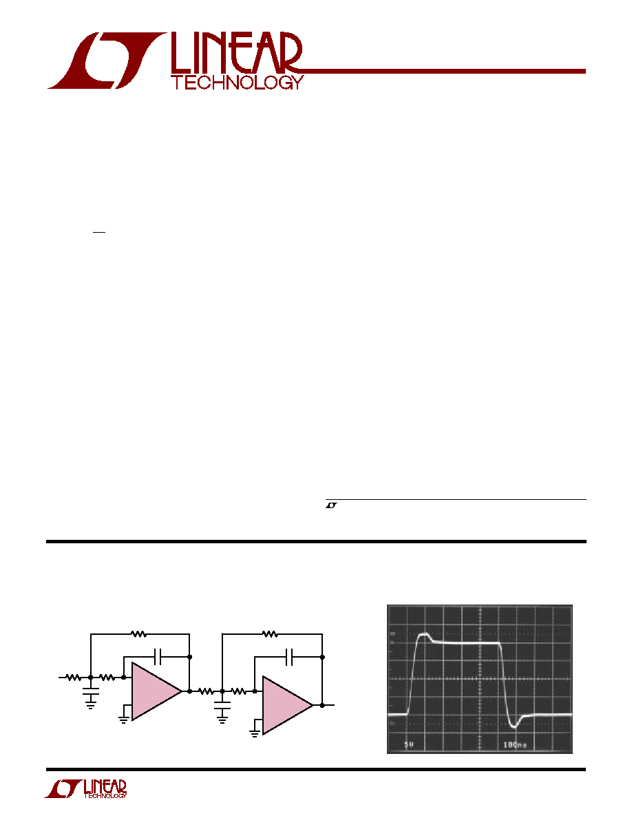
1355/1356 TA01
V
IN
5.23k
10.2k
47pF
6.81k
100pF
1000pF
V
OUT
≠
+
≠
+
5.23k
11.3k
6.81k
330pF
1/2
LT1355
1/2
LT1355
100kHz, 4th Order Butterworth Filter
1355/1356 TA02
A
V
= ≠1 Large-Signal Response
s
12MHz Gain Bandwidth
s
400V/
µ
s Slew Rate
s
1.25mA Maximum Supply Current per Amplifier
s
Unity-Gain Stable
s
C-Load
TM
Op Amp Drives All Capacitive Loads
s
10nV/
Hz Input Noise Voltage
s
800
µ
V Maximum Input Offset Voltage
s
300nA Maximum Input Bias Current
s
70nA Maximum Input Offset Current
s
12V/mV Minimum DC Gain, R
L
=1k
s
230ns Settling Time to 0.1%, 10V Step
s
280ns Settling Time to 0.01%, 10V Step
s
±
12.5V Minimum Output Swing into 500
s
±
3V Minimum Output Swing into 150
s
Specified at
±
2.5V,
±
5V, and
±
15V
The LT1355/LT1356 are dual and quad low power high
speed operational amplifiers with outstanding AC and DC
performance. The amplifiers feature much lower supply
current and higher slew rate than devices with comparable
bandwidth. The circuit topology is a voltage feedback
amplifier with matched high impedance inputs and the
slewing performance of a current feedback amplifier. The
high slew rate and single stage design provide excellent
settling characteristics which make the circuit an ideal
choice for data acquisition systems. Each output drives a
500
load to
±
12.5V with
±
15V supplies and a 150
load
to
±
3V on
±
5V supplies. The amplifiers are stable with any
capacitive load making them useful in buffer applications.
The LT1355/LT1356 are members of a family of fast, high
performance amplifiers using this unique topology and
employing Linear Technology Corporation's advanced
bipolar complementary processing. For a single amplifier
version of the LT1355/LT1356 see the LT1354 data sheet.
For higher bandwidth devices with higher supply currents
see the LT1357 through LT1365 data sheets. Bandwidths
of 25MHz, 50MHz, and 70MHz are available with 2mA,
4mA, and 6mA of supply current per amplifier. Singles,
duals, and quads of each amplifier are available.
s
Wideband Amplifiers
s
Buffers
s
Active Filters
s
Data Acquisition Systems
s
Photodiode Amplifiers
C-Load is a trademark of Linear Technology Corporation.
APPLICATIO S
U
FEATURES
TYPICAL APPLICATIO
U
DESCRIPTIO
U
, LTC and LT are registered trademarks of Linear Technology Corporation.
2
LT1355/LT1356
SYMBOL
PARAMETER
CONDITIONS
V
SUPPLY
MIN
TYP
MAX
UNITS
V
OS
Input Offset Voltage
±
15V
0.3
0.8
mV
±
5V
0.3
0.8
mV
±
2.5V
0.4
1.0
mV
I
OS
Input Offset Current
±
2.5V to
±
15V
20
70
nA
I
B
Input Bias Current
±
2.5V to
±
15V
80
300
nA
e
n
Input Noise Voltage
f = 10kHz
±
2.5V to
±
15V
10
nV/
Hz
i
n
Input Noise Current
f = 10kHz
±
2.5V to
±
15V
0.6
pA/
Hz
R
IN
Input Resistance
V
CM
=
±
12V
±
15V
70
160
M
Input Resistance
Differential
±
15V
11
M
C
IN
Input Capacitance
±
15V
3
pF
Total Supply Voltage (V
+
to V
≠
) ............................... 36V
Differential Input Voltage
(Transient Only) (Note 2)...................................
±
10V
Input Voltage ............................................................
±
V
S
Output Short-Circuit Duration (Note 3) ............ Indefinite
ABSOLUTE
M
AXI
M
U
M
RATINGS
W
W
W
U
Operating Temperature Range (Note 7) .. ≠ 40
∞
C to 85
∞
C
Specified Temperature Range (Note 8) ... ≠ 40
∞
C to 85
∞
C
Maximum Junction Temperature (See Below)
Plastic Package ................................................ 150
∞
C
Storage Temperature Range ................. ≠ 65
∞
C to 150
∞
C
Lead Temperature (Soldering, 10 sec).................. 300
∞
C
PACKAGE/ORDER I
N
FOR
M
ATIO
N
W
U
U
ORDER PART
NUMBER
ORDER PART
NUMBER
T
JMAX
= 150
∞
C,
JA
= 190
∞
C/ W
T
JMAX
= 150
∞
C,
JA
= 130
∞
C/ W
LT1355CS8
S8 PART MARKING
1355
LT1355CN8
ORDER PART
NUMBER
ORDER PART
NUMBER
LT1356CS
LT1356CN
T
JMAX
= 150
∞
C,
JA
= 150
∞
C/ W
T
JMAX
= 150
∞
C,
JA
= 110
∞
C/ W
T
A
= 25
∞
C, V
CM
= 0V unless otherwise noted.
ELECTRICAL CHARACTERISTICS
Consult factory for Industrial and Military grade parts.
V
+
D
14
13
12
11
10
9
8
7
6
5
4
3
2
1
OUT A
≠IN A
+IN A
+IN B
≠IN B
OUT B
OUT C
V
≠
≠IN D
OUT D
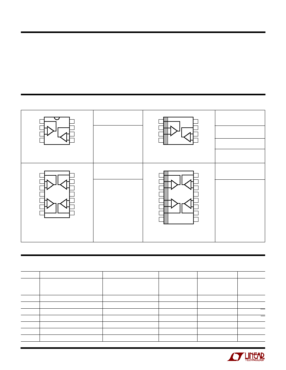
TOP VIEW
A
+IN D
+IN C
≠IN C
C
B
N PACKAGE
14-LEAD PDIP
8
7
6
5
4
3
2
1
≠IN A
+IN A
V
+
TOP VIEW
N8 PACKAGE
8-LEAD PDIP
OUT A
OUT B
V
≠
≠IN B
+IN B
A
B
V
+
D
16
15
14
13
12
11
10
7
6
5
4
3
2
1
OUT A
≠IN A
+IN A
+IN B
≠IN B
OUT B
OUT C
9
8
NC
NC
V
≠
≠IN D
OUT D
TOP VIEW
A
+IN D
+IN C
≠IN C
C
B
S PACKAGE
16-LEAD PLASTIC SO
8
7
6
5
4
3
2
1
≠IN A
+IN A
V
+
TOP VIEW
S8 PACKAGE
8-LEAD PLASTIC SO
OUT A
OUT B
V
≠
≠IN B
+IN B
A
B
(Note 1)
3
LT1355/LT1356
Input Voltage Range
+
±
15V
12.0
13.4
V
±
5V
2.5
3.5
V
±
2.5V
0.5
1.1
V
Input Voltage Range
≠
±
15V
≠13.2
≠12.0
V
±
5V
≠3.4
≠2.5
V
±
2.5V
≠0.9
≠0.5
V
CMRR
Common Mode Rejection Ratio
V
CM
=
±
12V
±
15V
83
97
dB
V
CM
=
±
2.5V
±
5V
78
84
dB
V
CM
=
±
0.5V
±
2.5V
68
75
dB
PSRR
Power Supply Rejection Ratio
V
S
=
±
2.5V to
±
15V
92
106
dB
A
VOL
Large-Signal Voltage Gain
V
OUT
=
±
12V, R
L
= 1k
±
15V
12
36
V/mV
V
OUT
=
±
10V, R
L
= 500
±
15V
5
15
V/mV
V
OUT
=
±
2.5V, R
L
= 1k
±
5V
12
36
V/mV
V
OUT
=
±
2.5V, R
L
= 500
±
5V
5
15
V/mV
V
OUT
=
±
2.5V, R
L
= 150
±
5V
1
4
V/mV
V
OUT
=
±
1V, R
L
= 500
±
2.5V
5
20
V/mV
V
OUT
Output Swing
R
L
= 1k, V
IN
=
±
40mV
±
15V
13.3
13.8
±
V
R
L
= 500
, V
IN
=
±
40mV
±
15V
12.5
13.0
±
V
R
L
= 500
, V
IN
=
±
40mV
±
5V
3.5
4.0
±
V
R
L
= 150
, V
IN
=
±
40mV
±
5V
3.0
3.3
±
V
R
L
= 500
, V
IN
=
±
40mV
±
2.5V
1.3
1.7
±
V
I
OUT
Output Current
V
OUT
=
±
12.5V
±
15V
25
30
mA
V
OUT
=
±
3V
±
5V
20
25
mA
I
SC
Short-Circuit Current
V
OUT
= 0V, V
IN
=
±
3V
±
15V
30
42
mA
SR
Slew Rate
A
V
= ≠ 2, (Note 4)
±
15V
200
400
V/
µ
s
±
5V
70
120
V/
µ
s
Full Power Bandwidth
10V Peak, (Note 5)
±
15V
6.4
MHz
3V Peak, (Note 5)
±
5V
6.4
MHz
GBW
Gain Bandwidth
f = 200kHz, R
L
= 2k
±
15V
9.0
12.0
MHz
±
5V
7.5
10.5
MHz
±
2.5V
9.0
MHz
t
r
, t
f
Rise Time, Fall Time
A
V
= 1, 10%-90%, 0.1V
±
15V
14
ns
±
5V
17
ns
Overshoot
A
V
= 1, 0.1V
±
15V
20
%
±
5V
18
%
Propagation Delay
50% V
IN
to 50% V
OUT
, 0.1V
±
15V
16
ns
±
5V
19
ns
t
s
Settling Time
10V Step, 0.1%, A
V
= ≠1
±
15V
230
ns
10V Step, 0.01%, A
V
= ≠1
±
15V
280
ns
5V Step, 0.1%, A
V
= ≠1
±
5V
240
ns
5V Step, 0.01%, A
V
= ≠1
±
5V
380
ns
Differential Gain
f = 3.58MHz, A
V
= 2, R
L
= 1k
±
15V
2.2
%
±
5V
2.1
%
Differential Phase
f = 3.58MHz, A
V
= 2, R
L
= 1k
±
15V
3.1
Deg
±
5V
3.1
Deg
R
O
Output Resistance
A
V
= 1, f = 100kHz
±
15V
0.7
Channel Separation
V
OUT
=
±
10V, R
L
= 500
±
15V
100
113
dB
I
S
Supply Current
Each Amplifier
±
15V
1.0
1.25
mA
Each Amplifier
±
5V
0.9
1.20
mA
SYMBOL
PARAMETER
CONDITIONS
V
SUPPLY
MIN
TYP
MAX
UNITS
T
A
= 25
∞
C, V
CM
= 0V unless otherwise noted.
ELECTRICAL CHARACTERISTICS

4
LT1355/LT1356
V
OS
Input Offset Voltage
±
15V
q
1.0
mV
±
5V
q
1.0
mV
±
2.5V
q
1.2
mV
Input V
OS
Drift
(Note 6)
±
2.5V to
±
15V
q
5
8
µ
V/
∞
C
I
OS
Input Offset Current
±
2.5V to
±
15V
q
100
nA
I
B
Input Bias Current
±
2.5V to
±
15V
q
450
nA
CMRR
Common Mode Rejection Ratio
V
CM
=
±
12V
±
15V
q
81
dB
V
CM
=
±
2.5V
±
5V
q
77
dB
V
CM
=
±
0.5V
±
2.5V
q
67
dB
PSRR
Power Supply Rejection Ratio
V
S
=
±
2.5V to
±
15V
q
90
dB
A
VOL
Large-Signal Voltage Gain
V
OUT
=
±
12V, R
L
= 1k
±
15V
q
10.0
V/mV
V
OUT
=
±
10V, R
L
= 500
±
15V
q
3.3
V/mV
V
OUT
=
±
2.5V, R
L
= 1k
±
5V
q
10.0
V/mV
V
OUT
=
±
2.5V, R
L
= 500
±
5V
q
3.3
V/mV
V
OUT
=
±
2.5V, R
L
= 150
±
5V
q
0.6
V/mV
V
OUT
=
±
1V, R
L
= 500
±
2.5V
q
3.3
V/mV
V
OUT
Output Swing
R
L
= 1k, V
IN
=
±
40mV
±
15V
q
13.2
±
V
R
L
= 500
, V
IN
=
±
40mV
±
15V
q
12.0
±
V
R
L
= 500
, V
IN
=
±
40mV
±
5V
q
3.4
±
V
R
L
= 150
, V
IN
=
±
40mV
±
5V
q
2.8
±
V
R
L
= 500
, V
IN
=
±
40mV
±
2.5V
q
1.2
±
V
I
OUT
Output Current
V
OUT
=
±
12V
±
15V
q
24.0
mA
V
OUT
=
±
2.8V
±
5V
q
18.7
mA
I
SC
Short-Circuit Current
V
OUT
= 0V, V
IN
=
±
3V
±
15V
q
24
mA
SR
Slew Rate
A
V
= ≠ 2, (Note 4)
±
15V
q
150
V/
µ
s
±
5V
q
60
V/
µ
s
GBW
Gain Bandwidth
f = 200kHz, R
L
= 2k
±
15V
q
7.5
MHz
±
5V
q
6.0
MHz
Channel Separation
V
OUT
=
±
10V, R
L
= 500
±
15V
q
98
dB
I
S
Supply Current
Each Amplifier
±
15V
q
1.45
mA
Each Amplifier
±
5V
q
1.40
mA
SYMBOL
PARAMETER
CONDITIONS
V
SUPPLY
MIN
TYP
MAX
UNITS
ELECTRICAL CHARACTERISTICS
SYMBOL
PARAMETER
CONDITIONS
V
SUPPLY
MIN
TYP
MAX
UNITS
The
q
denotes the specifications which apply over the temperature range
0
∞
C
T
A
70
∞
C, V
CM
= 0V unless otherwise noted.
The
q
denotes the specifications which apply over the temperature range ≠ 40
∞
C
T
A
85
∞
C, V
CM
= 0V unless otherwise noted. (Note 8)
V
OS
Input Offset Voltage
±
15V
q
1.5
mV
±
5V
q
1.5
mV
±
2.5V
q
1.7
mV
Input V
OS
Drift
(Note 6)
±
2.5V to
±
15V
q
5
8
µ
V/
∞
C
I
OS
Input Offset Current
±
2.5V to
±
15V
q
200
nA
I
B
Input Bias Current
±
2.5V to
±
15V
q
550
nA
CMRR
Common Mode Rejection Ratio
V
CM
=
±
12V
±
15V
q
80
dB
V
CM
=
±
2.5V
±
5V
q
76
dB
V
CM
=
±
0.5V
±
2.5V
q
66
dB
PSRR
Power Supply Rejection Ratio
V
S
=
±
2.5V to
±
15V
q
90
dB
A
VOL
Large-Signal Voltage Gain
V
OUT
=
±
12V, R
L
= 1k
±
15V
q
7.0
V/mV
V
OUT
=
±
10V, R
L
= 500
±
15V
q
1.7
V/mV
V
OUT
=
±
2.5V, R
L
= 1k
±
5V
q
7.0
V/mV
V
OUT
=
±
2.5V, R
L
= 500
±
5V
q
1.7
V/mV
5
LT1355/LT1356
SYMBOL
PARAMETER
CONDITIONS
V
SUPPLY
MIN
TYP
MAX
UNITS
ELECTRICAL CHARACTERISTICS
V
OUT
=
±
2.5V, R
L
= 150
±
5V
q
0.4
V/mV
V
OUT
=
±
1V, R
L
= 500
±
2.5V
q
1.7
V/mV
V
OUT
Output Swing
R
L
= 1k, V
IN
=
±
40mV
±
15V
q
13.0
±
V
R
L
= 500
, V
IN
=
±
40mV
±
15V
q
11.5
±
V
R
L
= 500
, V
IN
=
±
40mV
±
5V
q
3.4
±
V
R
L
= 150
, V
IN
=
±
40mV
±
5V
q
2.6
±
V
R
L
= 500
, V
IN
=
±
40mV
±
2.5V
q
1.2
±
V
I
OUT
Output Current
V
OUT
=
±
11.5V
±
15V
q
23.0
mA
V
OUT
=
±
2.6V
±
5V
q
17.3
mA
I
SC
Short-Circuit Current
V
OUT
= 0V, V
IN
=
±
3V
±
15V
q
23
mA
SR
Slew Rate
A
V
= ≠ 2, (Note 4)
±
15V
q
120
V/
µ
s
±
5V
q
50
V/
µ
s
GBW
Gain Bandwidth
f = 200kHz, R
L
= 2k
±
15V
q
7.0
MHz
±
5V
q
5.5
MHz
Channel Separation
V
OUT
=
±
10V, R
L
= 500
±
15V
q
98
dB
I
S
Supply Current
Each Amplifier
±
15V
q
1.50
mA
Each Amplifier
±
5V
q
1.45
mA
Note 1: Absolute Maximum Ratings are those values beyond which the life
of a device may be impaired.
Note 2: Differential inputs of
±
10V are appropriate for transient operation
only, such as during slewing. Large, sustained differential inputs will cause
excessive power dissipation and may damage the part. See Input
Considerations in the Applications Information section of this data sheet
for more details.
Note 3: A heat sink may be required to keep the junction temperature
below absolute maximum when the output is shorted indefinitely.
Note 4: Slew rate is measured between
±
10V on the output with
±
6V input
for
±
15V supplies and
±
1V on the output with
±
1.75V input for
±
5V
supplies.
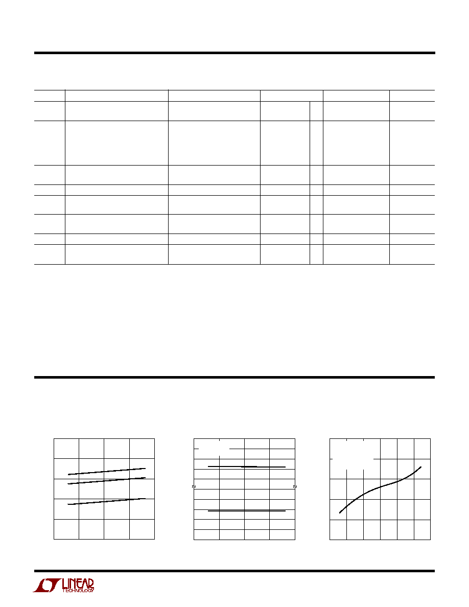
TYPICAL PERFOR
M
A
N
CE CHARACTERISTICS
U
W
Input Common Mode Range vs
Supply Voltage
Supply Current vs Supply Voltage
and Temperature
SUPPLY VOLTAGE (
±
V)
V
≠
COMMON MODE RANGE (V)
2.0
0.5
1.0
1.5
V
+
≠1.0
≠ 0.5
≠2.0
≠1.5
10
5
0
15
20
1355/1356 G02
T
A
= 25
∞
C
V
OS
< 1mV
Input Bias Current vs
Input Common Mode Voltage
INPUT COMMON MODE VOLTAGE (V)
≠50
INPUT BIAS CURRENT (nA)
0
200
150
100
50
≠15
≠10
0
10
15
5
≠5
1355/1356 G03
V
S
=
±
15V
T
A
= 25
∞
C
I
B
=
I
B
+ + I
B
≠
--------
2
Note 5: Full power bandwidth is calculated from the slew rate
measurement: FPBW = (SR)/2
V
P
.
Note 6: This parameter is not 100% tested.
Note 7: The LT1355C/LT1356C are guaranteed functional over the
operating temperature range of ≠40
∞
C to 85
∞
C.
Note 8: The LT1355C/LT1356C are guaranteed to meet specified
performance from 0
∞
C to 70
∞
C. The LT1355C/LT1356C are designed,
characterized and expected to meet specified performance from ≠ 40
∞
C to
85
∞
C, but are not tested or QA sampled at these temperatures. For
guaranteed I-grade parts, consult the factory.
The
q
denotes the specifications which apply over the temperature range
≠ 40
∞
C
T
A
85
∞
C, V
CM
= 0V unless otherwise noted. (Note 8)
SUPPLY VOLTAGE (
±
V)
0.4
SUPPLY CURRENT (mA)
0.8
0.6
1.4
1.2
1.0
10
5
0
15
20
1355/1356 G01
≠ 55
∞
C
25
∞
C
125
∞
C