 | ÐлекÑÑоннÑй компоненÑ: LT1373CS8 | СкаÑаÑÑ:  PDF PDF  ZIP ZIP |
Äîêóìåíòàöèÿ è îïèñàíèÿ www.docs.chipfind.ru
1
LT1373
250kHz Low Supply Current
High Efficiency
1.5A Switching Regulator
s
Boost Regulators
s
CCFL Backlight Driver
s
Laptop Computer Supplies
s
Multiple Output Flyback Supplies
s
Inverting Supplies
The LT
®
1373 is a low supply current high frequency
current mode switching regulator. It can be operated in all
standard switching configurations including boost, buck,
flyback, forward, inverting and "Cuk." A 1.5A high effi-
ciency switch is included on the die, along with all oscilla-
tor, control and protection circuitry. All functions of the
LT1373 are integrated into 8-pin SO/PDIP packages.
Compared to the 500kHz LT1372, which draws 4mA of
quiescent current, the LT1373 switches at 250kHz, typi-
cally consumes only 1mA and has higher efficiency. High
frequency switching allows for small inductors to be used.
All surface mount components consume less than 0.6
square inch of board space.
New design techniques increase flexibility and maintain
ease of use. Switching is easily synchronized to an exter-
nal logic level source. A logic low on the shutdown pin
reduces supply current to 12
µ
A. Unique error amplifier
circuitry can regulate positive or negative output voltage
while maintaining simple frequency compensation tech-
niques. Nonlinear error amplifier transconductance re-
duces output overshoot on start-up or overload recovery.
Oscillator frequency shifting protects external compo-
nents during overload conditions.
s
1mA I
Q
at 250kHz
s
Uses Small Inductors: 15
µ
H
s
All Surface Mount Components
s
Only 0.6 Square Inch of Board Space
s
Low Minimum Supply Voltage: 2.7V
s
Constant Frequency Current Mode
s
Current Limited Power Switch: 1.5A
s
Regulates Positive or Negative Outputs
s
Shutdown Supply Current: 12
µ
A Typ
s
Easy External Synchronization
s
8-Pin SO or PDIP Packages
, LTC and LT are registered trademarks of Linear Technology Corporation.
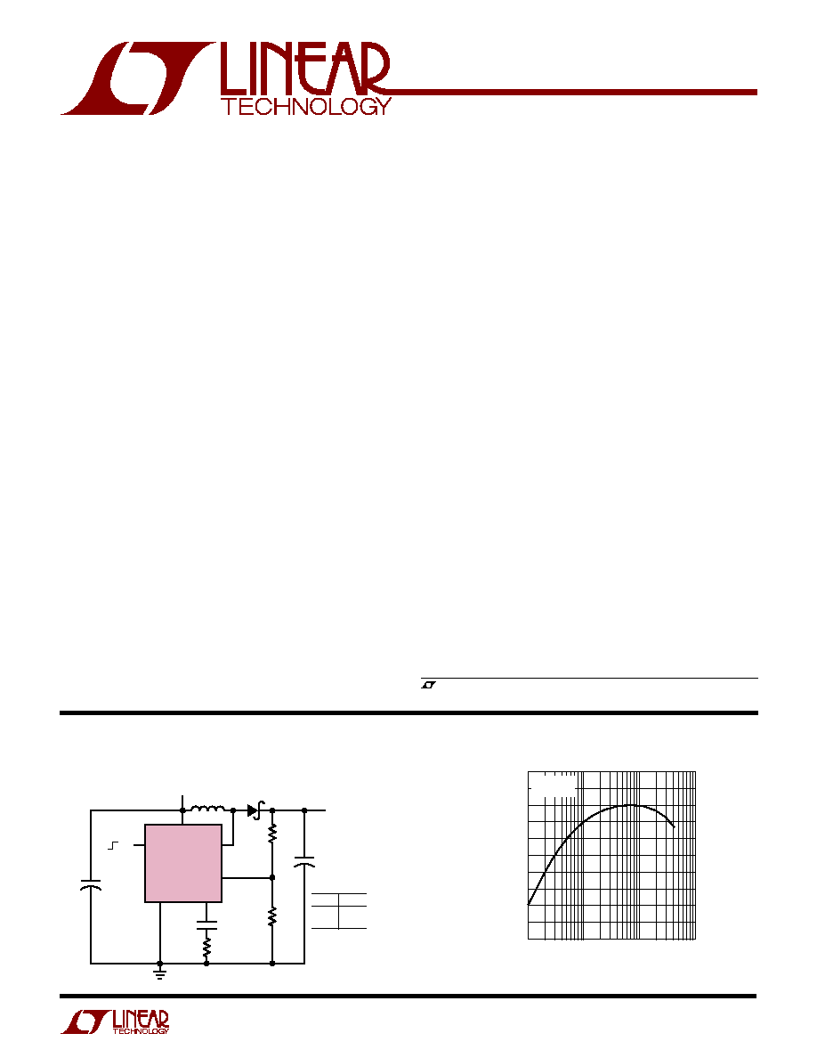
OUTPUT CURRENT (mA)
1
70
EFFICIENCY (%)
80
90
10
100
1000
LT1373 · TA02
60
50
100
V
IN
= 5V
f = 250kHz
LT1373
V
IN
V
C
5V
1
2
8
5
4
6, 7
SUMIDA CD75-220KC (22
µ
H) OR
COILCRAFT D03316-153 (15
µ
H)
AVX TPSD226M025R0200
GND
FB
LT1373 · TA01
V
SW
S/S
L1*
22
µ
H
C1**
22
µ
F
C4**
22
µ
F
C2
0.01
µ
F
R3
5k
R2
24.9k
1%
R1
215k
1%
*
**
V
OUT
12V
MAX I
OUT
D1
MBRS120T3
ON
OFF
L1
15
µ
H
22
µ
H
I
OUT
0.3A
0.35A
+
+
5V-to-12V Boost Converter
12V Output Efficiency
FEATURES
DESCRIPTIO
U
APPLICATIO S
U
TYPICAL APPLICATIO
U
2
LT1373
Consult factory for Military grade parts.
(Note 1)
Supply Voltage ....................................................... 30V
Switch Voltage
LT1373 ............................................................... 35V
LT1373HV .......................................................... 42V
S/S Pin Voltage ....................................................... 30V
Feedback Pin Voltage (Transient, 10ms) ..............
±
10V
Feedback Pin Current ........................................... 10mA
Negative Feedback Pin Voltage
(Transient, 10ms) .............................................
±
10V
Operating Junction Temperature Range
Commercial ........................................ 0
°
C to 125
°
C*
Industrial ......................................... 40
°
C to 125
°
C
Short Circuit ......................................... 0
°
C to 150
°
C
Storage Temperature Range ................ 65
°
C to 150
°
C
Lead Temperature (Soldering, 10 sec)................. 300
°
C
LT1373CN8
LT1373HVCN8
LT1373CS8
LT1373HVCS8
LT1373IN8
LT1373HVIN8
LT1373IS8
LT1373HVIS8
S8 PART MARKING
ORDER PART
NUMBER
1373H
1373HI
1373
1373I
*Units shipped prior to Date Code 9552 are rated at 100
°
C maximum
operating temperature.
SYMBOL
PARAMETER
CONDITIONS
MIN
TYP
MAX
UNITS
V
REF
Reference Voltage
Measured at Feedback Pin
1.230
1.245
1.260
V
V
C
= 0.8V
q
1.225
1.245
1.265
V
I
FB
Feedback Input Current
V
FB
= V
REF
50
150
nA
q
275
nA
Reference Voltage Line Regulation
2.7V
V
IN
25V, V
C
= 0.8V
q
0.01
0.03
%/V
V
NFB
Negative Feedback Reference Voltage
Measured at Negative Feedback Pin
2.51
2.45
2.39
V
Feedback Pin Open, V
C
= 0.8V
q
2.55
2.45
2.35
V
I
NFB
Negative Feedback Input Current
V
NFB
= V
NFR
q
12
7
2
µ
A
Negative Feedback Reference Voltage
2.7V
V
IN
25V, V
C
= 0.8V
q
0.01
0.05
%/V
Line Regulation
g
m
Error Amplifier Transconductance
I
C
=
±
5
µ
A
250
375
500
µ
mho
q
150
600
µ
mho
Error Amplifier Source Current
V
FB
= V
REF
150mV, V
C
= 1.5V
q
25
50
90
µ
A
Error Amplifier Sink Current
V
FB
= V
REF
+ 150mV, V
C
= 1.5V
q
850
1500
µ
A
Error Amplifier Clamp Voltage
High Clamp, V
FB
= 1V
1.70
1.95
2.30
V
Low Clamp, V
FB
= 1.5V
0.25
0.40
0.52
V
A
V
Error Amplifier Voltage Gain
250
V/ V
V
C
Pin Threshold
Duty Cycle = 0%
0.8
1
1.25
V
f
Switching Frequency
2.7V
V
IN
25V
225
250
275
kHz
0
°
C
T
J
125
°
C
q
210
250
290
kHz
40
°
C
T
J
0
°
C (I Grade)
200
290
kHz
Maximum Switch Duty Cycle
q
90
95
%
Switch Current Limit Blanking Time
340
500
ns
The
q
denotes specifications which apply over the full operating temperature range, otherwise specifications are at T
A
= 25
°
C.
V
IN
= 5V, V
C
= 0.6V, V
FB
= V
REF
, V
SW
, S/S and NFB pins open, unless otherwise noted.
1
2
3
4
8
7
6
5
TOP VIEW
V
C
FB
NFB
S/S
V
SW
GND
GND S
V
IN
N8 PACKAGE
8-LEAD PDIP
S8 PACKAGE
8-LEAD PLASTIC SO
T
JMAX
= 125
°
C,
JA
= 100
°
C/ W (N8)
T
JMAX
= 125
°
C,
JA
= 120
°
C/ W (S8)
ABSOLUTE AXI U RATI GS
W
W
W
U
PACKAGE/ORDER I FOR ATIO
U
U
W
ELECTRICAL CHARACTERISTICS
3
LT1373
SYMBOL
PARAMETER
CONDITIONS
MIN
TYP
MAX
UNITS
BV
Output Switch Breakdown Voltage
LT1373
q
35
47
V
LT1373HV
0
°
C
T
J
125
°
C
q
42
47
V
40
°
C
T
J
0
°
C (I Grade)
40
V
V
SAT
Output Switch "On" Resistance
I
SW
= 1A
q
0.5
0.85
I
LIM
Switch Current Limit
Duty Cycle = 50%
q
1.5
1.9
2.7
A
Duty Cycle = 80% (Note 2)
q
1.3
1.7
2.5
A
I
IN
Supply Current Increase During Switch On-Time
10
20
mA/A
I
SW
Control Voltage to Switch Current
2
A/V
Transconductance
Minimum Input Voltage
q
2.4
2.7
V
I
Q
Supply Current
2.7V
V
IN
25V
q
1
1.5
mA
Shutdown Supply Current
2.7V
V
IN
25V, V
S/S
0.6V
0
°
C
T
J
125
°
C
q
12
30
µ
A
40
°
C
T
J
0
°
C (I Grade)
50
µ
A
Shutdown Threshold
2.7V
V
IN
25V
q
0.6
1.3
2
V
Shutdown Delay
q
5
12
100
µ
s
S/S Pin Input Current
0V
V
S/S
5V
q
10
15
µ
A
Synchronization Frequency Range
q
300
340
kHz
Note 1: Absolute Maximum Ratings are those values beyond which the life
of the device may be impaired.
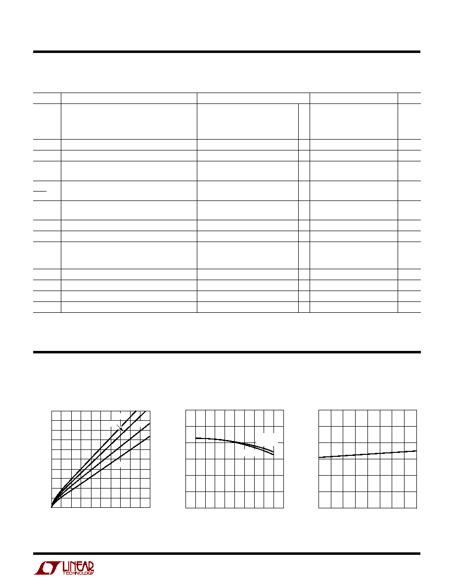
SWITCH CURRENT (A)
0
SWITCH SATURATION VOLTAGE (V)
0.6
0.8
1.0
1.6
LT1373 · G01
0.4
0.2
0.5
0.7
0.9
0.3
0.1
0
0.4
0.8
1.2
2.0
1.4
0.2
0.6
1.0
1.8
100
°
C
150
°
C
25
°
C
55
°
C
Switch Saturation Voltage
vs Switch Current
TEMPERATURE (
°
C)
50
1.8
INPUT VOLTAGE (V)
2.0
2.2
2.4
2.6
0
50
100
150
LT1373 · G03
2.8
3.0
25
25
75
125
Minimum Input Voltage
vs Temperature
DUTY CYCLE (%)
0
SWITCH CURRENT LIMIT (A)
1.0
2.0
3.0
0.5
1.5
2.5
20
40
60
80
LT1373 · G02
100
10
0
30
50
70
90
25
°
C AND
125
°
C
55
°
C
Switch Current Limit
vs Duty Cycle
The
q
denotes specifications which apply over the full operating temperature range, otherwise specifications are at T
A
= 25
°
C.
V
IN
= 5V, V
C
= 0.6V, V
FB
= V
REF
, V
SW
, S/S and NFB pins open, unless otherwise noted.
ELECTRICAL CHARACTERISTICS
Note 2: For duty cycles (DC) between 50% and 90%, minimum
guaranteed switch current is given by I
LIM
= 0.667 (2.75 DC).
TYPICAL PERFOR A CE CHARACTERISTICS
U
W
4
LT1373
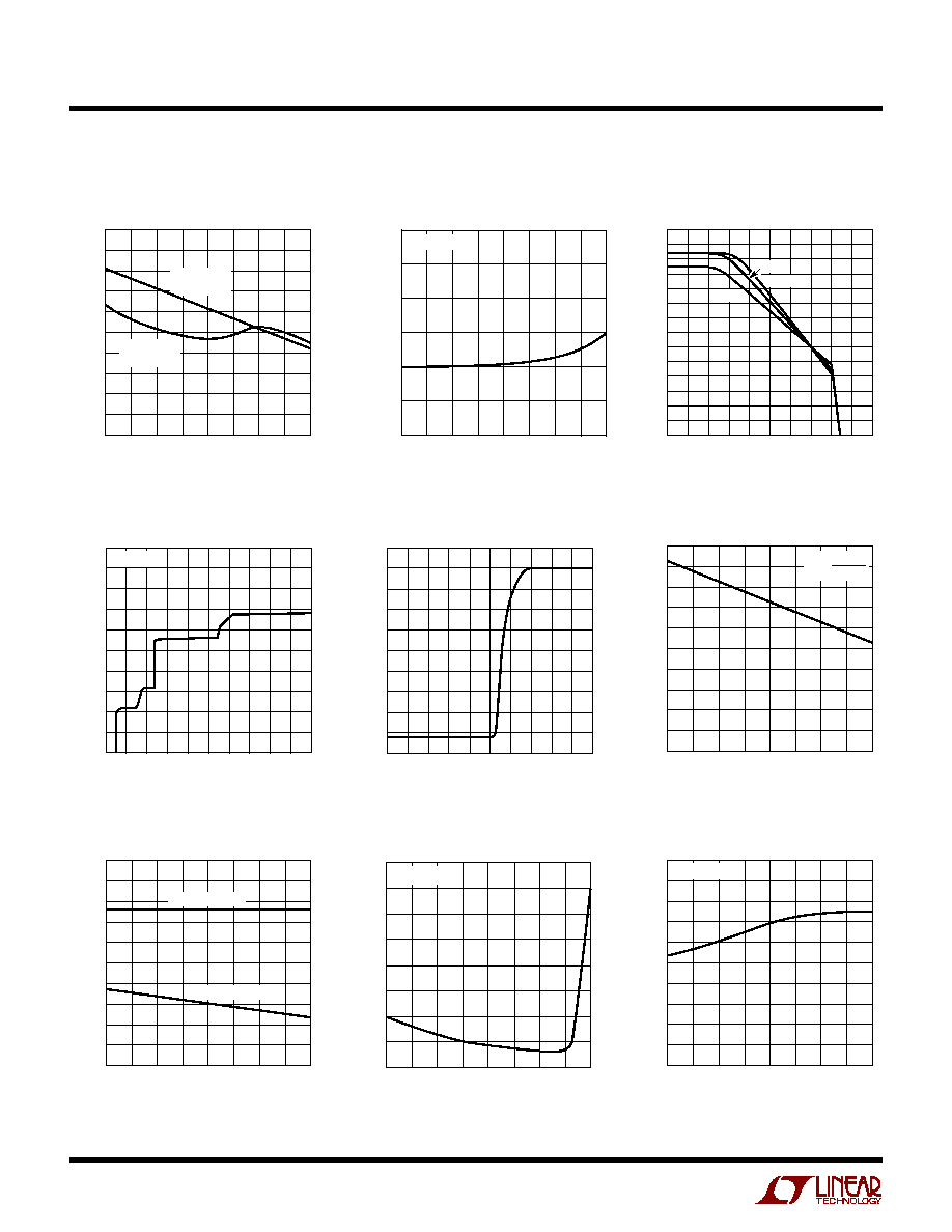
Shutdown Delay and Threshold
vs Temperature
Error Amplifier Output Current
vs Feedback Pin Voltage
TEMPERATURE (
°
C)
50
0
SHUTDOWN DELAY (
µ
s)
SHUTDOWN THRESHOLD (V)
2
6
8
10
20
14
0
50
75
LT1373 · G04
4
16
18
12
0
0.2
0.6
0.8
1.0
2.0
1.4
0.4
1.6
1.8
1.2
25
25
100 125
150
SHUTDOWN
THRESHOLD
SHUTDOWN
DELAY
TEMPERATURE (
°
C)
50
0
MINIMUM SYNCHRONIZATION VOLTAGE (V
P-P
)
0.5
1.0
1.5
2.0
0
50
100
150
LT1373 · G05
2.5
3.0
25
25
75
125
f
SYNC
= 330kHz
Minimum Synchronization
Voltage vs Temperature
FEEDBACK PIN VOLTAGE (V)
100
ERROR AMPLIFIER OUTPUT CURRENT (
µ
A)
75
50
25
75
25
0.1
0.1
50
0
0.3
0.2
V
REF
55
°
C
125
°
C
25
°
C
LT1373 · G06
S/S Pin Input Current
vs Voltage
S/S PIN VOLTAGE (V)
1
S/S PIN INPUT CURRENT (
µ
A)
1
3
5
7
LT1373 · G07
1
3
0
2
4
2
4
5
1
3
5
0
8
2
4
6
9
V
IN
= 5V
Error Amplifier Transconductance
vs Temperature
Switching Frequency
vs Feedback Pin Voltage
FEEDBACK PIN VOLTAGE (V)
0
SWITCHING FREQUENCY (% OF TYPICAL)
70
90
110
0.8
LT1373 · G08
50
30
60
80
100
40
20
10
0.2
0.4
0.6
0.1
0.9
0.3
0.5
0.7
1.0
TEMPERATURE (
°
C)
50
0
TRANSCONDUCTANCE (
µ
mho)
200
500
0
50
75
LT1373 · G09
100
400
300
25
25
100 125
150
g
m
=
I (V
C
)
V (FB)
V
C
Pin Threshold and High
Clamp Voltage vs Temperature
Negative Feedback Input
Current vs Temperature
Feedback Input Current
vs Temperature
TEMPERATURE (
°
C)
50
0.4
V
C
PIN VOLTAGE (V)
0.6
1.0
1.2
1.4
2.4
1.8
0
50
75
LT1373 · G10
0.8
2.0
2.2
1.6
25
25
100 125
150
V
C
HIGH CLAMP
V
C
THRESHOLD
TEMPERATURE (
°
C)
50
FEEDBACK INPUT CURRENT (nA)
200
250
300
150
LT1373 · G11
150
100
0
0
50
100
50
400
350
25
25
75
125
V
FB
= V
REF
TEMPERATURE (
°
C)
50
20
NEGATIVE FEEDBACK INPUT CURRENT (
µ
A)
12
14
0
0
50
75
LT1373 · G12
16
18
4
6
2
8
10
25
25
100 125
150
V
NFB
= V
NFR
TYPICAL PERFOR A CE CHARACTERISTICS
U
W
5
LT1373
V
C
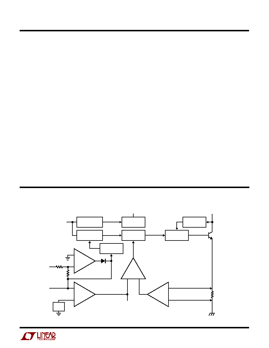
(Pin 1): Compensation Pin. The V
C
pin is used for
frequency compensation, current limiting and soft start. It
is the output of the error amplifier and the input of the
current comparator. Loop frequency compensation can be
performed with an RC network connected from the V
C
pin
to ground.
FB (Pin 2): The feedback pin is used for positive output
voltage sensing and oscillator frequency shifting. It is the
inverting input to the error amplifier. The noninverting
input of this amplifier is internally tied to a 1.245V
reference. Load on the FB pin should not exceed 100
µ
A
when the NFB pin is used. See Applications Information.
NFB (Pin 3): The negative feedback pin is used for negative
output voltage sensing. It is connected to the inverting
input of the negative feedback amplifier through a 400k
source resistor.
S/S (Pin 4): Shutdown and Synchronization Pin. The S/S
pin is logic level compatible. Shutdown is active low and
the shutdown threshold is typically 1.3V. For normal
operation, pull the S/S pin high, tie it to V
IN
or leave it
floating. To synchronize switching, drive the S/S pin be-
tween 300kHz and 340kHz.
V
IN
(Pin 5): Input Supply Pin. Bypass V
IN
with 10
µ
F or
more. The part goes into undervoltage lockout when V
IN
drops below 2.5V. Undervoltage lockout stops switching
and pulls the V
C
pin low.
GND S (Pin 6): The ground sense pin is a "clean" ground.
The internal reference, error amplifier and negative feed-
back amplifier are referred to the ground sense pin. Con-
nect it to ground. Keep the ground path connection to the
output resistor divider and the V
C
compensation network
free of large ground currents.
GND (Pin 7): The ground pin is the emitter connection of
the power switch and has large currents flowing through it.
It should be connected directly to a good quality ground
plane.
V
SW
(Pin 8): The switch pin is the collector of the power
switch and has large currents flowing through it. Keep the
traces to the switching components as short as possible to
minimize radiation and voltage spikes.
+
NEGATIVE
FEEDBACK
AMP
NFB
S/S
FB
400k
200k
0.08
+
V
C
V
IN
GND
LT1373 · BD
GND SENSE
1.245V
REF
5:1 FREQUENCY
SHIFT
250kHz
OSC
SYNC
SHUTDOWN
DELAY AND RESET
LOW DROPOUT
2.3V REG
ANTI-SAT
LOGIC
DRIVER
SW
SWITCH
+
A
V
6
COMP
ERROR
AMP
CURRENT
AMP
U
U
U
PI FU CTIO S
BLOCK DIAGRA
W