 | –≠–ª–µ–∫—Ç—Ä–æ–Ω–Ω—ã–π –∫–æ–º–ø–æ–Ω–µ–Ω—Ç: LT1398 | –°–∫–∞—á–∞—Ç—å:  PDF PDF  ZIP ZIP |
1
LT1398/LT1399/LT1399HV
Low Cost Dual and Triple
300MHz Current Feedback
Amplifiers with Shutdown
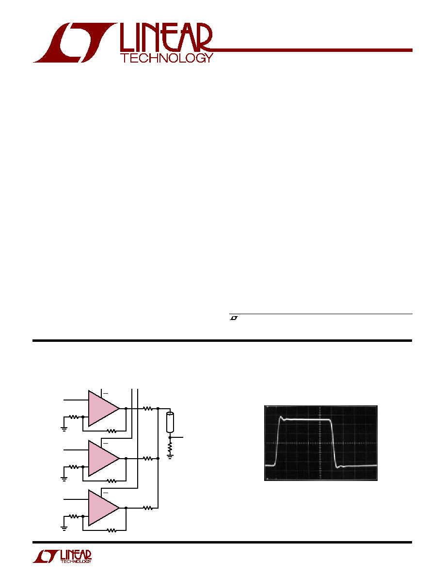
3-Input Video MUX Cable Driver
The LT
Æ
1399 and LT1399HV contain three independent
300MHz current feedback amplifiers, each with a shut-
down pin. The LT1399HV is a higher voltage version of the
LT1399. The LT1398 is a two amplifier version of the
LT1399.
The LT1398/LT1399 operate on all supplies from a single
4V to
±
6V. The LT1399HV operates on all supplies from 4V
to
±
7.5V.
Each amplifier draws 4.6mA when active. When disabled
each amplifier draws zero supply current and its output be-
comes high impedance. The amplifiers turn on in only 30ns
and turn off in 40ns, making them ideal in spread spectrum
and portable equipment applications.
The LT1398/LT1399/LT1399HV are manufactured on Lin-
ear Technology's proprietary complementary bipolar pro-
cess. The LT1399/LT1399HV are pin-for-pin upgrades to
the LT1260 optimized for use on
±
5V/
±
7.5V supplies.
s
300MHz Bandwidth on
±
5V (A
V
= 1, 2 and ≠1)
s
0.1dB Gain Flatness: 150MHz (A
V
= 1, 2 and ≠1)
s
Completely Off in Shutdown, 0
µ
A Supply Current
s
High Slew Rate: 800V/
µ
s
s
Wide Supply Range:
±
2V(4V) to
±
6V(12V) (LT1398/LT1399)
±
2V (4V) to
±
7.5V (15V) (LT1399HV)
s
80mA Output Current
s
Low Supply Current: 4.6mA/Amplifier
s
Fast Turn-On Time: 30ns
s
Fast Turn-Off Time: 40ns
s
16-Pin Narrow SO/Narrow SSOP Packages
s
RGB Cable Drivers
s
LCD Drivers
s
Spread Spectrum Amplifiers
s
MUX Amplifiers
s
Composite Video Cable Drivers
s
Portable Equipment
, LTC and LT are registered trademarks of Linear Technology Corporation.
Square Wave Response
OUTPUT
200mV/DIV
TIME (10ns/DIV)
1398/99 TA02
R
L
= 100
R
F
= R
G
= 324
f = 10MHz
FEATURES
DESCRIPTIO
U
APPLICATIO S
U
TYPICAL APPLICATIO
U
≠
+
1/3 LT1399
R
G
200
R
F
324
A
EN A
V
IN A
≠
+
1/3 LT1399
R
G
200
R
F
324
EN B
V
IN B
B C
CHANNEL
SELECT
97.6
97.6
≠
+
1/3 LT1399
R
G
200
R
F
324
EN C
V
IN C
97.6
75
V
OUT
75
CABLE
1399 TA01
2
LT1398/LT1399/LT1399HV
The
q
denotes specifications which apply over the specified operating temperature range, otherwise specifications are at T
A
= 25
∞
C.
For each amplifier: V
CM
= 0V, V
S
=
±
5V, EN = 0V, pulse tested, unless otherwise noted. (Note 4)
A
U
G
W
A
W
U
W
A
R
BSOLUTE
XI
TI
S
(Note 1)
Total Supply Voltage (V
+
to V
≠
)
LT1398/LT1399 ................................................ 12.6V
LT1399HV ....................................................... 15.5V
Input Current (Note 2) .......................................
±
10mA
Output Current .................................................
±
100mA
Differential Input Voltage (Note 2) ...........................
±
5V
Output Short-Circuit Duration (Note 3) ........ Continuous
Operating Temperature Range ............... ≠ 40
∞
C to 85
∞
C
Specified Temperature Range (Note 4) .. ≠ 40
∞
C to 85
∞
C
Storage Temperature Range ................ ≠ 65
∞
C to 150
∞
C
Junction Temperature (Note 5) ............................ 150
∞
C
Lead Temperature (Soldering, 10 sec)................. 300
∞
C
W
U
U
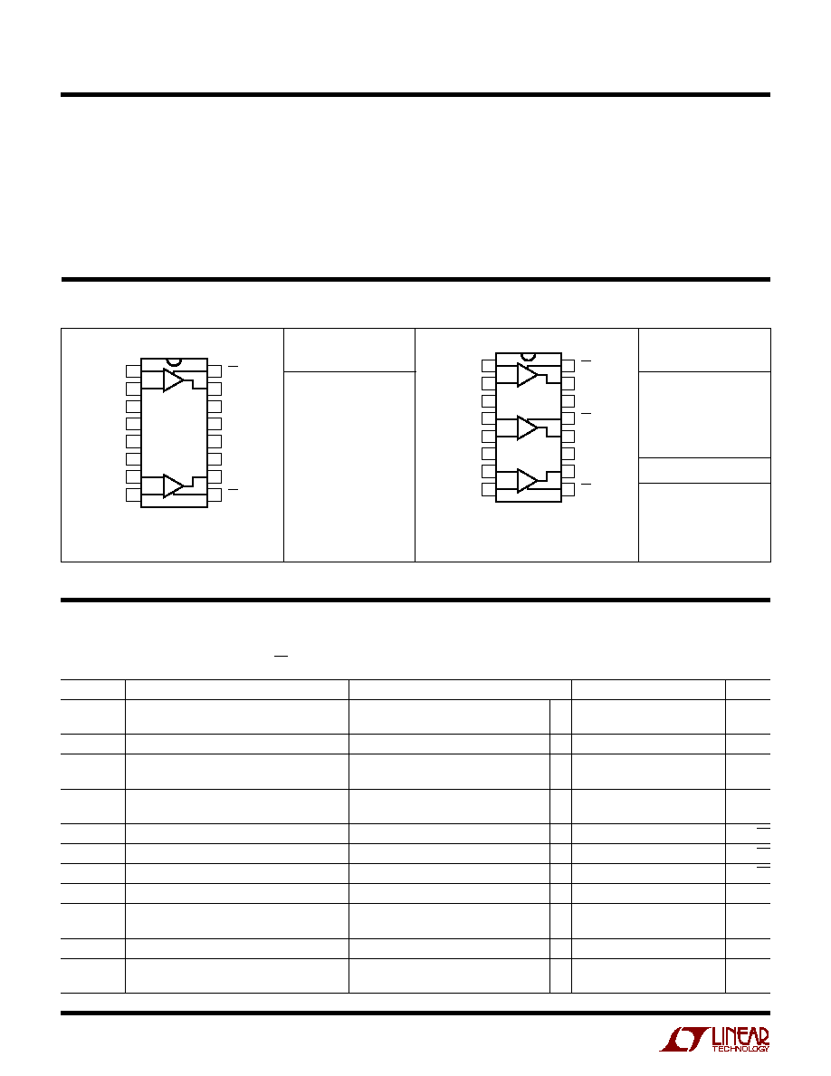
PACKAGE/ORDER I FOR ATIO
ORDER PART
NUMBER
LT1399CGN
LT1399CS
LT1399HVCS
T
JMAX
= 150
∞
C,
JA
= 120
∞
C/W (GN)
T
JMAX
= 150
∞
C,
JA
= 100
∞
C/W (S)
*Ground pins are not internally connected. For best channel isolation, connect to ground. Consult factory for Industrial and Military grade parts.
ORDER PART
NUMBER
LT1398CS
T
JMAX
= 150
∞
C,
JA
= 100
∞
C/W
1
2
3
4
5
6
7
8
TOP VIEW
16
15
14
13
12
11
10
9
≠IN A
+IN A
*GND
*GND
*GND
*GND
+IN B
≠IN B
EN A
OUT A
V
+
GND*
GND*
V
≠
OUT B
EN B
A
S PACKAGE
16-LEAD PLASTIC SO
B
ELECTRICAL C
C
HARA TERISTICS
SYMBOL
PARAMETER
CONDITIONS
MIN
TYP
MAX
UNITS
V
OS
Input Offset Voltage
1.5
10
mV
q
12
mV
V
OS
/
T
Input Offset Voltage Drift
q
15
µ
V/
∞
C
I
IN
+
Noninverting Input Current
10
25
µ
A
q
30
µ
A
I
IN
≠
Inverting Input Current
10
50
µ
A
q
60
µ
A
e
n
Input Noise Voltage Density
f = 1kHz, R
F
= 1k, R
G
= 10
, R
S
= 0
4.5
nV/
Hz
+ i
n
Noninverting Input Noise Current Density
f = 1kHz
6
pA/
Hz
≠ i
n
Inverting Input Noise Current Density
f = 1kHz
25
pA/
Hz
R
IN
Input Resistance
V
IN
=
±
3.5V
q
0.3
1
M
C
IN
Input Capacitance
Amplifier Enabled
2.0
pF
Amplifier Disabled
2.5
pF
C
OUT
Output Capacitance
Amplifier Disabled
8.5
pF
V
INH
Input Voltage Range, High
V
S
=
±
5V
q
3.5
4.0
V
V
S
= 5V, 0V
4.0
V
1
2
3
4
5
6
7
8
TOP VIEW
16
15
14
13
12
11
10
9
≠IN R
+IN R
*GND
≠IN G
+IN G
*GND
+IN B
≠IN B
EN R
OUT R
V
+
EN G
OUT G
V
≠
OUT B
EN B
R
G
S PACKAGE
16-LEAD PLASTIC SO
GN PACKAGE
16-LEAD PLASTIC SSOP
B
GN PART MARKING
1399
(LT1398/LT1399)
3
LT1398/LT1399/LT1399HV
ELECTRICAL C
C
HARA TERISTICS
SYMBOL
PARAMETER
CONDITIONS
MIN
TYP
MAX
UNITS
V
INL
Input Voltage Range, Low
V
S
=
±
5V
q
≠ 3.5
≠ 4.0
V
V
S
= 5V, 0V
1.0
V
V
OUTH
Maximum Output Voltage Swing, High
V
S
=
±
5V, R
L
= 100k
3.9
4.2
V
V
S
=
±
5V, R
L
= 100k
q
3.7
V
V
S
= 5V, 0V; R
L
= 100k
4.2
V
V
OUTL
Maximum Output Voltage Swing, Low
V
S
=
±
5V, R
L
= 100k
≠ 3.9
≠ 4.2
V
V
S
=
±
5V, R
L
= 100k
q
≠ 3.7
V
V
S
= 5V, 0V; R
L
= 100k
0.8
V
V
OUTH
Maximum Output Voltage Swing, High
V
S
=
±
5V, R
L
= 150
3.4
3.6
V
V
S
=
±
5V, R
L
= 150
q
3.2
V
V
S
= 5V, 0V; R
L
= 150
3.6
V
V
OUTL
Maximum Output Voltage Swing, Low
V
S
=
±
5V, R
L
= 150
≠ 3.4
≠ 3.6
V
V
S
=
±
5V, R
L
= 150
q
≠ 3.2
V
V
S
= 5V, 0V; R
L
= 150
0.6
V
CMRR
Common Mode Rejection Ratio
V
CM
=
±
3.5V
q
42
52
dB
≠ I
CMRR
Inverting Input Current
V
CM
=
±
3.5V
10
16
µ
A/V
Common Mode Rejection
V
CM
=
±
3.5V
q
22
µ
A/V
PSRR
Power Supply Rejection Ratio
V
S
=
±
2V to
±
5V, EN = V
≠
q
56
70
dB
+ I
PSRR
Noninverting Input Current
V
S
=
±
2V to
±
5V, EN = V
≠
1
2
µ
A/V
Power Supply Rejection
q
3
µ
A/V
≠ I
PSRR
Inverting Input Current
V
S
=
±
2V to
±
5V, EN = V
≠
q
2
7
µ
A/V
Power Supply Rejection
A
V
Large-Signal Voltage Gain
V
OUT
=
±
2V, R
L
= 150
50
65
dB
R
OL
Transimpedance,
V
OUT
/
I
IN
≠
V
OUT
=
±
2V, R
L
= 150
40
100
k
I
OUT
Maximum Output Current
R
L
= 0
q
80
mA
I
S
Supply Current per Amplifier
V
OUT
= 0V
q
4.6
6.5
mA
Disable Supply Current per Amplifier
EN Pin Voltage = 4.5V, R
L
= 150
q
0.1
100
µ
A
I
EN
Enable Pin Current
30
110
µ
A
q
200
µ
A
SR
Slew Rate (Note 6)
A
V
= 10, R
L
= 150
500
800
V/
µ
s
t
ON
Turn-On Delay Time (Note 7)
R
F
= R
G
= 324
, R
L
= 100
30
75
ns
t
OFF
Turn-Off Delay Time (Note 7)
R
F
= R
G
= 324
, R
L
= 100
40
100
ns
t
r
, t
f
Small-Signal Rise and Fall Time
R
F
= R
G
= 324
, R
L
= 100
, V
OUT
= 1V
P-P
1.3
ns
t
PD
Propagation Delay
R
F
= R
G
= 324
, R
L
= 100
, V
OUT
= 1V
P-P
2.5
ns
os
Small-Signal Overshoot
R
F
= R
G
= 324
, R
L
= 100
, V
OUT
= 1V
P-P
10
%
t
S
Settling Time
0.1%, A
V
= ≠ 1, R
F
= R
G
= 309
, R
L
= 150
25
ns
dG
Differential Gain (Note 8)
R
F
= R
G
= 324
, R
L
= 150
0.13
%
dP
Differential Phase (Note 8)
R
F
= R
G
= 324
, R
L
= 150
0.10
DEG
The
q
denotes specifications which apply over the specified operating temperature range, otherwise specifications are at T
A
= 25
∞
C.
For each amplifier: V
CM
= 0V, V
S
=
±
5V, EN = 0V, pulse tested, unless otherwise noted. (Note 4)
(LT1398/LT1399)
4
LT1398/LT1399/LT1399HV
The
q
denotes specifications which apply over the specified operating temperature range, otherwise specifications are at T
A
= 25
∞
C.
For each amplifier: V
CM
= 0V, V
S
=
±
7.5V, EN = 0V, pulse tested, unless otherwise noted. (Note 4)
ELECTRICAL C
C
HARA TERISTICS
SYMBOL
PARAMETER
CONDITIONS
MIN
TYP
MAX
UNITS
V
OS
Input Offset Voltage
1.5
10
mV
q
12
mV
V
OS
/
T
Input Offset Voltage Drift
q
15
µ
V/
∞
C
I
IN
+
Noninverting Input Current
10
25
µ
A
q
30
µ
A
I
IN
≠
Inverting Input Current
10
50
µ
A
q
60
µ
A
e
n
Input Noise Voltage Density
f = 1kHz, R
F
= 1k, R
G
= 10
, R
S
= 0
, V
S
=
±
5V
4.5
nV/
Hz
+ i
n
Noninverting Input Noise Current Density
f = 1kHz, V
S
=
±
5V
6
pA/
Hz
≠ i
n
Inverting Input Noise Current Density
f = 1kHz, V
S
=
±
5V
25
pA/
Hz
R
IN
Input Resistance
V
IN
=
±
6V
q
0.3
1
M
C
IN
Input Capacitance
Amplifier Enabled
2.0
pF
Amplifier Disabled
2.5
pF
C
OUT
Output Capacitance
Amplifier Disabled
8.5
pF
V
INH
Input Voltage Range, High
V
S
=
±
7.5V
q
6
6.5
V
V
S
= 7.5V, 0V
6.5
V
V
INL
Input Voltage Range, Low
V
S
=
±
7.5V
q
≠ 6
≠ 6.5
V
V
S
= 7.5V, 0V
1.0
V
V
OUTH
Maximum Output Voltage Swing, High
V
S
=
±
7.5V, R
L
= 100k
6.4
6.7
V
V
S
=
±
7.5V, R
L
= 100k
q
6.1
V
V
S
= 7.5V, 0V; R
L
= 100k
6.7
V
V
OUTL
Maximum Output Voltage Swing, Low
V
S
=
±
7.5V, R
L
= 100k
≠ 6.4
≠ 6.7
V
V
S
=
±
7.5V, R
L
= 100k
q
≠ 6.1
V
V
S
= 7.5V, 0V; R
L
= 100k
0.8
V
V
OUTH
Maximum Output Voltage Swing, High
V
S
=
±
7.5V, R
L
= 150
5.4
5.8
V
V
S
=
±
7.5V, R
L
= 150
q
5.1
V
V
S
= 7.5V, 0V; R
L
= 150
5.8
V
V
OUTL
Maximum Output Voltage Swing, Low
V
S
=
±
7.5V, R
L
= 150
≠ 5.4
≠ 5.8
V
V
S
=
±
7.5V, R
L
= 150
q
≠ 5.1
V
V
S
= 7.5V, 0V; R
L
= 150
0.6
V
CMRR
Common Mode Rejection Ratio
V
CM
=
±
6V
q
42
52
dB
≠ I
CMRR
Inverting Input Current
V
CM
=
±
6V
10
16
µ
A/V
Common Mode Rejection
V
CM
=
±
6V
q
22
µ
A/V
PSRR
Power Supply Rejection Ratio
V
S
=
±
2V to
±
7.5V, EN = V
≠
q
56
70
dB
+ I
PSRR
Noninverting Input Current
V
S
=
±
2V to
±
7.5V, EN = V
≠
1
2
µ
A/V
Power Supply Rejection
q
3
µ
A/V
≠ I
PSRR
Inverting Input Current
V
S
=
±
2V to
±
7.5V, EN = V
≠
q
2
7
µ
A/V
Power Supply Rejection
A
V
Large-Signal Voltage Gain
V
OUT
=
±
4.5V, R
L
= 150
50
65
dB
R
OL
Transimpedance,
V
OUT
/
I
IN
≠
V
OUT
=
±
4.5V, R
L
= 150
40
100
k
I
OUT
Maximum Output Current
R
L
= 0
q
80
mA
I
S
Supply Current per Amplifier
V
OUT
= 0V
q
4.6
7
mA
Disable Supply Current per Amplifier
EN Pin Voltage = 7V, R
L
= 150
q
0.1
100
µ
A
I
EN
Enable Pin Current
30
110
µ
A
q
200
µ
A
(LT1399HV)
5
LT1398/LT1399/LT1399HV
The
q
denotes specifications which apply over the specified operating temperature range, otherwise specifications are at T
A
= 25
∞
C.
For each amplifier: V
CM
= 0V, V
S
=
±
7.5V, EN = 0V, pulse tested, unless otherwise noted. (Note 4)
ELECTRICAL C
C
HARA TERISTICS
SYMBOL
PARAMETER
CONDITIONS
MIN
TYP
MAX
UNITS
SR
Slew Rate (Note 6)
A
V
= 10, R
L
= 150
, V
S
=
±
5V
500
800
V/
µ
s
t
ON
Turn-On Delay Time (Note 7)
R
F
= R
G
= 324
, R
L
= 100
, V
S
=
±
5V
30
75
ns
t
OFF
Turn-Off Delay Time (Note 7)
R
F
= R
G
= 324
, R
L
= 100
, V
S
=
±
5V
40
100
ns
t
r
, t
f
Small-Signal Rise and Fall Time
R
F
= R
G
= 324
, R
L
= 100
, V
OUT
= 1V
P-P
,
1.3
ns
V
S
=
±
5V
t
PD
Propagation Delay
R
F
= R
G
= 324
, R
L
= 100
, V
OUT
= 1V
P-P
,
2.5
ns
V
S
=
±
5V
os
Small-Signal Overshoot
R
F
= R
G
= 324
, R
L
= 100
, V
OUT
= 1V
P-P
,
10
%
V
S
=
±
5V
t
S
Settling Time
0.1%, A
V
= ≠ 1V, R
F
= R
G
= 309
, R
L
= 150
,
25
ns
V
S
=
±
5V
dG
Differential Gain (Note 8)
R
F
= R
G
= 324
, R
L
= 150
, V
S
=
±
5V
0.13
%
dP
Differential Phase (Note 8)
R
F
= R
G
= 324
, R
L
= 150
, V
S
=
±
5V
0.10
DEG
Note 1: Absolute Maximum Ratings are those values beyond which the life
of a device may be impaired.
Note 2: This parameter is guaranteed to meet specified performance
through design and characterization. It has not been tested.
Note 3: A heat sink may be required depending on the power supply
voltage and how many amplifiers have their outputs short circuited.
Note 4: The LT1398/LT1399/LT1399HV are guaranteed to meet specified
performance from 0
∞
C to 70
∞
C and are designed, characterized and
expected to meet these extended temperature limits, but are not tested at
≠ 40
∞
C and 85
∞
C. Guaranteed I grade parts are available, consult factory.
Note 5: T
J
is calculated from the ambient temperature T
A
and the
power dissipation P
D
according to the following formula:
LT1398CS, LT1399CS, LT1399HVCS: T
J
= T
A
+ (P
D
∑ 100
∞
C/W)
LT1399CGN: T
J
= T
A
+ (P
D
∑ 120
∞
C/W)
Note 6: Slew rate is measured at
±
2V on a
±
3V output signal.
Note 7: Turn-on delay time (t
ON
) is measured from control input to
appearance of 1V at the output, for V
IN
= 1V. Likewise, turn-off delay
time (t
OFF
) is measured from control input to appearance of 0.5V on
the output for V
IN
= 0.5V. This specification is guaranteed by design
and characterization.
Note 8: Differential gain and phase are measured using a Tektronix
TSG120YC/NTSC signal generator and a Tektronix 1780R Video
Measurement Set. The resolution of this equipment is 0.1% and 0.1
∞
.
Ten identical amplifier stages were cascaded giving an effective
resolution of 0.01% and 0.01
∞
.
SMALL SIGNAL
SMALL SIGNAL
SMALL SIGNAL
V
S
(V)
A
V
R
L
(
)
R
F
(
)
R
G
(
)
≠ 3dB BW (MHz)
0.1dB BW (MHz)
PEAKING (dB)
±
5
1
100
365
≠
300
150
0.05
±
5
2
100
324
324
300
150
0
±
5
≠ 1
100
309
309
300
150
0
TYPICAL AC PERFOR A CE
W U
(LT1399HV)