1
LT1413
S
FEATURE
Single Supply Operation:
s
Input Goes Below Ground
s
Output Swings to Ground Sinking Current
s
No Pull-Down Resistors Needed
s
Phase Reversal Protection
At 5V, 0V Low Cost Grade Specifications:
s
280
µ
V Max Offset Voltage
s
380
µ
V Max in S8 Package
s
0.8nA Max Offset Current
s
480
µ
A Max Supply Current per Amplifier
s
0.5
µ
V/
∞
C Drift
s
1.4 Million Voltage Gain
s
950kHz Gain-Bandwidth Product
s
0.55
µ
V
P-P
, 0.1Hz to 10Hz Noise
The LT1413 is a low cost, upgraded version of Linear
Technology's industry standard LT1013 dual, single sup-
ply op amp. The LT1413 is optimized for single 5V appli-
cations, although
±
15V specifications are also provided
for completeness.
In the design of the LT1413, particular emphasis has been
placed on low cost plastic and SO-8 package performance:
60
µ
V offset voltage, 0.1nA offset current, in excess of
10mA output current at 330
µ
A supply current and 140dB
channel separation are some of the specifications achieved.
Other dual, single supply amplifiers are available to
complement the LT1413 family: the micropower LT1078's
supply current is 10 times lower with a 4.5 fold speed
performance degradation compared to the LT1413. Con-
versely, the LT1211, LT1213 and LT1215 duals have 4 to
14 times higher supply current, but also 13 to 50 times
higher speed.
Protected by U.S. Patent 4,775,884.
D
U
ESCRIPTIO
Single Supply, Dual
Precision Op Amp
U
S
A
O
PPLICATI
s
Single Supply Systems
s
Two and Three Op Amp Instrumentation Amplifiers
s
Active Filters
s
Battery-Powered Systems
s
Strain Gauge and Bridge Amplifiers
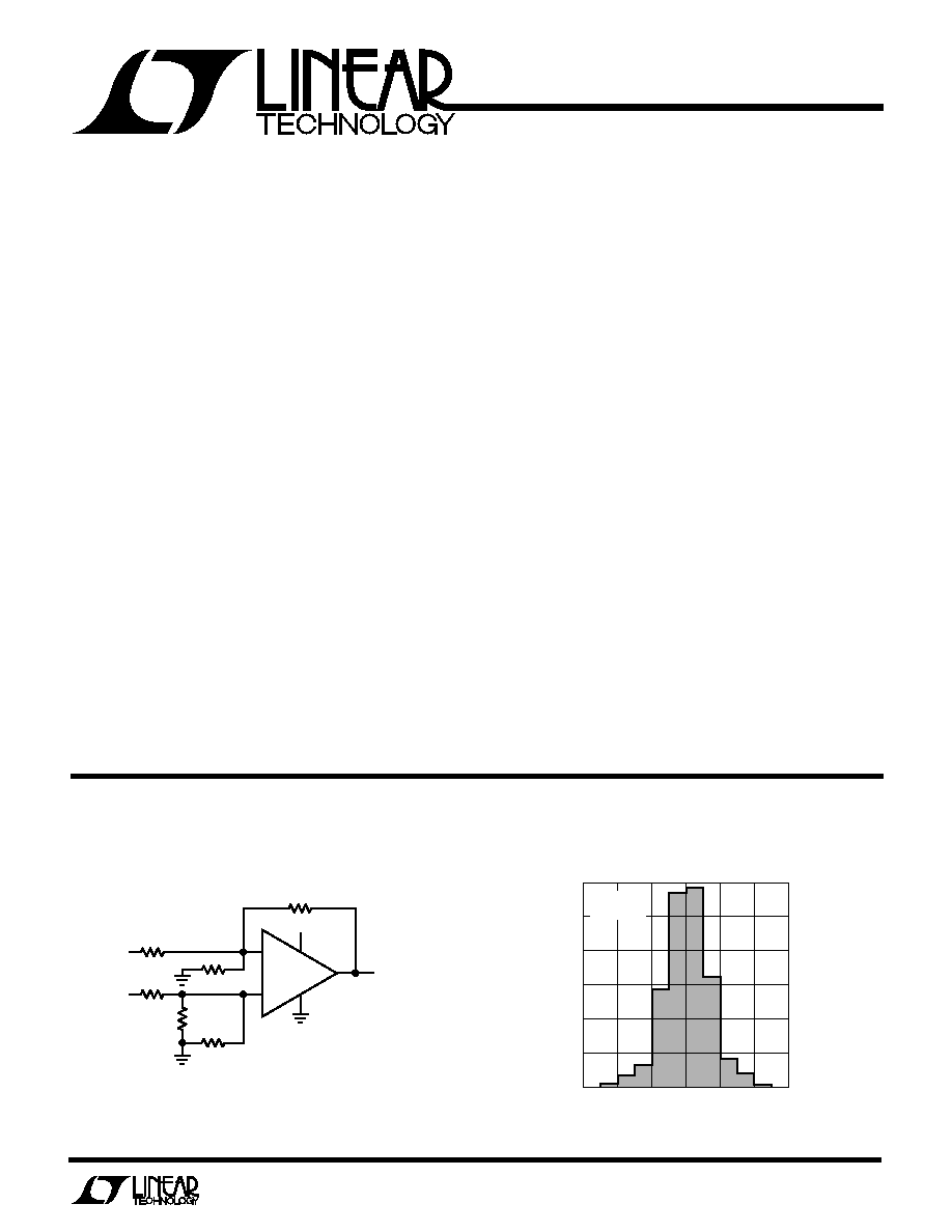
+90V, ≠3V Common-Mode Range
Difference Amplifier (A
V
= 1)
Distribution of Input Offset Voltage
(In Plastic DIP, N8 Package)
INPUT OFFSET VOLTAGE (
µ
V)
≠300
0
PERCENT OF UNITS
5
10
15
20
30
≠200
≠100
0
100
LT1413 ∑ TA01
200
300
25
V
S
= 5V, 0V
T
A
= 25
∞
C
LT1413 ∑ TA03
10M
≠
+
≠
+
10M
1M
10M
1M
1/2 LT1413
9V
10M
OUTPUT
20mV TO 8V
1
8
4
3
2
INPUT
1.5mV
125
µ
V)
11M
80kHz
OUTPUT OFFSET =
(INPUT REFERRED =
INPUT RESISTANCE =
BANDWIDTH =
(THE 0.1nA TYPICAL OFFSET CURRENT
PERMITS THE USE OF 1M
RESISTORS)
U
A
O
PPLICATI
TYPICAL

2
LT1413
LT1413ACN8
SYMBOL
PARAMETER
CONDITIONS (Note 1)
MIN
TYP
MAX
MIN
TYP
MAX
UNITS
V
OS
Input Offset Voltage
LT1413N8
50
150
60
280
µ
V
LT1413S8
80
380
µ
V
V
OS
Long-Term Input Offset
0.4
0.5
µ
V/Mo
Time
Voltage Stability
I
OS
Input Offset Current
0.1
0.7
0.1
0.8
nA
I
B
Input Bias Current
9
15
9
18
nA
e
n
Input Noise Voltage
0.1Hz to 10Hz (Note 2)
0.55
1.1
0.55
µ
V
P-P
Input Noise Voltage Density
f
O
= 10Hz (Note 2)
24
38
24
nV/
Hz
f
O
= 1000Hz (Note 2)
23
30
23
nV/
Hz
i
n
Input Noise Current
0.1Hz to 10Hz
2.8
2.8
pA
P-P
Input Noise Current Density
f
O
= 10Hz
0.07
0.07
pA/
Hz
f
O
= 1000Hz
0.02
0.02
pA/
Hz
Input Resistance
(Note 3)
Differential Mode
300
500
250
500
M
Common Mode
3
3
G
Input Voltage Range
3.65
3.8
3.65
3.8
V
0
≠ 0.3
0
≠ 0.3
V
CMRR
Common-Mode Rejection Ratio
V
CM
= 0V to 3.65V
90
101
88
101
dB
PSRR
Power Supply Rejection Ratio
V
S
= 3.2V to 12V
102
118
100
118
dB
A
VOL
Large-Signal Voltage Gain
V
O
= 0.05V to 4V, No Load
400
1400
350
1400
V/mV
V
O
= 0.05V to 3.5V, R
L
= 2k
300
1000
250
1000
V/mV
1
2
3
4
8
7
6
5
TOP VIEW
≠IN A
OUT A
V
+
OUT B
+IN A
V
≠
+IN B
≠IN B
S8 PACKAGE
8-LEAD PLASTIC SOIC
A
B
NOTE: THIS PIN CONFIGURATION DIFFERS FROM
THE 8-LEAD DIP PIN LOCATIONS. INSTEAD, IT
FOLLOWS THE INDUSTRY STANDARD LT1013DS8
SO PACKAGE CONFIGURATION.
A
U
G
W
A
W
U
W
A
R
BSOLUTE
XI
TI
S
Supply Voltage .....................................................
±
22V
Differential Input Voltage ......................................
±
30V
Input Voltage ..................................................................
Equal to Positive Supply Voltage
5V Below Negative Supply Voltage
Output Short-Circuit Duration ......................... Indefinite
Operating Temperature Range ............... ≠ 40
∞
C to 85
∞
C
Storage Temperature Range ................ ≠ 65
∞
C to 150
∞
C
Lead Temperature (Soldering, 10 sec) ................. 300
∞
C
Note: When the input voltage exceeds the maximum ratings, the input current should be limited
to 10mA.
W
U
U
PACKAGE/ORDER I FOR ATIO
LT1413ACN8
LT1413CN8
ORDER PART
NUMBER
ORDER PART
NUMBER
LT1413S8
T
JMAX
= 105
∞
C,
JA
= 200
∞
C/ W
S8 PART MARKING
1413
T
JMAX
= 100
∞
C,
JA
= 130
∞
C/ W
1
2
3
4
8
7
6
5
TOP VIEW
OUT A
≠IN A
+IN A
V
≠
V
+
OUT B
≠IN B
+IN B
N8 PACKAGE
8-LEAD PLASTIC DIP
A
B
ELECTRICAL C
C
HARA TERISTICS
LT1413CN8/S8
V
S
= 5V, 0V, V
CM
= 0.1V, V
O
= 1.4V, T
A
= 25
∞
C, unless otherwise noted.

3
LT1413
LT1413ACN8
LT1413CN8/S8
SYMBOL
PARAMETER
CONDITIONS
MIN
TYP
MAX
MIN
TYP
MAX
UNITS
Maximum Output Voltage Swing
Output Low, No Load
15
25
15
25
mV
Output Low, 600
to GND
5
10
5
10
mV
Output Low, I
SINK
= 1mA
220
350
220
350
mV
Output High, No Load
4.1
4.4
4.1
4.4
V
Output High, 600
to GND
3.4
4.0
3.4
4.0
V
SR
Slew Rate
A
V
= 1
0.2
0.3
0.2
0.3
V/
µ
s
GBW
Gain-Bandwidth Product
f
O
100kHz (Note 4)
600
950
600
950
kHz
I
S
Supply Current per Amplifier
330
450
330
480
µ
A
Channel Separation
V
IN
= 3V, R
L
= 2k (Note 5)
125
140
123
140
dB
Minimum Supply Voltage
(Note 6)
2.85
3.0
2.85
3.0
V
ELECTRICAL C
C
HARA TERISTICS
LT1413ACN8
LT1413CN8/S8
SYMBOL
PARAMETER
CONDITIONS (Note 1)
MIN
TYP
MAX
MIN
TYP
MAX
UNITS
V
OS
Input Offset Voltage
LT1413N8
q
70
300
85
470
µ
V
LT1413S8
q
110
570
µ
V
V
OS
/
T
Input Offset Voltage Drift
q
0.3
2.2
0.4
2.8
µ
V/
∞
C
I
OS
Input Offset Current
q
0.2
1.4
0.2
1.7
nA
I
B
Input Bias Current
q
11
25
11
30
nA
CMRR
Common-Mode Rejection Ratio
V
CM
= 0V to 3.4V
q
85
99
82
99
dB
PSRR
Power Supply Rejection Ratio
V
S
= 3.9V to 12V
q
98
116
94
116
dB
A
VOL
Large-Signal Voltage Gain
V
O
= 0.08V to 3.8V, No Load
q
220
1000
220
1000
V/mV
V
O
= 0.08V to 3.0V, R
L
= 2k
q
150
700
150
700
V/mV
Maximum Output Voltage Swing
Output Low, No Load
q
20
38
20
38
mV
Output Low, I
SINK
= 1mA
q
300
480
300
480
mV
Output High, No Load
q
3.9
4.2
3.9
4.2
V
Output High, 600
to GND
q
3.1
3.8
3.0
3.8
V
I
S
Supply Current per Amplifier
q
360
550
360
580
µ
A
V
S
= 5V, 0V, V
CM
= 0.1V, V
O
= 1.4V, 0
∞
C
T
A
70
∞
C, unless otherwise noted.
LT1413ACN8
LT1413CN8/S8
SYMBOL
PARAMETER
CONDITIONS (Note 1)
MIN
TYP
MAX
MIN
TYP
MAX
UNITS
V
OS
Input Offset Voltage
LT1413N8
q
65
240
80
390
µ
V
LT1413S8
q
100
490
µ
V
V
OS
/
T
Input Offset Voltage Drift
(Note 5)
q
0.3
2.0
0.4
2.5
µ
V/
∞
C
I
OS
Input Offset Current
q
0.1
1.0
0.1
1.2
nA
I
B
Input Bias Current
q
10
20
10
23
nA
CMRR
Common-Mode Rejection Ratio
V
CM
= 0V to 3.6V
q
88
100
85
100
dB
PSRR
Power Supply Rejection Ratio
V
S
= 3.45V to 12V
q
100
117
97
117
dB
A
VOL
Large-Signal Voltage Gain
V
O
= 0.07V to 3.9V, No Load
q
300
1100
300
1100
V/mV
V
O
= 0.07V to 3.2V, R
L
= 2k
q
200
800
200
800
V/mV
Maximum Output Voltage Swing
Output Low, No Load
q
18
32
18
32
mV
Output Low, I
SINK
= 1mA
q
270
430
270
430
mV
Output High, No Load
q
4.0
4.3
4.0
4.3
V
Output High, 600
to GND
q
3.3
3.9
3.2
3.9
V
I
S
Supply Current per Amplifier
q
350
500
350
530
µ
A
V
S
= 5V, 0V, V
CM
= 0.1V, V
O
= 1.4V, T
A
= 25
∞
C, unless otherwise noted.
V
S
= 5V, 0V, V
CM
= 0.1V, V
O
= 1.4V, ≠ 40
∞
C
T
A
85
∞
C (Note 7)
4
LT1413
LT1413ACN8
LT1413CN8/S8
SYMBOL
PARAMETER
CONDITIONS (Note 1)
MIN
TYP
MAX
MIN
TYP
MAX
UNITS
V
OS
Input Offset Voltage
LT1413N8
75
280
90
480
µ
V
LT1413S8
110
580
µ
V
I
OS
Input Offset Current
0.1
0.7
0.1
0.8
nA
I
B
Input Bias Current
8
15
8
18
nA
Input Voltage Range
13.5
13.8
13.5
13.8
V
≠ 15.0
≠ 15.3
≠ 15.0
≠ 15.3
V
CMRR
Common-Mode Rejection Ratio
V
CM
= 13.5V, ≠ 15V
100
117
97
114
dB
PSRR
Power Supply Rejection Ratio
V
S
=
±
2V to
±
18V
103
120
100
117
dB
A
VOL
Large-Signal Voltage Gain
V
O
=
±
10V, R
L
= 2k
1500
5000
1200
4000
V/mV
V
OUT
Maximum Output Voltage Swing
R
L
= 2k
±
13
±
14
±
12.5
±
14
V
SR
Slew Rate
0.2
0.4
0.2
0.4
V/
µ
s
I
S
Supply Current per Amplifier
350
500
350
550
µ
A
ELECTRICAL C
C
HARA TERISTICS
LT1413ACN8
LT1413CN8/S8
SYMBOL
PARAMETER
CONDITIONS (Note 1)
MIN
TYP
MAX
MIN
TYP
MAX
UNITS
V
OS
Input Offset Voltage
LT1413N8
q
95
390
110
620
µ
V
LT1413S8
q
130
720
µ
V
V
OS
/
T
Input Offset Voltage Drift
(Note 5)
q
0.4
2.5
0.5
3.0
µ
V/
∞
C
I
OS
Input Offset Current
q
0.1
1.0
0.1
1.2
nA
I
B
Input Bias Current
q
9
20
9
23
nA
A
VOL
Large-Signal Voltage Gain
V
O
=
±
10V, R
L
= 2k
q
1000
4000
700
3000
V/mV
CMRR
Common-Mode Rejection Ratio
V
CM
= 13V, ≠ 15V
q
98
116
94
113
dB
PSRR
Power Supply Rejection Ratio
V
S
=
±
2V to
±
18V
q
101
119
97
116
dB
Maximum Output Voltage Swing
R
L
= 2k
q
±
12.5
±
13.9
±
12.0
±
13.9
V
I
S
Supply Current per Amplifier
q
360
550
360
600
µ
A
LT1413ACN8
LT1413CN8/S8
SYMBOL
PARAMETER
CONDITIONS (Note 1)
MIN
TYP
MAX
MIN
TYP
MAX
UNITS
V
OS
Input Offset Voltage
LT1413N8
q
100
460
120
700
µ
V
LT1413S8
q
140
800
µ
V
V
OS
/
T
Input Offset Voltage Drift
q
0.4
2.8
0.5
3.3
µ
V/
∞
C
I
OS
Input Offset Current
q
0.2
1.4
0.2
1.7
nA
I
B
Input Bias Current
q
10
25
10
30
nA
A
VOL
Large-Signal Voltage Gain
V
O
=
±
10V, R
L
= 2k
q
800
3000
500
2400
V/mV
CMRR
Common-Mode Rejection Ratio
V
CM
= 13V, ≠ 15V
q
97
115
92
112
dB
PSRR
Power Supply Rejection Ratio
V
S
±
2V to
±
18V
q
100
118
95
115
dB
Maximum Output Voltage Swing
R
L
= 2k
q
±
12.2
±
13.8
±
11.8
±
13.8
V
I
S
Supply Current per Amplifier
q
370
580
370
630
µ
A
The
q
denotes specifications which apply over the full operating
temperature range.
Note 1: Typical parameters are defined as the 60% yield of parameter
distributions of individual amplifiers; i.e., out of 100 LT1413s typically 120
op amps will be better than the indicated specification.
Note 2: This parameter is tested on a sample basis only. All noise
parameters are tested with V
S
=
±
2.5V, V
O
= 0V.
Note 3: This parameter is guaranteed by design and is not tested.
V
S
=
±
15V, T
A
= 25
∞
C, unless otherwise noted.
Note 4: Gain-Bandwidth Product is not tested. It is inferred from the slew
rate measurement.
Note 5: This parameter is not 100% tested.
Note 6: At the minimum supply voltage, the offset voltage changes less
than 200
µ
V compared to its value at 5V, 0V.
Note 7: The LT1413 is not tested and is not quality-assurance sampled at
≠ 40
∞
C and at 85
∞
C. These specifications are guaranteed by design,
correlation and/or inference from 0
∞
C, 25
∞
C and/or 70
∞
C tests.
V
S
=
±
15V, ≠ 40
∞
C
T
A
85
∞
C (Note 7)
V
S
=
±
15V, 0
∞
C
T
A
70
∞
C, unless otherwise noted.

5
LT1413
C
C
HARA TERISTICS
U
W
A
TYPICAL PERFOR
CE
INPUT OFFSET VOLTAGE (
µ
V)
≠400
0
PERCENT OF UNITS
5
10
15
20
≠200
0
200
400
LT1413 ∑ TA02
25
30
≠300
≠100
100
300
V
S
= 5V, 0V
T
A
= 25
∞
C
Distribution of Input Offset Voltage
(In S8 Package)
TEMPERATURE (
∞
C)
SUPPLY CURRENT PER AMPLIFIER (
µ
A)
350
400
25
100
LT1413 ∑ TA04
300
0
≠25
≠ 50
50
75
V
S
= 5V, 0V
V
S
=
±
15V
Supply Current vs Temperature
TEMPERATURE (
∞
C)
0.01
SATURATION VOLTAGE (V)
0.1
10
0
100
LT1413 ∑ TA05
50
1
≠25
25
75
≠ 50
I
SINK
= 10mA
I
SINK
= 5mA
I
SINK
= 1mA
I
SINK
= 100
µ
A
I
SINK
= 10
µ
A
I
SINK
= 0
V
+
= 5V TO 30V
V
≠
= 0V
Input Offset Current vs Temperature
TEMPERATURE (
∞
C)
INPUT BIAS CURRENT (nA)
≠ 9
≠11
40
100
LT1413 ∑ TA07
≠7
0
≠20
≠ 40
60
80
≠10
≠ 8
20
V
S
=
±
15V
5V, 0V
0.1V
V
S
=
V
CM
=
Input Bias Current vs Temperature
Output Saturation vs Sink
Current vs Temperature
INPUT BIAS CURRENT (nA)
COMMON-MODE VOLTAGE (V)
0
15
≠10
≠16
LT1413 ∑ TA08
≠15
≠ 4
≠2
0
≠12 ≠14
10
≠10
≠ 6
≠ 5
5
≠ 8
COMMON-MODE VOLTAGE (V)
2
5
≠1
4
0
1
3
V
S
= 5V, 0V
T
A
= 25
∞
C
V
S
=
±
15V
Input Bias Current vs
Common-Mode Voltage
0.1Hz to 10Hz Noise
FREQUENCY (Hz)
1
10
VOLTAGE NOISE DENSITY (nV/
Hz)
CURRENT NOISE DENSITY (fA
/
Hz)
30
1000
10
1k
LT1413 ∑ TA10
100
300
100
T
A
= 25
∞
C
V
S
=
±
2V TO
±
18V
CURRENT NOISE
VOLTAGE NOISE
1/f CORNER 2Hz
Noise Spectrum
Minimum Supply Voltage
POSITIVE SUPPLY VOLTAGE (V)
CHANGE IN OFFSET VOLTAGE (
µ
V)
100
200
5
LT1413 ∑ TA11
0
3
2
4
T
A
= ≠ 40
∞
C
T
A
= 0
∞
C
T
A
= 25
∞
C
T
A
= 85
∞
C
NONFUNCTIONAL
V
≠
= 0V
TEMPERATURE (
∞
C)
INPUT OFFSET CURRENT (pA)
150
250
40
100
LT1413 ∑ TA06
50
0
≠20
≠ 40
60
80
200
100
0
20
V
S
=
±
15V
5V, 0V
0.1V
V
S
=
V
CM
=
TIME (SECONDS)
NOISE VOLTAGE (200nV/DIV)
10
LT1413 ∑ TA09
4
2
0
6
8
T
A
= 25
∞
C
V
S
=
±
2V TO
±
18V