Äîêóìåíòàöèÿ è îïèñàíèÿ www.docs.chipfind.ru
1
LT1460-10
Micropower Precision
Series Reference
FEATURES
DESCRIPTIO
N
U
s
High Accuracy: 0.075% Max
s
Low Drift: 10ppm/
°
C Max
s
Industrial Temperature Range SO-8 Package
s
Low Supply Current: 270
µ
A Max
s
Minimum Output Current: 20mA
s
No Output Capacitor Required
s
Reverse Battery Protection
s
Minimum Input/Output Differential: 0.9V
s
Available in Small MSOP Package
The LT
®
1460-10 is a micropower bandgap reference that
combines very high accuracy and low drift with low power
dissipation and small package size. This series reference
uses curvature compensation to obtain a low temperature
coefficient and trimmed precision thin-film resistors to
achieve high output accuracy. The reference will supply up to
20mA, making it ideal for precision regulator applications, yet
it is almost totally immune to input voltage variations.
This series reference provides supply current and power
dissipation advantages over shunt references that must idle
the entire load current to operate. Additionally, the LT1460-10
does not require an output capacitor, but it is stable with
capacitive loads. This feature is important in critical applica-
tions where PC board space is a premium or fast settling is
demanded. Reverse battery protection keeps the reference
from conducting current and being damaged.
The LT1460-10 is available in the 8-lead MSOP, SO, PDIP
and the 3-lead TO-92 packages. It is also available in the
SOT-23 package; see separate data sheet LT1460S3-10
(SOT-23).
APPLICATIO
N
S
U
s
Handheld Instruments
s
Precision Regulators
s
A/D and D/A Converters
s
Power Supplies
s
Hard Disk Drives
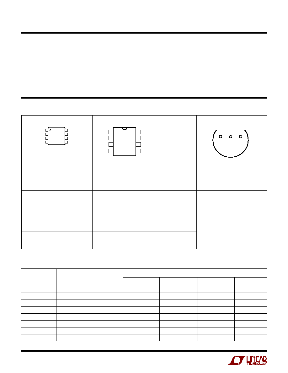
Typical Distribution of Output Voltage
S8 Package
, LTC and LT are registered trademarks of Linear Technology Corporation.
TYPICAL APPLICATIO
N
U
OUTPUT VOLTAGE ERROR (%)
0.10
UNITS (%)
0.06
0.02 0
1460-10 TA02
0.06
0.02
20
18
16
14
12
10
8
6
4
2
0
0.10
1400 PARTS
FROM 2 RUNS
Basic Connection
LT1460-10
GND
IN
OUT
1460-10 TA01
C1
0.1
µ
F
10V
10.9V
TO 20V
2
LT1460-10
ABSOLUTE
M
AXI
M
U
M
RATINGS
W
W
W
U
Input Voltage ........................................................... 30V
Reverse Voltage .................................................... 15V
Output Short-Circuit Duration, T
A
= 25
°
C ............. 5 sec
Specified Temperature Range
Commercial ............................................ 0
°
C to 70
°
C
Industrial ........................................... 40
°
C to 85
°
C
Storage Temperature Range (Note 1) ... 65
°
C to 150
°
C
Lead Temperature (Soldering, 10 sec) .................. 300
°
C
Available Options
TEMPERATURE
PACKAGE TYPE
ACCURACY
COEFFICIENT
TEMPERATURE
(%)
(ppm/
°
C)
N8
S8
MS8
Z
0
°
C to 70
°
C
0.075
10
LT1460ACN8-10
LT1460ACS8-10
40
°
C to 85
°
C
0.10
10
LT1460BIN8-10
LT1460BIS8-10
0
°
C to 70
°
C
0.10
15
LT1460CCMS8-10
0
°
C to 70
°
C
0.10
20
LT1460DCN8-10
LT1460DCS8-10
40
°
C to 85
°
C
0.125
20
LT1460EIN8-10
LT1460EIS8-10
0
°
C to 70
°
C
0.15
25
LT1460FCMS8-10
0
°
C to 70
°
C
0.25
25
LT1460GCZ-10
40
°
C to 85
°
C
0.25
25
LT1460GIZ-10
PACKAGE/ORDER I
N
FOR
M
ATIO
N
W
U
U
1
2
3
4
NC*
V
IN
NC*
GND
8
7
6
5
NC*
NC*
V
OUT
NC*
TOP VIEW
MS8 PACKAGE
8-LEAD PLASTIC MSOP
*CONNECTED INTERNALLY.
DO NOT CONNECT EXTERNAL
CIRCUITRY TO THESE PINS
MS8 PART MARKING
ORDER PART NUMBER
ORDER PART NUMBER
ORDER PART NUMBER
S8 PART MARKING
1460A1
460BI1
LTAH
LTAJ
1460D1
460EI1
T
JMAX
= 150
°
C,
JA
= 250
°
C/ W
1
2
3
4
8
7
6
5
TOP VIEW
NC*
V
IN
NC*
GND
NC*
NC*
V
OUT
NC*
N8 PACKAGE
8-LEAD PDIP
S8 PACKAGE
8-LEAD PLASTIC SO
*CONNECTED INTERNALLY.
DO NOT CONNECT
EXTERNAL CIRCUITRY
TO THESE PINS
T
JMAX
= 150
°
C,
JA
= 130
°
C/ W (N8)
T
JMAX
= 150
°
C,
JA
= 190
°
C/ W (S8)
1
2
3
BOTTOM VIEW
V
IN
V
OUT
GND
Z PACKAGE
3-LEAD TO-92 PLASTIC
T
JMAX
= 150
°
C,
JA
= 160
°
C/ W
LT1460CCMS8-10
LT1460FCMS8-10
LT1460ACS8-10
LT1460BIS8-10
LT1460DCS8-10
LT1460EIS8-10
LT1460ACN8-10
LT1460BIN8-10
LT1460DCN8-10
LT1460EIN8-10
LT1460GCZ-10
LT1460GIZ-10
Consult factory for Military grade parts.
3
LT1460-10
PARAMETER
CONDITIONS
MIN
TYP
MAX
UNITS
Output Voltage (Note 2)
LT1460ACN8, ACS8
9.9925
10.000 10.0075
V
0.075
0.075
%
LT1460BIN8, BIS8, CCMS8, DCN8, DCS8
9.990
10.000
10.010
V
0.10
0.10
%
LT1460EIN8, EIS8
9.9875
10.000
10.0125
V
0.125
0.125
%
LT1460FCMS8
9.985
10.000
10.015
V
0.15
0.15
%
LT1460GCZ, GIZ
9.975
10.000
10.025
V
0.25
0.25
%
Output Voltage Temperature Coefficient (Note 3)
T
MIN
T
J
T
MAX
LT1460ACN8, ACS8, BIN8, BIS8
q
5
10
ppm/
°
C
LT1460CCMS8
q
7
15
ppm/
°
C
LT1460DCN8, DCS8, EIN8, EIS8
q
10
20
ppm/
°
C
LT1460FCMS8, GCZ, GIZ
q
12
25
ppm/
°
C
Line Regulation
10.9V
V
IN
12.5V
30
60
ppm/V
q
80
ppm/V
12.5V
V
IN
20V
10
25
ppm/V
q
35
ppm/V
Load Regulation Sourcing (Note 4)
I
OUT
= 100
µ
A
1500
2800
ppm/mA
q
3500
ppm/mA
I
OUT
= 10mA
80
135
ppm/mA
q
180
ppm/mA
I
OUT
= 20mA
70
100
ppm/mA
0
°
C to 70
°
C
q
140
ppm/mA
Thermal Regulation (Note 5)
P = 200mW
0.5
2.5
ppm/mW
Dropout Voltage (Note 6)
V
IN
V
OUT
,
V
OUT
0.1%, I
OUT
= 0
q
0.9
V
V
IN
V
OUT
,
V
OUT
0.1%, I
OUT
= 10mA
1.3
V
q
1.4
V
Output Current
Short V
OUT
to GND
40
mA
Reverse Leakage
V
IN
= 15V
q
0.5
10
µ
A
Supply Current
190
270
µ
A
q
360
µ
A
Output Voltage Noise (Note 7)
0.1Hz
f
10Hz
40
µ
V
P-P
10Hz
f
1kHz
35
µ
V
RMS
Long-Term Stability of Output Voltage, S8 Pkg (Note 8)
40
ppm/
kHr
Hysteresis (Note 9)
T = 40
°
C to 85
°
C
160
ppm
T = 0
°
C to 70
°
C
25
ppm
The
q
denotes specifications which apply over the specified temperature
range.
Note 1: If the part is stored outside of the specified temperature range, the
output may shift due to hysteresis.
Note 2: ESD (Electrostatic Discharge) sensitive device. Extensive use of
ESD protection devices are used internal to the LT1460-10, however, high
electrostatic discharge can damage or degrade the device. Use proper ESD
handling precautions.
Note 3: Temperature coefficient is measured by dividing the change in
output voltage by the specified temperature range. Incremental slope is
also measured at 25
°
C.
Note 4: Load regulation is measured on a pulse basis from no load to the
specified load current. Output changes due to die temperature change
must be taken into account separately.
Note 5: Thermal regulation is caused by die temperature gradients created
by load current or input voltage changes. This effect must be added to
normal line or load regulation. This parameter is not 100% tested.
ELECTRICAL CHARACTERISTICS
V
IN
= 12.5V, I
OUT
= 0, T
A
= 25
°
C unless otherwise specified.
4
LT1460-10
ELECTRICAL CHARACTERISTICS
Note 6: Excludes load regulation errors.
Note 7: Peak-to-peak noise is measured with a single highpass filter at
0.1Hz and a 2-pole lowpass filter at 10Hz. The unit is enclosed in a still-air
environment to eliminate thermocouple effects on the leads. The test time
is 10 sec. RMS noise is measured with a single highpass filter at 10Hz and
a 2-pole lowpass filter at 1kHz. The resulting output is full wave rectified
and then integrated for a fixed period, making the final reading an average
as opposed to RMS. A correction factor of 1.1 is used to convert from
average to RMS and a second correction of 0.88 is used to correct for the
nonideal bandpass of the filters.
Note 8: Long-term stability typically has a logarithmic characteristic and
therefore, changes after 1000 hours tend to be much smaller than before
that time. Total drift in the second thousand hours is normally less than
one third that of the first thousand hours with a continuing trend toward
reduced drift with time. Significant improvement in long-term drift can be
realized by preconditioning the IC with a 100 hour to 200 hour, 125
°
C
burn-in. Long-term stability will also be affected by differential stresses
between the IC and the board material created during board assembly. See
PC Board Layout in the Applications Information section.
Note 9: Hysteresis in output voltage is created by package stress that
differs depending on whether the IC was previously at a higher or lower
temperature. Output voltage is always measured at 25
°
C, but the IC is
cycled to 85
°
C or 40
°
C before successive measurements. Hysteresis is
roughly proportional to the square of the temperature change. Hysteresis
is not normally a problem for operational temperature excursions where
the instrument might be stored at high or low temperature.
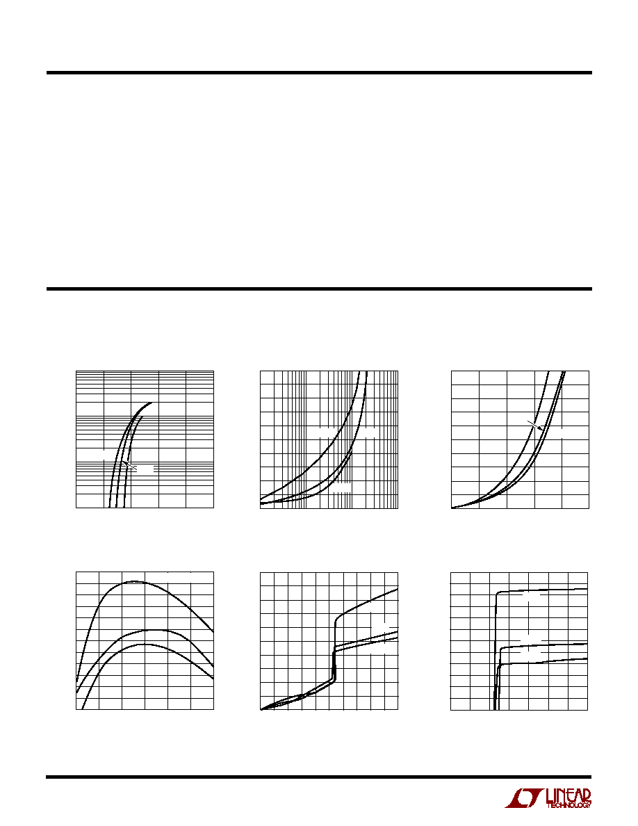
TYPICAL PERFOR
M
A
N
CE CHARACTERISTICS
U
W
OUTPUT CURRENT (mA)
0
OUTPUT VOLTAGE CHANGE (mV)
60
80
100
4
1460-10 G03
40
20
50
70
90
30
10
0
1
2
3
5
55
°
C
125
°
C
25
°
C
Load Regulation, Sinking
Line Regulation
TEMPERATURE (
°
C)
50
9.982
OUTPUT VOLTAGE (V)
9.986
9.990
9.994
9.998
10.006
25
0
25
50
1460-10 G04
75
100
10.002
3 TYPICAL PARTS
Output Voltage Temperature Drift
INPUT/OUTPUT VOLTAGE (V)
0
0.1
OUTPUT CURRENT (mA)
100
0.5
1.0
1.5
2.0
2.5
1460-10 G01
10
1
55
°
C
125
°
C
25
°
C
Minimum Input/Output
Voltage Differential
INPUT VOLTAGE (V)
6
9.980
OUTPUT VOLTAGE (V)
9.984
9.988
9.992
9.996
10.004
10
14
18
1460-10 G06
8
12
16
20
10.000
55
°
C
125
°
C
25
°
C
Supply Current vs Input Voltage
INPUT VOLTAGE (V)
0
SUPPLY CURRENT (
µ
A)
240
320
400
16
1460-10 G05
160
80
200
280
360
120
40
0
4
8
12
2
18
6
10
14
20
55
°
C
125
°
C
25
°
C
OUTPUT CURRENT (mA)
0.1
4
OUTPUT VOLTAGE CHANGE (mV)
5
6
7
8
1
10
100
1460-10 G02
3
2
1
0
9
10
55
°
C
25
°
C
125
°
C
Load Regulation, Sourcing
5
LT1460-10
TYPICAL PERFOR
M
A
N
CE CHARACTERISTICS
U
W
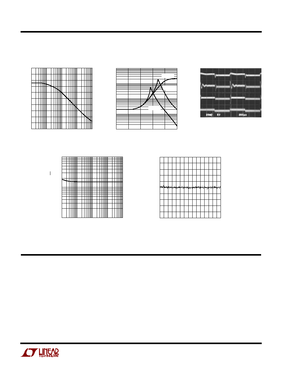
Power Supply Rejection Ratio
vs Frequency
Transient Responses
10
1
0.1
0
200
µ
s/DIV
LOAD CAPACITANCE (
µ
F)
I
OUT
= 10mA
1460-10 G09
Output Impedance vs Frequency
FREQUENCY (kHz)
1
OUTPUT IMPEDANCE (
)
10
100
1000
0.01
1
10
100
0.1
0.1
1000
1460-10 G08
C
L
= 0
µ
F
C
L
= 1
µ
F
C
L
= 0.1
µ
F
Output Voltage Noise Spectrum
FREQUENCY (kHz)
0.01
0.1
1
10
1
10
0.1
100
1460-10 G10
NOISE VOLTAGE (
µ
V/
Hz)
Output Noise 0.1Hz to 10Hz
TIME (SEC)
0
OUTPUT NOISE (50
µ
V/DIV)
8
1460-10 G11
2
4
6
10
12
14
APPLICATIO
N
S I
N
FOR
M
ATIO
N
W
U
U
U
Precision Regulator
The LT1460-10 is ideal as a precision regulator, and since
it operates in series mode it does not require a current
setting resistor. The reference can supply up to 20mA of
load current with good transient response. Load regula-
tion at 20mA output is typically 70ppm/mA meaning the
output changes only 14mV.
Capacitive Loads
The LT1460-10 is designed to be stable with capacitive
loads. With no capacitive load, the reference is ideal for
fast settling or applications where PC board space is a
premium. The test circuit shown in Figure 1 is used to
measure the response time for various load currents and
load capacitors. The 1V step from 10V to 9V produces a
INPUT FREQUENCY (kHz)
20
POWER SUPPLY REJECTION RATIO (dB)
40
60
50
80
100
10
30
70
90
0.1
10
100
1000
1460-10 G07
0
1