1460S3 Layout
1
LT1460S3 (SOT-23)
Family of Micropower
Series References
in SOT-23
3-Lead SOT-23 Package
Low Drift: 20ppm/
°
C Max
High Accuracy: 0.2% Max
Low Supply Current
20mA Output Current Guaranteed
No Output Capacitor Required
Reverse-Battery Protection
Low PC Board Solder Stress: 0.02% Typ
Voltage Options: 2.5V, 3V, 3.3V, 5V and 10V
The LT1460 is Also Available in SO-8, 8-Lead MSOP,
8-Lead PDIP and TO-92 Packages.
Operating Temperature Range: 40
°
C to 85
°
C
The LT
®
1460S3 is a family of SOT-23 micropower series
references that combine high accuracy and low drift with low
power dissipation and small package size. These series
references use curvature compensation to obtain low tem-
perature coefficient, and laser trimmed precision thin-film
resistors to achieve high output accuracy. Furthermore,
output shift due to PC board soldering stress has been
dramatically reduced. These references will supply up to
20mA, making them ideal for precision regulator applica-
tions, yet they are almost totally immune to input voltage
variations.
These series references provide supply current and power
dissipation advantages over shunt references that must idle
the entire load current to operate. Additionally, the
LT1460S3 does not require an output compensation capaci-
tor. This feature is important in applications where PC board
space is a premium or fast settling is demanded. Reverse-
battery protection keeps these references from conducting
reverse current.
Handheld Instruments
Precision Regulators
A/D and D/A Converters
Power Supplies
Hard Disk Drives
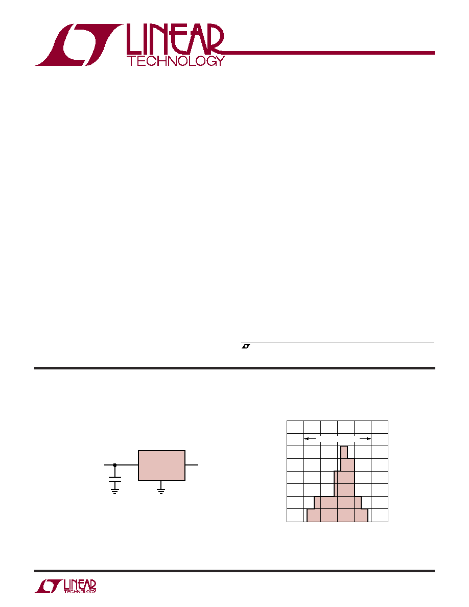
Basic Connection
, LTC and LT are registered trademarks of Linear Technology Corporation.
Typical Distribution of SOT-23 LT1460HC
V
OUT
After IR Reflow Solder
FEATURES
DESCRIPTIO
U
APPLICATIO S
U
TYPICAL APPLICATIO
U
LT1460S3
GND
IN
OUT
V
OUT
+ 0.9V
V
IN
20V
1460S3 TA01
C1
0.1
µ
F
V
OUT
OUTPUT VOLTAGE ERROR (%)
0.3
DISTRIBUTION (%)
12
16
20
0
0.2
1460S3 TA02
8
4
0
0.2
0.1
0.1
24
28
32
0.3
LT1460HC LIMITS
2
LT1460S3 (SOT-23)
ABSOLUTE
M
AXI
M
U
M
RATINGS
W
W
W
U
PACKAGE/ORDER I
N
FOR
M
ATIO
N
W
U
U
Input Voltage ........................................................... 30V
Reverse Voltage .................................................... 15V
Output Short-Circuit Duration, T
A
= 25
°
C .............. 5 sec
Specified Temperature Range ..................... 0
°
C to 70
°
C
ORDER PART
NUMBER
S3
PART MARKING
Product may be identified with either part marking. *The temperature grades and parametric grades are identified by a label on the shipping container.
Consult factory for Industrial and Military grade parts.
T
JMAX
= 125
°
C,
JA
= 325
°
C/ W
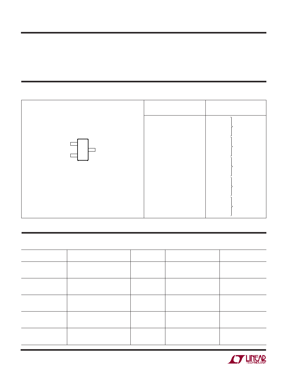
3 GND
IN 1
TOP VIEW
S3 PACKAGE
3-LEAD PLASTIC SOT-23
OUT 2
LTAC
LTAD
LTAE
LTAN
LTAP
LTAQ
LTAR
LTAS
LTAT
LTAK
LTAL
LTAM
LTAU
LTAV
LTAW
Operating Temperature Range
(Note 2) ............................................. 40
°
C to 85
°
C
Storage Temperature Range (Note 3) ... 65
°
C to 150
°
C
Lead Temperature (Soldering, 10 sec).................. 300
°
C
(Note 1)
LT1460HCS3-2.5
LT1460JCS3-2.5
LT1460KCS3-2.5
LT1460HCS3-3
LT1460JCS3-3
LT1460KCS3-3
LT1460HCS3-3.3
LT1460JCS3-3.3
LT1460KCS3-3.3
LT1460HCS3-5
LT1460JCS3-5
LT1460KCS3-5
LT1460HCS3-10
LT1460JCS3-10
LT1460KCS3-10
AVAILABLE OPTIO S
U
OUTPUT VOLTAGE
SPECIFIED TEMPERATURE
ACCURACY
TEMPERATURE
PART ORDER
(V)
RANGE
(%)
COEFFICIENT (ppm/
°
C)
NUMBER
2.5
0
°
C to 70
°
C
0.2
20
LT1460HCS3-2.5
2.5
0
°
C to 70
°
C
0.4
20
LT1460JCS3-2.5
2.5
0
°
C to 70
°
C
0.5
50
LT1460KCS3-2.5
3
0
°
C to 70
°
C
0.2
20
LT1460HCS3-3
3
0
°
C to 70
°
C
0.4
20
LT1460JCS3-3
3
0
°
C to 70
°
C
0.5
50
LT1460KCS3-3
3.3
0
°
C to 70
°
C
0.2
20
LT1460HCS3-3.3
3.3
0
°
C to 70
°
C
0.4
20
LT1460JCS3-3.3
3.3
0
°
C to 70
°
C
0.5
50
LT1460KCS3-3.3
5
0
°
C to 70
°
C
0.2
20
LT1460HCS3-5
5
0
°
C to 70
°
C
0.4
20
LT1460JCS3-5
5
0
°
C to 70
°
C
0.5
50
LT1460KCS3-5
10
0
°
C to 70
°
C
0.2
20
LT1460HCS3-10
10
0
°
C to 70
°
C
0.4
20
LT1460JCS3-10
10
0
°
C to 70
°
C
0.5
50
LT1460KCS3-10
OR LTH8*
OR LTH9*
OR LTJ1*
OR LTJ2*
OR LTJ3*
3
LT1460S3 (SOT-23)
PARAMETER
CONDITIONS
MIN
TYP
MAX
UNITS
Output Voltage Tolerance (Note 4)
LT1460HCS3
0.2
0.2
%
LT1460JCS3
0.4
0.4
%
LT1460KCS3
0.5
0.5
%
Output Voltage Temperature Coefficient (Note 5)
LT1460HCS3
10
20
ppm/
°
C
LT1460JCS3
10
20
ppm/
°
C
LT1460KCS3
25
50
ppm/
°
C
Line Regulation
V
OUT
+ 0.9V
V
IN
V
OUT
+ 2.5V
150
800
ppm/V
1000
ppm/V
V
OUT
+ 2.5V
V
IN
20V
50
100
ppm/V
130
ppm/V
Load Regulation Sourcing (Note 6)
I
OUT
= 100
µ
A
1000
3000
ppm/mA
4000
ppm/mA
I
OUT
= 10mA
50
200
ppm/mA
300
ppm/mA
I
OUT
= 20mA
20
70
ppm/mA
100
ppm/mA
Thermal Regulation (Note 7)
P = 200mW
2.5
10
ppm/mW
Dropout Voltage (Note 8)
V
IN
V
OUT
,
V
OUT
0.2%, I
OUT
= 0
0.9
V
V
IN
V
OUT
,
V
OUT
0.2%, I
OUT
= 10mA
1.3
V
1.4
V
Output Current
Short V
OUT
to GND
40
mA
Reverse Leakage
V
IN
= 15V
0.5
10
µ
A
Output Voltage Noise (Note 9)
0.1Hz
f
10Hz
4
ppm (P-P)
10Hz
f
1kHz
4
ppm (RMS)
Long-Term Stability of Output Voltage (Note 10)
100
ppm/
kHr
Hysteresis (Note 11)
T = 0
°
C to 70
°
C
50
ppm
T = 40
°
C to 85
°
C
250
ppm
Supply Current
LT1460S3-2.5
115
145
µ
A
175
µ
A
LT1460S3-3
145
180
µ
A
220
µ
A
LT1460S3-3.3
145
180
µ
A
220
µ
A
LT1460S3-5
160
200
µ
A
240
µ
A
LT1460S3-10
215
270
µ
A
350
µ
A
ELECTRICAL CHARACTERISTICS
The
denotes specifications which apply over the full specified
temperature range, otherwise specifications are at T
A
= 25
°
C. V
IN
= V
OUT
+ 2.5V, I
OUT
= 0 unless otherwise specified.
Note 1: Absolute Maximum Ratings are those values beyond which the life
of a device may be impaired.
Note 2: The LT1460S3 is guaranteed functional over the operating
temperature range of 40
°
C to 85
°
C.
Note 3: If the parts are stored outside of the specified temperature range,
the output may shift due to hysteresis.
Note 4: ESD (Electrostatic Discharge) sensitive devices. Extensive use of
ESD protection devices are used internal to the LT1460S3, however, high
electrostatic discharge can damage or degrade the device. Use proper ESD
handling precautions.
Note 5: Temperature coefficient is measured by dividing the change in
output voltage by the specified temperature range. Incremental slope is
also measured at 25
°
C.
4
LT1460S3 (SOT-23)
TYPICAL PERFOR
M
A
N
CE CHARACTERISTICS
U
W
2.5V Minimum Input-Output
Voltage Differential
2.5V Load Regulation, Sourcing
2.5V Load Regulation, Sinking
ELECTRICAL CHARACTERISTICS
Note 6: Load regulation is measured on a pulse basis from no load to the
specified load current. Output changes due to die temperature change
must be taken into account separately.
Note 7: Thermal regulation is caused by die temperature gradients created
by load current or input voltage changes. This effect must be added to
normal line or load regulation. This parameter is not 100% tested.
Note 8: Excludes load regulation errors.
Note 9: Peak-to-peak noise is measured with a single pole highpass filter
at 0.1Hz and 2-pole lowpass filter at 10Hz. The unit is enclosed in a still-air
environment to eliminate thermocouple effects on the leads. The test time
is 10 sec. RMS noise is measured with a single pole highpass filter at
10Hz and a 2-pole lowpass filter at 1kHz. The resulting output is full wave
rectified and then integrated for a fixed period, making the final reading an
average as opposed to RMS. A correction factor of 1.1 is used to convert
from average to RMS and a second correction of 0.88 is used to correct
for the nonideal bandpass of the filters.
Note 10: Long-term stability typically has a logarithmic characteristic and
therefore, changes after 1000 hours tend to be much smaller than before
that time. Total drift in the second thousand hours is normally less than
one third that of the first thousand hours with a continuing trend toward
reduced drift with time. Long-term stability will also be affected by
differential stresses between the IC and the board material created during
board assembly.
Note 11: Hysteresis in output voltage is created by package stress that
differs depending on whether the IC was previously at a higher or lower
temperature. Output voltage is always measured at 25
°
C, but the IC is
cycled to 70
°
C or 0
°
C before successive measurements. Hysteresis is
roughly proportional to the square of the temperature change. Hysteresis
is not normally a problem for operational temperature excursions where
the instrument might be stored at high or low temperature. See
Applications Information.
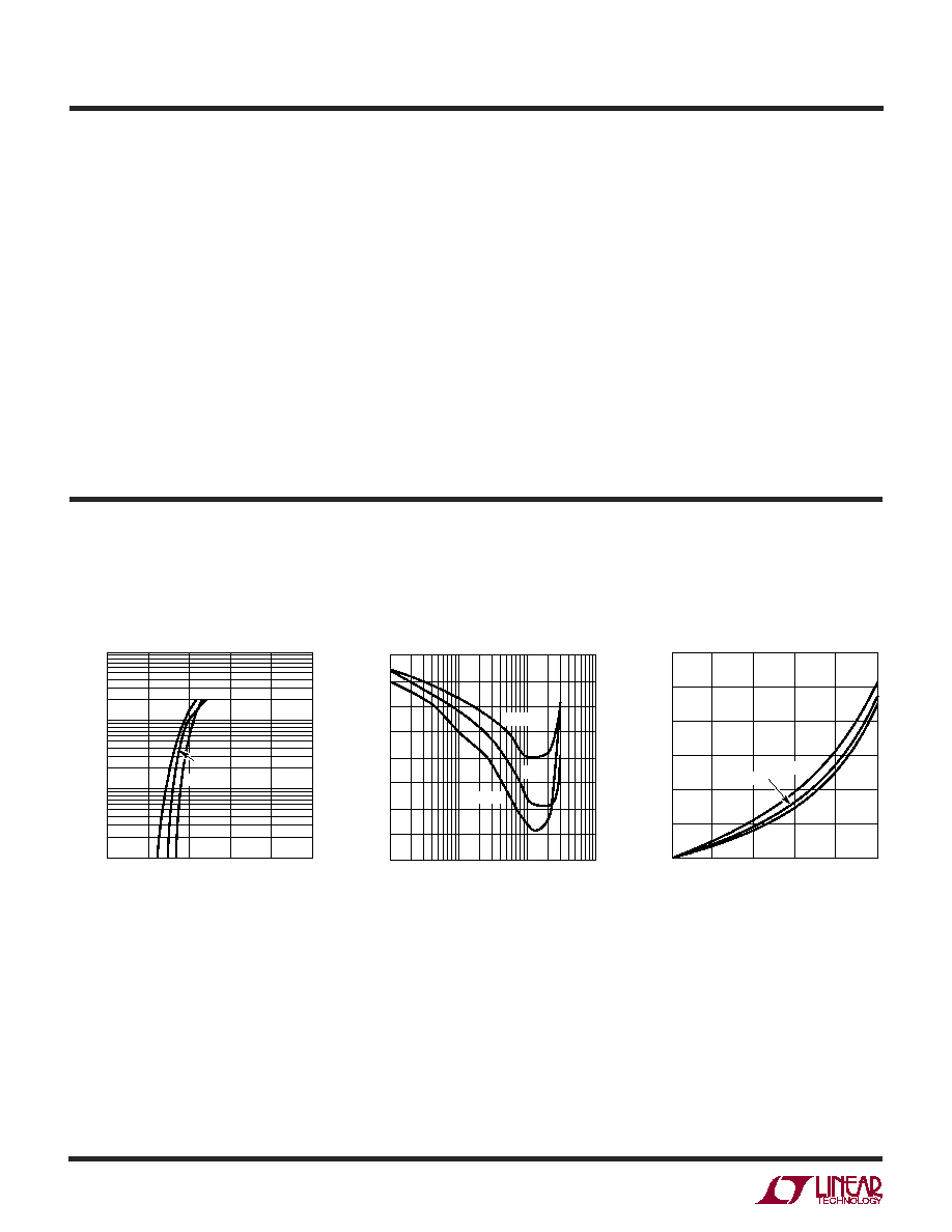
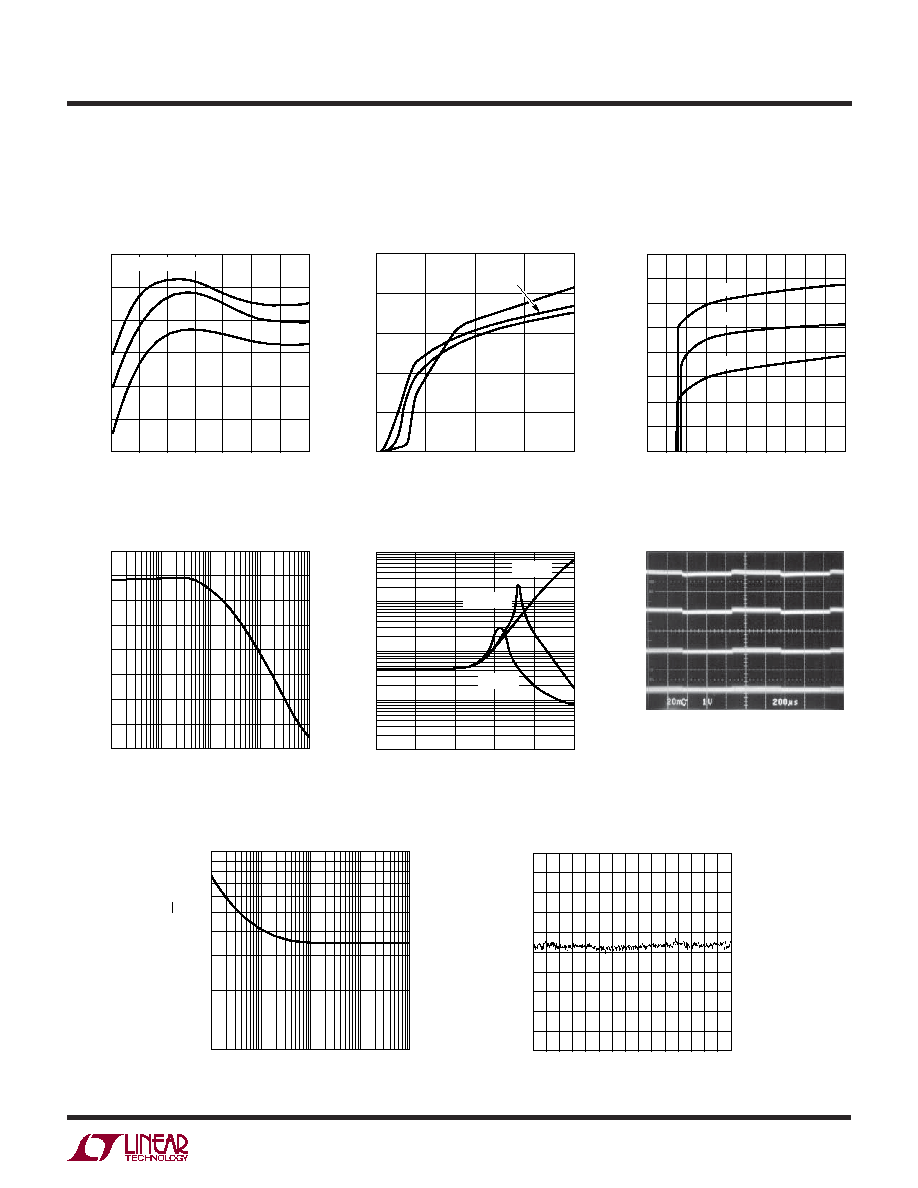
Characteristic curves are similar for most
LT1460S3s. Curves from the LT1460S3-2.5 and the LT1460-10 represent the extremes of the voltage options. Characteristic curves for
other output voltages fall between these curves, and can be estimated based on their voltage output.
INPUT-OUTPUT VOLTAGE (V)
0
0.1
OUTPUT CURRENT (mA)
10
125
°
C
25
°
C
100
0.5
1.0
1.5
2.0
2.5
1460S3 G01
1
55
°
C
OUTPUT CURRENT (mA)
0.1
2.0
OUTPUT VOLTAGE CHANGE (mV)
1.0
0
1
10
100
1460s3 G02
3.0
2.5
1.5
0.5
3.5
4.0
55
°
C
25
°
C
125
°
C
OUTPUT CURRENT (mA)
0
0
OUTPUT VOLTAGE CHANGE (mV)
20
40
60
80
100
120
1
2
3
4
55
°
C
1460S3 G03
5
125
°
C
25
°
C
5
LT1460S3 (SOT-23)
FREQUENCY (kHz)
1
OUTPUT IMPEDANCE (
)
10
100
1000
0.01
1
10
100
0.1
0.1
1000
1460S3 G08
C
L
= 0
µ
F
C
L
= 0.1
µ
F
C
L
= 1
µ
F
FREQUENCY (kHz)
20
POWER SUPPLY REJECTION RATIO (dB)
40
50
70
80
0.1
10
100
1000
1460S3 G07
0
1
60
30
10
2.5V Output Voltage
Temperature Drift
2.5V Supply Current
vs Input Voltage
2.5V Line Regulation
2.5V Power Supply Rejection
Ratio vs Frequency
2.5V Output Impedance
vs Frequency
2.5V Transient Response
2.5V Output Noise 0.1Hz to 10Hz
TYPICAL PERFOR
M
A
N
CE CHARACTERISTICS
U
W
Characteristic curves are similar for most
LT1460S3s. Curves from the LT1460S3-2.5 and the LT1460-10 represent the extremes of the voltage options. Characteristic curves for
other output voltages fall between these curves, and can be estimated based on their voltage output.
20
10
1
0.1
LOAD CURRENT (mA)
200
µ
s/DIV
1460S3 G09
C
LOAD
= 0
µ
F
INPUT VOLTAGE (V)
0
SUPPLY CURRENT (
µ
A)
100
150
125
°
C
25
°
C
55
°
C
20
1460S3 G05
50
0
5
10
15
250
200
INPUT VOLTAGE (V)
0
OUTPUT VOLTAGE (V)
2.502
2.501
2.500
2.499
2.498
2.497
2.496
2.495
2.494
16
1460S3 G06
4
8
12
20
14
2
6
10
18
25
°
C
125
°
C
55
°
C
TIME (2 SEC/DIV)
OUTPUT NOISE (20
µ
V/DIV)
1460S3 G11
TEMPERATURE (
°
C)
50
OUTPUT VOLTAGE (V)
2.501
2.502
2.503
25
75
1460S3 G04
2.500
2.499
25
0
50
100
125
2.498
2.497
THREE TYPICAL PARTS
2.5V Output Voltage
Noise Spectrum
FREQUENCY (Hz)
100
1000
10
1k
10k
1460
-2.5
G10
100
100k
NOISE VOLTAGE (nV/
Hz)