Äîêóìåíòàöèÿ è îïèñàíèÿ www.docs.chipfind.ru
1
LT1461-2.5
Micropower Precision
Low Dropout Series
Voltage Reference
s
Trimmed to High Accuracy: 0.04% Max
s
Low Drift: 3ppm/
°
C Max
s
Low Supply Current: 50
µ
A Max
s
Temperature Coefficient Guaranteed to 125
°
C
s
High Output Current: 50mA Min
s
Low Dropout Voltage: 300mV Max
s
Excellent Thermal Regulation
s
Power Shutdown
s
Thermal Limiting
s
Operating Temperature Range: 40
°
C to 125
°
C
s
Available in SO-8 Package
The LT
®
1461 is a low dropout micropower bandgap refer-
ence that combines very high accuracy and low drift with low
supply current and high output drive. This series reference
uses advanced curvature compensation techniques to obtain
low temperature coefficient and trimmed precision thin-film
resistors to achieve high output accuracy. The LT1461 draws
only 35
µ
A of supply current, making it ideal for low power and
portable applications, however its high 50mA output drive
makes it suitable for higher power requirements, such as
precision regulators.
In low power applications, a dropout voltage of less than
300mV ensures maximum battery life while maintaining full
reference performance. Line regulation is nearly immeasur-
able, while the exceedingly good load and thermal regulation
will not add significantly to system error budgets. The
shutdown feature can be used to switch full load currents and
can be used for system power down. Thermal shutdown
protects the part from overload conditions.
s
A/D and D/A Converters
s
Precision Regulators
s
Handheld Instruments
s
Power Supplies
, LTC and LT are registered trademarks of Linear Technology Corporation.
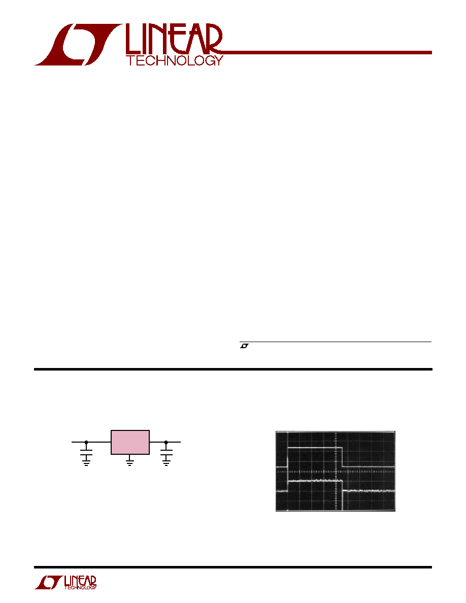
C
IN
1
µ
F
V
IN
2.8V
2.5V
C
L
2
µ
F
1461 TA01
LT1461-2.5
Load Regulation, P
DISS
= 200mW
Basic Connection
0mA
I
OUT
20mA
V
OUT
LOAD REG
1mV/DIV
10ms/DIV
1461 TA02
FEATURES
DESCRIPTIO
U
APPLICATIO S
U
TYPICAL APPLICATIO
U
2
LT1461-2.5
ABSOLUTE
M
AXI
M
U
M
RATINGS
W
W
W
U
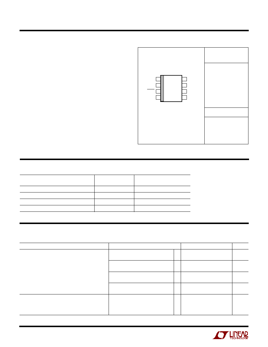
PACKAGE/ORDER I
N
FOR
M
ATIO
N
W
U
U
ORDER PART
NUMBER
LT1461ACS8-2.5
LT1461BCS8-2.5
LT1461CCS8-2.5
LT1461AIS8-2.5
LT1461BIS8-2.5
LT1461CIS8-2.5
LT1461DHS8-2.5
S8 PART MARKING
T
JMAX
= 130
°
C,
JA
= 190
°
C/ W
1
2
3
4
8
7
6
5
TOP VIEW
*DNC: DO NOT CONNECT
DNC*
DNC*
V
OUT
DNC*
DNC*
V
IN
SHDN
GND
S8 PACKAGE
8-LEAD PLASTIC SO
Consult factory for Military grade parts.
(Note 1)
Input Voltage ........................................................... 20V
Output Short-Circuit Duration ......................... Indefinite
Operating Temperature Range
(Note 2) ........................................... 40
°
C to 125
°
C
Specified Temperature Range
Commercial ............................................ 0
°
C to 70
°
C
Industrial ........................................... 40
°
C to 85
°
C
High ................................................. 40
°
C to 125
°
C
Storage Temperature Range (Note 3) ... 65
°
C to 150
°
C
Lead Temperature (Soldering, 10 sec).................. 300
°
C
PARAMETER
CONDITIONS
MIN
TYP
MAX
UNITS
Output Voltage (Note 4)
LT1461ACS8-2.5/LT1461AIS8-2.5
2.499
2.500
2.501
V
0.04
0.04
%
LT1461BCS8-2.5/LT1461BIS8-2.5
2.4985
2.500
2.5015
V
0.06
0.06
%
LT1461CCS8-2.5/LT1461CIS8-2.5
2.498
2.500
2.502
V
0.08
0.08
%
LT1461DHS8-2.5
2.49625
2.500
2.50375
V
0.15
0.15
%
Output Voltage Temperature Coefficient (Note 5)
LT1461ACS8-2.5/LT1461AIS8-2.5
q
1
3
ppm/
°
C
LT1461BCS8-2.5/LT1461BIS8-2.5
q
3
7
ppm/
°
C
LT1461CCS8-2.5/LT1461CIS8-2.5
q
5
12
ppm/
°
C
LT1461DHS8-2.5
q
7
20
ppm/
°
C
AVAILABLE OPTIO S
U
INITIAL
MAXIMUM TEMPERATURE
GRADE
ACCURACY (%)
COEFFICIENT (ppm/
°
C)
LT1461ACS8-2.5/LT1461AIS8-2.5
0.04%
3
LT1461BCS8-2.5/LT1461BIS8-2.5
0.06%
7
LT1461CCS8-2.5/LT1461CIS8-2.5
0.08%
12
LT1461DHS8-2.5, 40
°
C to 125
°
C
0.15%
20
ELECTRICAL CHARACTERISTICS
461A25
461B25
461C25
61AI25
61BI25
61CI25
61DH25
The
q
denotes specifications which apply over the specified temperature
range, otherwise specifications are at T
A
= 25
°
C. V
IN
V
OUT
= 0.5V, Pin 3 = 2.4V, C
L
= 2
µ
F, unless otherwise specified.
3
LT1461-2.5
PARAMETER
CONDITIONS
MIN
TYP
MAX
UNITS
Line Regulation
(V
OUT
+ 0.5V)
V
IN
20V
2
8
ppm/V
q
12
ppm/V
LT1461DHS8
q
15
50
ppm/V
Load Regulation Sourcing (Note 6)
V
IN
= V
OUT
+ 2.5V
0
I
OUT
50mA
12
30
ppm/mA
q
40
ppm/mA
LT1461DHS8, 0
I
OUT
10mA
q
50
ppm/mA
Dropout Voltage
V
IN
V
OUT
, V
OUT
Error = 0.1%
I
OUT
= 0mA
0.06
V
I
OUT
= 1mA
q
0.13
0.3
V
I
OUT
= 10mA
q
0.20
0.4
V
I
OUT
= 50mA, I and C Grades Only
q
1.50
2.0
V
Output Current
Short V
OUT
to GND
100
mA
Shutdown Pin
Logic High Input Voltage
q
2.4
V
Logic High Input Current, Pin 3 = 2.4V
q
2
15
µ
A
Logic Low Input Voltage
q
0.8
V
Logic Low Input Current, Pin 3 = 0.8V
q
0.5
4
µ
A
Supply Current
No Load
35
50
µ
A
q
70
µ
A
Shutdown Current
R
L
= 1k, Pin 3 = 0.8V
25
35
µ
A
q
55
µ
A
Output Voltage Noise (Note 7)
0.1Hz
f
10Hz
20
µ
V
P-P
8
ppm
P-P
10Hz
f
1kHz
24
µ
V
RMS
9.6
ppm
RMS
Long-Term Drift of Output Voltage, SO-8 Package (Note 8)
See Applications Information
60
ppm/
kHr
Thermal Hysteresis (Note 9)
T = 0
°
C to 70
°
C
40
ppm
T = 40
°
C to 85
°
C
70
ppm
T = 40
°
C to 125
°
C
120
ppm
ELECTRICAL CHARACTERISTICS
Note 1: Absolute Maximum Ratings are those values beyond which the life
of a device may be impaired.
Note 2: The LT1461 is guaranteed functional over the operating
temperature range of 40
°
C to 125
°
C.
Note 3: If the part is stored outside of the specified temperature range, the
output may shift due to hysteresis.
Note 4: ESD (Electrostatic Discharge) sensitive device. Extensive use of
ESD protection devices are used internal to the LT1461, however, high
electrostatic discharge can damage or degrade the device. Use proper ESD
handling precautions.
Note 5: Temperature coefficient is calculated from the minimum and
maximum output voltage measured at T
MIN
, Room and T
MAX
as follows:
TC = (V
OMAX
V
OMIN
)/(T
MAX
T
MIN
)
Incremental slope is also measured at 25
°
C.
Note 6: Load regulation is measured on a pulse basis from no load to the
specified load current. Output changes due to die temperature change
must be taken into account separately.
Note 7: Peak-to-peak noise is measured with a single pole highpass filter
at 0.1Hz and a 2-pole lowpass filter at 10Hz. The unit is enclosed in a still-
air environment to eliminate thermocouple effects on the leads. The test
time is 10 sec. RMS noise is measured with a single pole highpass filter at
10Hz and a 2-pole lowpass filter at 1kHz. The resulting output is full-wave
rectified and then integrated for a fixed period, making the final reading an
average as opposed to RMS. A correction factor of 1.1 is used to convert
from average to RMS and a second correction of 0.88 is used to correct
for the nonideal bandpass of the filters.
Note 8: Long-term drift typically has a logarithmic characteristic and
therefore, changes after 1000 hours tend to be much smaller than before
that time. Total drift in the second thousand hours is normally less than
one third that of the first thousand hours with a continuing trend toward
reduced drift with time. Long-term drift will also be affected by differential
stresses between the IC and the board material created during board
assembly.
See the Applications Information section.
Note 9: Hysteresis in output voltage is created by package stress that
depends on whether the IC was previously at a higher or lower
temperature. Output voltage is always measured at 25
°
C, but the IC is
cycled hot or cold before successive measurements. Hysteresis is roughly
proportional to the square of the temperature change. Hysteresis is not
normally a problem for operational temperature excursions where the
instrument might be stored at high or low temperature. See Applications
Information.
The
q
denotes specifications which apply over the specified temperature
range, otherwise specifications are at T
A
= 25
°
C. V
IN
V
OUT
= 0.5V, Pin 3 = 2.4V, C
L
= 2
µ
F, unless otherwise specified.
4
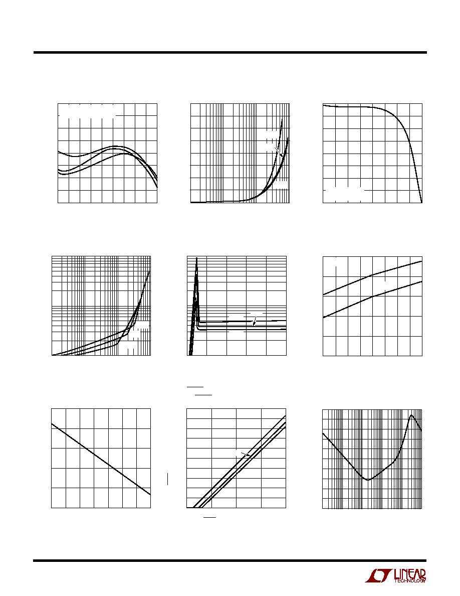
LT1461-2.5
TYPICAL PERFOR
M
A
N
CE CHARACTERISTICS
U
W
TEMPERATURE (
°
C)
60 40 20
2.4980
REFERENCE VOLTAGE (V)
2.4985
2.4995
2.5000
2.5005
60
80 100
1461 G01
2.4990
0
20
40
120
2.5010
2.5015
2.5020
TEMPCO 60
°
C TO 120
°
C
3 TYPICAL PARTS
Reference Voltage vs Temperature
TEMPERATURE (
°
C)
40 20
LINE REGULATION (ppm/V)
4
2
120
1461 G03
6
8
0
40
80
100
20
60
0
5
3
7
1
SUPPLY
= 15V
5V 20V
Line Regulation vs Temperature
Load Regulation
OUTPUT CURRENT (mA)
0.1
2
OUTPUT VOLTAGE CHANGE (mV)
3
4
1
10
100
1461 G02
1
0
125
°
C
25
°
C
55
°
C
Supply Current vs Temperature
TEMPERATURE (
°
C)
40
SUPPLY CURRENT (
µ
A)
30
40
50
I
S
20
60
120
1461 G06
20
10
0
20
0
40
80
100
I
S(SHDN)
V
IN
= 5V
Ripple Rejection Ratio
vs Frequency
FREQUENCY (kHz)
0.01
40
RIPPLE REJECTION RATIO (dB)
50
60
70
80
0.1
1
100
10
1000
1641 G01
30
20
10
0
90
100
Minimum Input/Output Voltage
Differential vs Load Current
OUTPUT CURRENT (mA)
0.1
0.1
INPUT/OUTPUT VOLTAGE (V)
1
10
1
10
100
1461 G04
55
°
C
25
°
C
125
°
C
Current Limit vs Temperature
TEMPERATURE (
°
C)
50
25
40
CURRENT LIMIT (mA)
80
140
0
50
75
1461 G07
60
120
100
25
100
125
Supply Current vs Input Voltage
INPUT VOLTAGE (V)
SUPPLY CURRENT (
µ
A)
1000
1461 G05
10
100
5
25
20
15
10
0
125
°
C
55
°
C
25
°
C
SHDN Pin Current
vs SHDN Input Voltage
SHDN PIN INPUT VOLTAGE (V)
0
0
SHDN PIN CURRENT (
µ
A)
20
60
80
100
200
140
10
1461 G08
40
160
125
°
C
55
°
C
180
120
5
15
20
25
°
C
5
LT1461-2.5
TYPICAL PERFOR
M
A
N
CE CHARACTERISTICS
U
W
Turn-On Time
Output Impedance vs Frequency
FREQUENCY (kHz)
0.01
1
OUTPUT IMPEDANCE (
)
10
100
1000
0.1
1
10
1461 G10
C
OUT
= 2
µ
F
C
OUT
= 1
µ
F
TIME (100
µ
s/DIV)
VOLTAGE (V)
V
IN
20
10
0
2
1
0
1461 G12
C
IN
= 1
µ
F
C
L
= 2
µ
F
R
L
= 50
V
OUT
Turn-On Time
TIME (100
µ
s/DIV)
VOLTAGE (V)
V
IN
20
10
0
2
1
0
1461 G11
C
IN
= 1
µ
F
C
L
= 2
µ
F
R
L
=
V
OUT
Transient Response to 10mA
Load Step
I
OUT
0mA
10mA/DIV
V
OUT
50mV/DIV
1461 G13
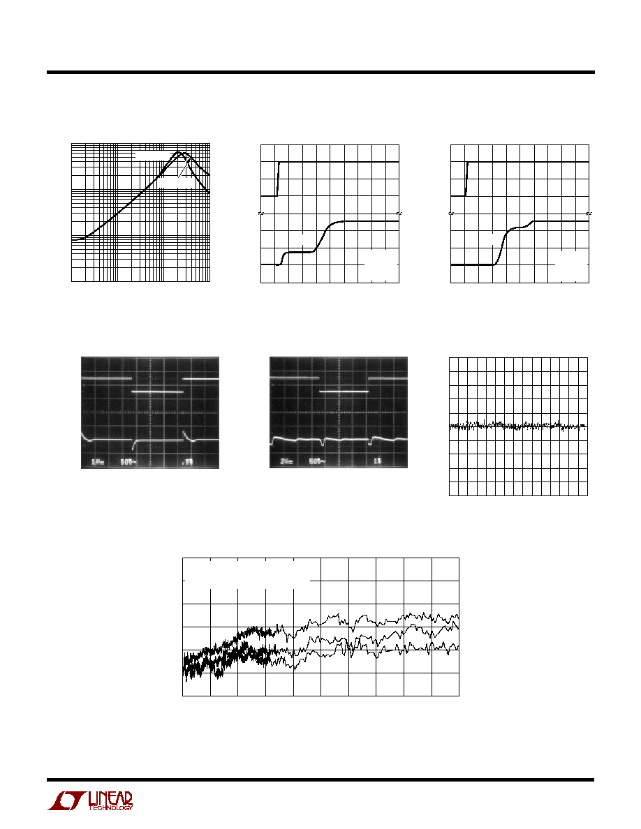
Long-Term Drift (Number of Data Points Reduced at 650 Hours)*
Line Transient Response
5V
4V
V
IN
V
OUT
50mV/DIV
1461 G14
C
IN
= 0.1
µ
F
Output Noise 0.1Hz
f
10Hz
TIME (2SEC/DIV)
OUTPUT NOISE (20
µ
V/DIV)
1461 G18
HOURS
50
ppm
50
150
250
0
100
200
400
800
1200
1600
1461 G15
2000
200
600
1000
1400
1800
0
LT1461S8-2.5
3 TYPICAL PARTS SOLDERED ONTO PCB
T
A
= 30
°
C
C
L
= 2
µ
F
*SEE APPLICATIONS INFORMATION FOR DETAILED EXPLANATION OF LONG-TERM DRIFT