 | ÐлекÑÑоннÑй компоненÑ: LT1463CN | СкаÑаÑÑ:  PDF PDF  ZIP ZIP |
Äîêóìåíòàöèÿ è îïèñàíèÿ www.docs.chipfind.ru
1
LT1462/LT1463
Dual/Quad Micropower,
260
µ
W C-Load Picoampere
Bias Current JFET Input Op Amps
s
Input Bias Current:
2pA Max (LT1462A)
20pA Max (LT1462, LT1463)
s
Supply Current per Amplifier: 45
µ
A Max
s
Unity-Gain Stable for C-Load
TM
Up to 10nF
s
Input Common Mode Range Includes Positive Rail
s
Guaranteed Specs with
±
5V,
±
15V Supplies
s
Gain Bandwidth Product: 175kHz Typ
s
Slew Rate: 0.13V/
µ
s Typ
s
Guaranteed Matching Specifications
s
Standard Pinout: SO-8, SO-14 Package
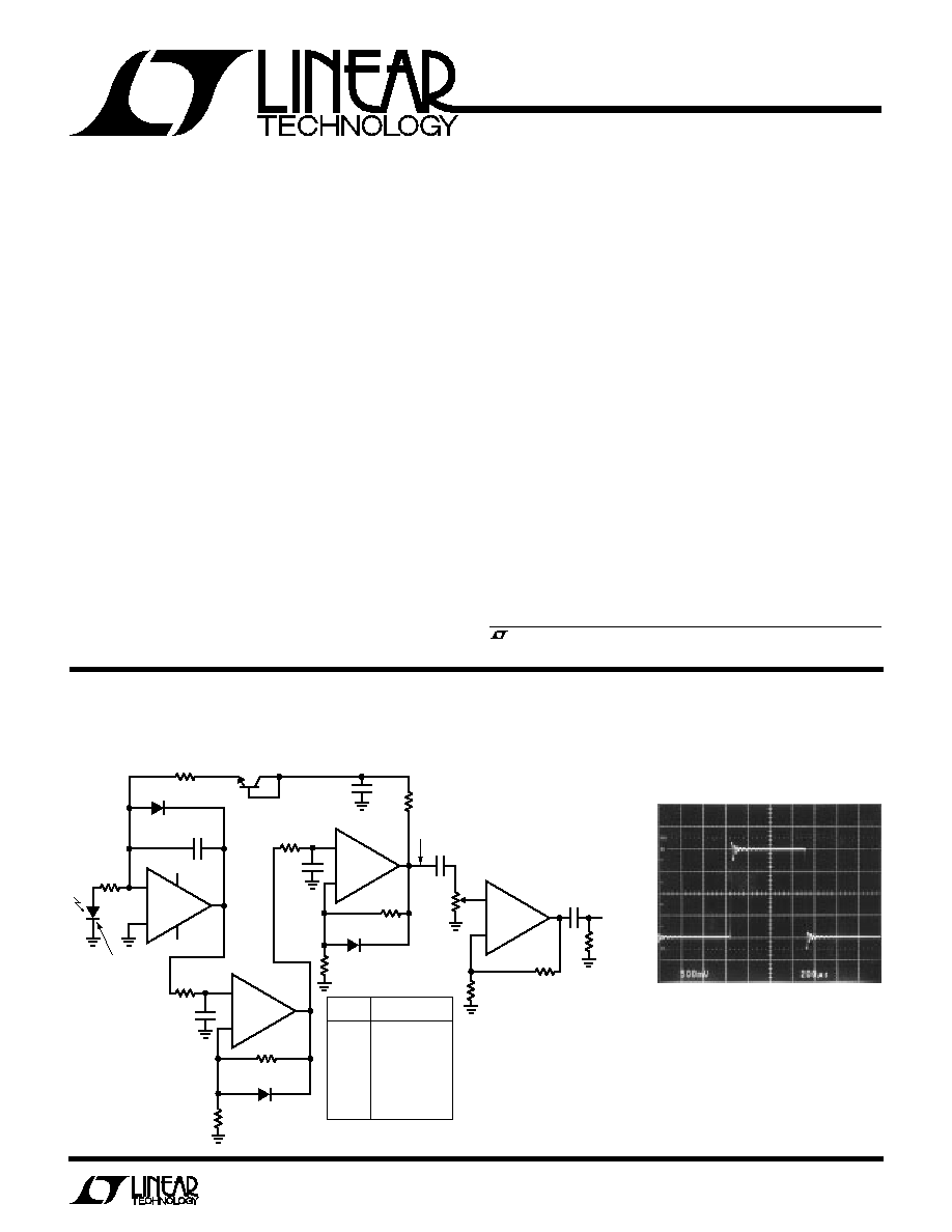
The LT
®
1462 (dual) and LT1463 (quad) are the first
micropower op amps (45
µ
A max per amp) to offer
picoampere input bias currents (1pA typ) and unity gain
stability for capacitive loads up to 10nF. The output can
swing a 10k load to within 1.5V of either supply, just like
op amps that require an order of magnitude more supply
current. This unique combination of performance makes
the LT1462/LT1463 ideal over a wide range of input and
output impedances.
In the design and testing of the LT1462/LT1463, particular
emphasis has been placed on optimizing performance in
the low cost SO-8 (dual) and 14-lead SO package (quad) for
±
15V and
±
5V supplies. The input common mode range
includes the positive rail. Slew rate (0.08V/
µ
s min) and gain
bandwidth product (125kHz min) are 100% tested. A full set
of matching specifications is also provided.
FEATURES
DESCRIPTIO
N
U
TYPICAL APPLICATIO
N
U
, LTC and LT are registered trademarks of Linear Technology Corporation.
+
+
+
+
R3
10k
C4
10
µ
F
R11
1M
1/4 LT1463
8
10
9
R12
10k
R10
50k
R6
100k
D3
1N4148
R7
10M
R5
24k
C5
200pF
AMP 3
1/4 LT1463
DC
OUT C3
0.47
µ
F
5
6
7
R3
100k
D2
1N4148
R4
10M
1/4 LT1463
1/4 LT1463
C2
200pF
R2
24k
14
12
13
2
3
4
11
1
5V
5V
R1
100
PHOTODIODE
C1
1nF
D1
1N4148
R8
100k
Q1
2N3904
C5
1
µ
F
R9
1M
1462 · TA01
AC
OUT
INPUT
DC OUTPUT
CURRENT VOLTAGE OF AMP 3
10pA
0.145V
100pA
0.341V
1nA
0.518V
10nA
0.684V
100nA
0.846V
1
µ
A
0.995V
10
µ
A
1.13V
100
µ
A
1.25V
1mA
1.37V
Low Power Logging Amplifier
A
V
= 1
V
S
=
±
5V,
±
15V
C
L
= 10nF
1462 · TA02
C-Load is a trademark of Linear Technology Corporation.
Small-Signal Response, C
L
= 10nF
s
Battery-Powered Systems
s
Photocurrent Amplifiers
s
Low Frequency, Micropower Active Filters
s
Low Droop Track-and-Hold Circuits
APPLICATIO
N
S
U
2
LT1462/LT1463
ABSOLUTE
M
AXI
M
U
M
RATINGS
W
W
W
U
Supply Voltage .....................................................
±
20V
Differential Input Voltage .......................................
±
40V
Input Current ....................................................... 20mA
Output Short-Circuit Duration ......................... Indefinite
Operating Temperature Range ............... 40
°
C to 85
°
C
Specified Temperature Range ................ 40
°
C to 85
°
C
Maximum Junction Temperature ......................... 150
°
C
Storage Temperature Range ................ 65
°
C to 150
°
C
Lead Temperature (Soldering, 10 sec).................. 300
°
C
PACKAGE/ORDER I
N
FOR
M
ATIO
N
W
U
U
ORDER PART
NUMBER
LT1463CN
LT1463CS
ORDER PART
NUMBER
LT1462ACN8
LT1462ACS8
LT1462CN8
LT1462CS8
1462
1462A
ELECTRICAL CHARACTERISTICS
V
S
=
±
15V, V
CM
= 0V, T
A
= 25
°
C, unless otherwise noted.
LT1462AC
LT1462C/LT1463C
SYMBOL
PARAMETER
CONDITIONS (Note 1)
MIN
TYP
MAX
MIN
TYP
MAX
UNITS
V
OS
Input Offset Voltage
V
S
=
±
5V
0.4
0.8
0.4
0.8
mV
V
S
=
±
15V
0.6
2.0
0.6
2.0
mV
I
OS
Input Offset Current
V
S
=
±
5V
0.3
1.2
pA
V
S
=
±
15V
0.5
2.0
0.5
15
pA
I
B
Input Bias Current
V
S
=
±
5V
±
0.5
±
2.0
pA
V
S
=
±
15V
±
1
±
3.0
±
1
±
20
pA
e
n
Input Noise Voltage
0.1Hz to 10Hz
2
2
µ
V
P-P
Input Noise Voltage Density
f
O
= 10Hz
92
92
nV/
Hz
f
O
= 1000Hz
76
76
nV/
Hz
Input Noise Current Density
f
O
= 10Hz, 1kHz (Note 3)
0.5
0.5
fA/
Hz
CMRR
Common Mode Rejection Ratio
V
CM
= 12.5V to 15V
76
89
74
89
dB
PSRR
Power Supply Rejection Ratio
V
S
=
±
2.5V to
±
20V
81
90
78
90
dB
R
IN
Input Resistance--Differential
10
12
10
12
Common Mode
V
CM
= 12.5V to 8V
10
12
10
12
Common Mode
V
CM
= 8V to 15V
10
11
10
11
C
IN
Input Capacitance
3
3
pF
A
VOL
Large-Signal Voltage Gain
V
O
=
±
10V, R
L
= 10k
100
600
100
600
V/mV
V
S
=
±
5V, V
O
=
±
2V, R
L
= 10k
50
200
50
200
V/mV
1
2
3
4
8
7
6
5
TOP VIEW
V
+
OUT B
IN B
+IN B
OUT A
IN A
+IN B
V
S8 PACKAGE
8-LEAD PLASTIC SO
N8 PACKAGE
8-LEAD PDIP
B
A
T
JMAX
= 150
°
C,
JA
= 130
°
C/ W (N)
T
JMAX
= 150
°
C,
JA
= 190
°
C/ W (S)
TOP VIEW
S PACKAGE
14-LEAD PLASTIC SO
N PACKAGE
14-LEAD PDIP
1
2
3
4
5
6
7
14
13
12
11
10
9
8
OUT A
IN A
+IN A
V
+
+IN B
IN B
OUT B
OUT D
IN D
+IN D
V
+IN C
IN C
OUT C
A
B
D
C
T
JMAX
= 150
°
C,
JA
= 110
°
C/ W (N)
T
JMAX
= 150
°
C,
JA
= 150
°
C/ W (S)
Consult factory for Industrial and Military grade parts.
S8 PART MARKING
3
LT1462/LT1463
ELECTRICAL CHARACTERISTICS
V
S
=
±
15V, V
CM
= 0V, T
A
= 25
°
C, unless otherwise noted.
V
S
=
±
15V, V
CM
= 0V, 0
°
C
T
A
70
°
C, unless otherwise noted.
LT1462AC
LT1462C/LT1463C
SYMBOL
PARAMETER
CONDITIONS (Note 1)
MIN
TYP
MAX
MIN
TYP
MAX
UNITS
V
OUT
Output Voltage Swing
R
L
= 10k
±
13.5
±
13.7
±
13.5
±
13.7
V
R
L
= 2k
±
11.0
±
12.4
±
11.0
±
12.4
V
V
S
=
±
5V, R
L
= 2k
±
3.5
±
3.7
±
3.5
±
3.7
V
I
O
Output Current
±
13
±
17
±
13
±
17
mA
SR
Slew Rate
R
L
= 10k (Note 4)
0.08
0.13
0.08
0.13
V/
µ
s
GBW
Gain Bandwidth Product
f = 10kHz
125
175
125
175
kHz
I
S
Supply Current per Amplifier
28
45
28
45
µ
A
V
S
=
±
5V
26
43
26
43
µ
A
Channel Separation
f = 10Hz, V
O
=
±
10V, R
L
= 10k
132
132
dB
V
OS
Offset Voltage Match (Note 7)
V
S
=
±
5V
0.5
1.3
0.5
1.3
mV
V
S
=
±
15V
0.8
3.0
0.8
3.0
mV
I
B
+
Noninverting Bias Current Match
V
S
=
±
5V
0.4
3.0
pA
(Note 7)
V
S
=
±
15V
0.5
4.0
0.5
20
pA
CMRR
Common Mode Rejection Match
(Notes 5, 7)
74
85
72
85
dB
PSRR
Power Supply Rejection Match
(Notes 5, 7)
78
88
76
88
dB
LT1462AC
LT1462C/LT1463C
SYMBOL
PARAMETER
CONDITIONS (Note 1)
MIN
TYP
MAX
MIN
TYP
MAX
UNITS
V
OS
Input Offset Voltage
V
S
=
±
5V
q
0.5
1.4
0.5
1.4
mV
V
S
=
±
15V
q
0.9
2.8
0.9
2.8
mV
V
OS
Average Input Offset Voltage Drift
(Note 6)
q
7
20
7
20
µ
V/
°
C
Temp
I
OS
Input Offset Current
q
10
50
25
450
pA
I
B
Input Bias Current
q
60
150
150
750
pA
CMRR
Common Mode Rejection Ratio
V
CM
= 12V to 15V
q
75
88
72
88
dB
PSRR
Power Supply Rejection Ratio
V
S
=
±
3V to
±
20V
q
80
89
76
89
dB
A
VOL
Large-Signal Voltage Gain
V
O
=
±
10V, R
L
= 10k
q
90
600
90
600
V/mV
V
S
=
±
5V, V
O
=
±
2V, R
L
= 2k
q
45
140
45
140
V/mV
I
O
Output Current
q
±
11
±
14
±
11
±
14
mA
V
OUT
Output Voltage Swing
R
L
= 10k
q
±
13.4
±
13.6
±
13.4
±
13.6
V
R
L
= 2k
q
±
10.5
±
12.1
±
10.5
±
12.1
V
V
S
=
±
5V, R
L
= 2k
q
±
3.4
±
3.6
±
3.4
±
3.6
V
SR
Slew Rate
R
L
= 10k (Note 4)
q
0.075
0.128
0.075
0.128
V/
µ
s
GBW
Gain Bandwidth Product
f = 10kHz
q
100
140
100
140
kHz
I
S
Supply Current per Amplifier
q
31
45
31
45
µ
A
V
S
=
±
5V
q
28
43
28
43
µ
A
V
OS
Offset Voltage Match (Note 7)
V
S
=
±
5V
q
0.7
2.0
0.7
2.0
mV
V
S
=
±
15V
q
0.9
3.5
0.9
3.5
mV
I
B
+
Noninverting Bias Current Match
q
5
40
35
500
pA
(Note 7)
4
LT1462/LT1463
ELECTRICAL CHARACTERISTICS
LT1462AC
LT1462C/LT1463C
SYMBOL
PARAMETER
CONDITIONS (Note 1)
MIN
TYP
MAX
MIN
TYP
MAX
UNITS
CMRR
Common Mode Rejection Match
(Notes 5, 7)
q
73
84
70
84
dB
PSRR
Power Supply Rejection Match
(Notes 5, 7)
q
77
87
74
87
dB
V
S
=
±
15V, V
CM
= 0V, 40
°
C
T
A
85
°
C (Note 2), unless otherwise noted.
LT1462AC
LT1462C/LT1463C
SYMBOL
PARAMETER
CONDITIONS (Note 1)
MIN
TYP
MAX
MIN
TYP
MAX
UNITS
V
OS
Input Offset Voltage
V
S
=
±
5V
q
0.6
1.5
0.6
1.5
mV
V
S
=
±
15V
q
1.0
3.0
1.0
3.0
mV
V
OS
Average Input Offset Voltage Drift
(Note 6)
q
7
20
7
20
µ
V/
°
C
Temp
I
OS
Input Offset Current
q
40
150
60
700
pA
I
B
Input Bias Current
q
200
500
300
2500
pA
CMRR
Common Mode Rejection Ratio
V
CM
= 12V to 15V
q
74
87
70
87
dB
PSRR
Power Supply Rejection Ratio
V
S
=
±
3V to
±
20V
q
79
88
74
88
dB
A
VOL
Large-Signal Voltage Gain
V
O
=
±
10V, R
L
= 10k
q
80
500
80
500
V/mV
V
S
=
±
5V, V
O
=
±
2V, R
L
= 2k
q
40
120
40
120
V/mV
I
O
Output Current
q
±
10
±
13
±
10
±
13
mA
V
OUT
Output Voltage Swing
R
L
= 10k
q
±
13.2
±
13.4
±
13.2
±
13.4
V
R
L
= 2k
q
±
10.0
±
11.8
±
10.0
±
11.8
V
V
S
=
±
5V, R
L
= 2k
q
±
3.2
±
3.4
±
3.2
±
3.4
V
SR
Slew Rate
R
L
= 10k (Note 4)
q
0.070
0.126
0.070
0.126
V/
µ
s
GBW
Gain Bandwidth Product
f = 10kHz
q
95
135
95
135
kHz
I
S
Supply Current per Amplifier
q
33
50
33
50
µ
A
V
S
=
±
5V
q
31
48
31
48
µ
A
V
OS
Offset Voltage Match (Note 7)
V
S
=
±
5V
q
0.8
2.5
0.8
2.5
mV
V
S
=
±
15V
q
1.0
4.0
1.0
4.0
mV
I
B
+
Noninverting Bias Current Match
q
20
100
70
800
pA
(Note 7)
CMRR
Common Mode Rejection Match
(Notes 5, 7)
q
72
83
68
83
dB
PSRR
Power Supply Rejection Match
(Notes 5, 7)
q
76
86
72
86
dB
V
S
=
±
15V, V
CM
= 0V, 0
°
C
T
A
70
°
C, unless otherwise noted.
The
q
denotes specifications which apply over the full operating
temperature range.
Note 1: Typical parameters are defined as 60% yield of parameter
distributions of individual amplifiers, i.e., out of 100 LT1463s (or 100
LT1462s) typically 240 op amps (or 120) will be better than the indicated
specification.
Note 2: The LT1462 and LT1463 are designed, characterized and expected
to meet these extended temperature limits, but are not tested at 40
°
C
and 85
°
C. Guaranteed I grade parts are available, consult factory.
Note 3: Current noise is calculated from the formula: i
n
= (2qi
b
)
1/2
where
q = (1.6)(10
19
) coulomb. The noise of source resistors up to 1G swamps
the contribution of current noise.
Note 4: Slew rate is measured in A
V
= 1; input signal is
±
7.5V, output is
measured at
±
2.5V.
Note 5:
CMRR and
PSRR are defined as follows:
1. CMRR and PSRR are measured in
µ
V/V on the individual amplifiers.
2. The difference is calculated between the matching sides in
µ
V/V.
3. The result is converted to dB.
Note 6: This parameter is not 100% tested.
Note 7: Matching parameters are the difference between amplifiers A and
D and between B and C on the LT1463; between the two amplifiers on the
LT1462.
5
LT1462/LT1463
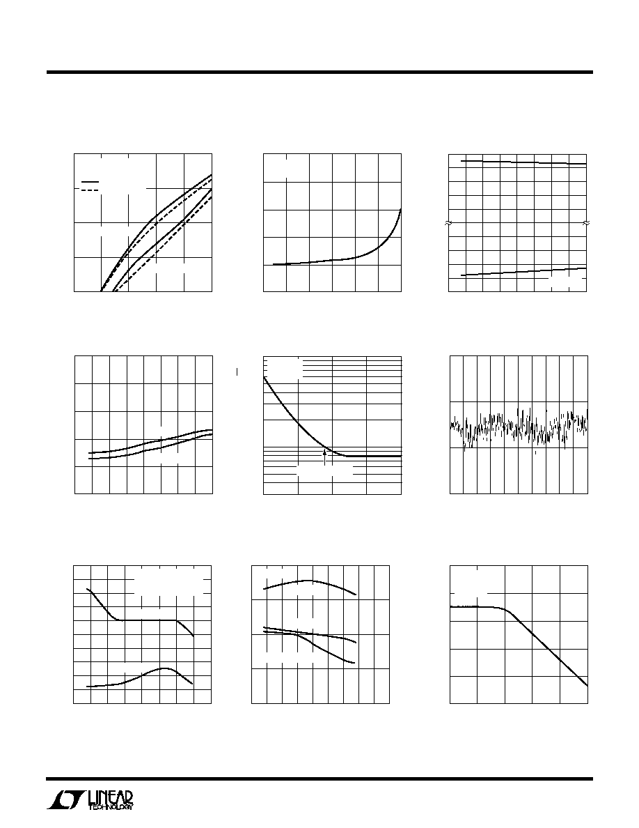
TYPICAL PERFOR
M
A
N
CE CHARACTERISTICS
U
W
Voltage Noise vs Frequency
FREQUENCY (Hz)
1
30
100
1000
10
100
LT1462 · TPC05
RMS VOLTAGE NOISE DENSITY (nV/
Hz)
0.1
1000
V
S
=
±
15V
T
A
= 25
°
C
1/f CORNER = 5Hz
0.1Hz to 10Hz Noise
TIME (SEC)
0
NOISE VOLTAGE (2
µ
V/DIV)
8
LT1462 · TPC06
2
4
6
10
FREQUENCY (Hz)
10
CHANNEL SEPARATION (dB)
160
140
120
100
80
60
100k
LT1462 · TPC09
100
1k
10k
1M
V
S
=
±
15V
T
A
= 25
°
C
R
L
= 10k
Channel Separation vs Frequency
Slew Rate, Gain Bandwidth
Product vs Temperature
TEMPERATURE (
°
C)
75
0.09
SLEW RATE (V/
µ
s)
GAIN BANDWIDTH (kHz)
0.11
0.13
0.15
0.17
0
100
200
300
400
50 25
0
25
LT1462 · TPC08
50
75 100 125 150
V
S
=
±
15V
SLEW RISE
SLEW FALL
GAIN BANDWIDTH
Input Bias and Offset Current vs
Temperature
Supply Current vs Temperature
Voltage Gain vs Temperature
AMBIENT TEMPERATURE (
°
C)
0
INPUT BIAS AND OFFSET CURRENT (pA)
100
LT1462 · TPC01
25
50
75
125
10000
1000
100
10
1
LT1462/LT1463
LT1462A
OFFSET CURRENT
BIAS CURRENT
V
S
=
±
15V
V
CM
= 0V
TEMPERATURE (
°
C)
75
SUPPLY CURRENT PER AMPLIFIER (
µ
A)
40
50
60
0
50
125
LT1462 · TPC04
30
20
10
50 25
25
75
100
V
S
=
±
15V
V
S
=
±
5V
TEMPERATURE (
°
C)
75
VOLTAGE GAIN (V/mV)
1000
900
800
700
600
500
400
300
200
100
0
25
25
50
LT1463 · TPC07
50
0
75
100
125
V
S
=
±
15V
V
S
=
±
5V
V
O
=
±
10V, V
S
=
±
15V
V
O
=
±
2V, V
S
=
±
5V
R
L
= 10k
COMMON MODE INPUT VOLTAGE (V)
15
5
INPUT BIAS CURRENT (pA)
0
5
10
15
20
10
5
0
5
LT1462 · TPC02
10
15
V
S
=
±
15V
T
A
= 25
°
C
TEMPERATURE (
°
C)
75
COMMON MODE RANGE (V)
16
15
14
13
12
11
12
13
14
15
25
25
50
LT1462 · TPC03
50
0
75
100
125
V
S
=
±
15V
Common Mode Range vs
Temperature
Input Bias Current Over the
Common Mode Range