 | ÐлекÑÑоннÑй компоненÑ: LT1467L | СкаÑаÑÑ:  PDF PDF  ZIP ZIP |
Äîêóìåíòàöèÿ è îïèñàíèÿ www.docs.chipfind.ru
1
LT1466L/LT1467L
Micropower Dual/Quad
Precision Rail-to-Rail Input
and Output Op Amps
s
Rail-to-Rail Input and Output
s
Low Supply Current: 75
µ
A Max
s
390
µ
V V
OS(MAX)
for V
CM
= V
to V
+
s
High Common Mode Rejection Ratio: 83dB Min
s
High A
VOL
: 400V/mV Min
s
Wide Supply Range: 2V to
±
5V
s
Low Input Bias Current: 6nA Typ
s
120kHz Gain Bandwidth Product
FEATURES
DESCRIPTIO
N
U
The LT
®
1466L/LT1467L are dual/quad bipolar op amps
that combine rail-to-rail input and output operation with
precision specifications. Using a patented technique,
both input stages of the LT1466L/LT1467L are trimmed:
one at the negative supply and the other at the positive
supply. The resulting common mode rejection of 83dB
minimum is much better than other rail-to-rail input op
amps. A minimum open-loop gain of 400V/mV into a 10k
load virtually eliminates all gain error. Operation is speci-
fied for 3V, 5V and
±
5V supplies.
Unlike other rail-to-rail amplifiers, the input offset voltage
of 390
µ
V maximum is guaranteed across the entire rail-to-
rail input range, not just at half supply. The graph below
contrasts the V
OS
specifications of the LT1466L/LT1467L
to a competitive part that is specified only at half supply.
As can be seen, the LT1466L/LT1467L's limits are much
tighter for inputs near either supply.
The LT1466L is available in 8-lead PDIP and SO-8 pack-
ages with the standard dual pinout. The LT1467L features
the standard quad pinout and is available in a 16-lead
narrow SO package.
APPLICATIO
N
S
U
s
Supply Current Sensing
s
Driving A/D Converters
s
Test Equipment Amplifiers
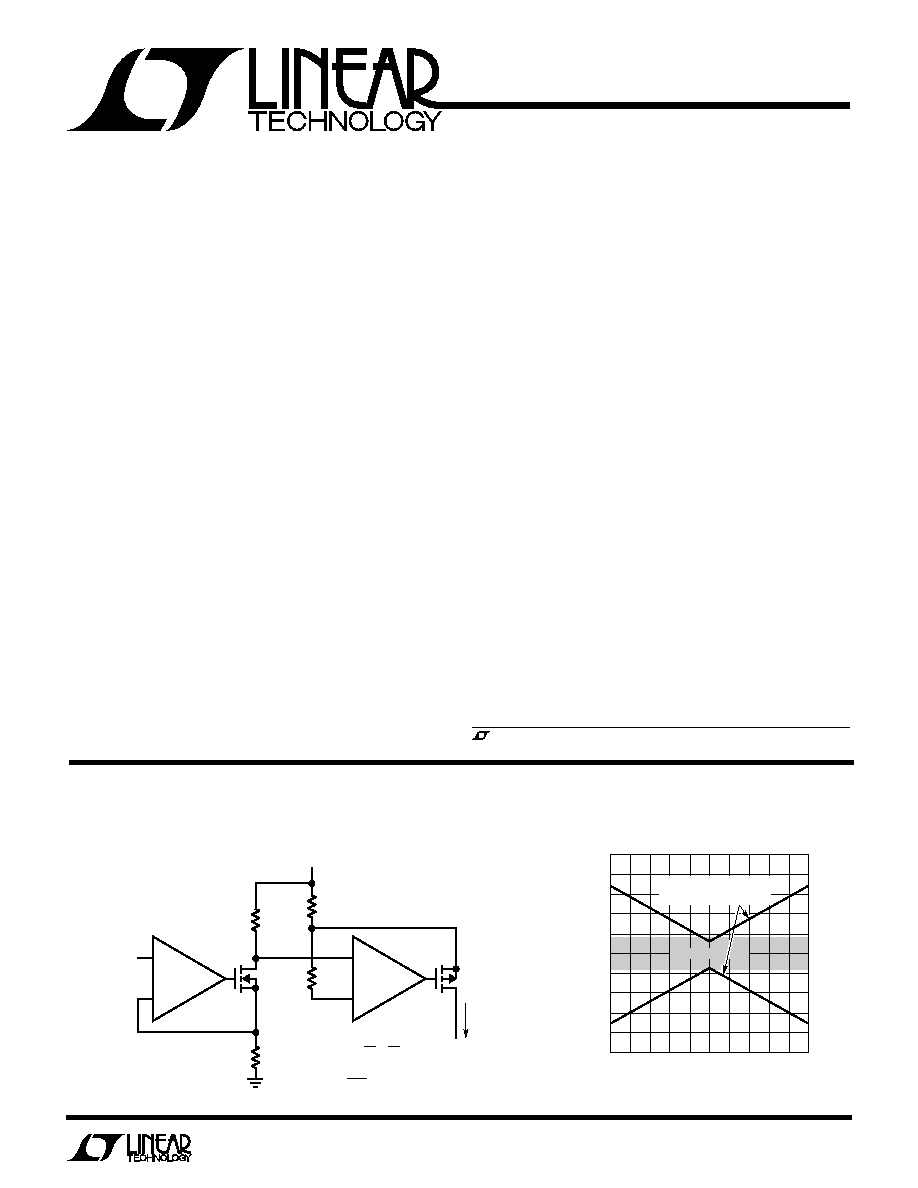
Worst-Case V
OS
vs Input Common Mode Voltage
, LTC and LT are registered trademarks of Linear Technology Corporation.
TYPICAL APPLICATIO
N
U
+
+
1/2 LT1466L
1/2 LT1466L
VN2222
10k
R1
100k
R2
10k
R3
5.1
V
CC
TP0610
V
IN
0V TO 2.5V
I
O
I
O
= V
IN
R2
R1
( )
1
R3
( )
=
V
IN
51
( )
1466L/67L TA01
Variable Current Source
INPUT COMMON MODE VOLTAGE (V)
0
INPUT OFFSET VOLTAGE (
µ
V)
1466L/67L TA02
0
1000
2000
1000
2000
2
4
1
3
5
LT1467L LIMITS
TYPICAL RAIL-TO-RAIL
AMPLIFIER (65dB CMRR)
2
LT1466L/LT1467L
ABSOLUTE
M
AXI
M
U
M
RATINGS
W
W
W
U
Supply Voltage ........................................................
±
8V
Input Current ......................................................
±
15mA
Output Short-Circuit Duration (Note 1) .........Continuous
Specified Temperature Range ...................... 0
°
C to 70
°
C
Junction Temperature ........................................... 150
°
C
Storage Temperature Range ................. 65
°
C to 150
°
C
Lead Temperature (Soldering, 10 sec) .................. 300
°
C
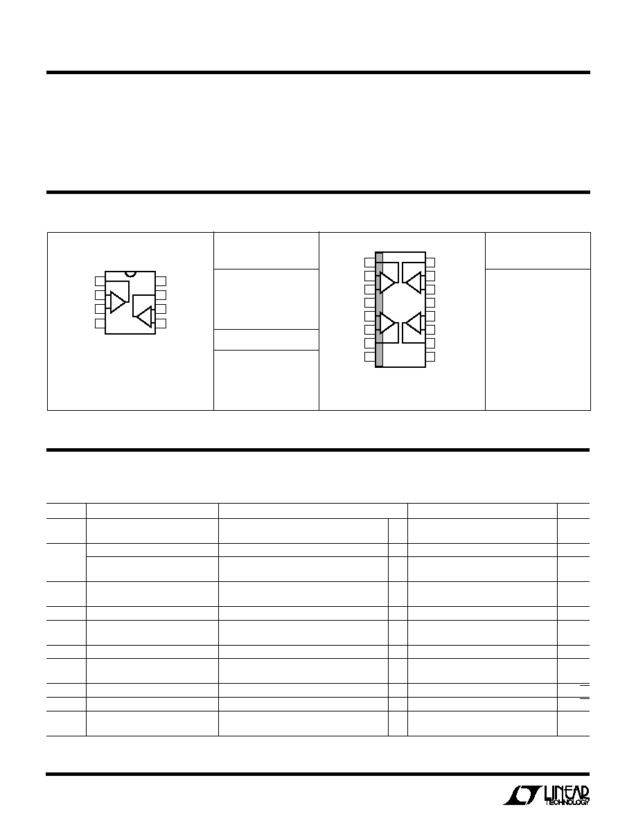
PACKAGE/ORDER I
N
FOR
M
ATIO
N
W
U
U
ORDER PART
NUMBER
LT1467LCS
T
JMAX
= 150
°
C,
JA
= 150
°
C/ W
ORDER PART
NUMBER
LT1466LCN8
LT1466LCS8
S8 PART MARKING
1466L
TOP VIEW
S PACKAGE
16-LEAD PLASTIC SO
1
2
3
4
5
6
7
8
16
15
14
13
12
11
10
9
OUT A
IN A
+ IN A
V
+
+ IN B
IN B
OUT B
NC
OUT D
IN D
+ IN D
V
+ IN C
IN C
OUT C
NC
A
D
B
C
T
JMAX
= 150
°
C,
JA
= 130
°
C/ W (N)
T
JMAX
= 150
°
C,
JA
= 190
°
C/ W (S)
Consult factory for Industrial and Military grade parts.
SYMBOL
PARAMETER
CONDITIONS
MIN
TYP
MAX
UNITS
V
OS
Input Offset Voltage
V
CM
= V
+
110
390
µ
V
V
CM
= V
110
390
µ
V
V
OS
Input Offset Voltage Shift
V
CM
= V
to V
+
75
345
µ
V
Input Offset Voltage Match
V
CM
= V
, V
+
(Notes 3, 4)
150
550
µ
V
(Channel-to-Channel)
I
B
Input Bias Current
V
CM
= V
+
3
14
nA
V
CM
= V
14
6
nA
I
B
Input Bias Current Shift
V
CM
= V
to V
+
9
28
nA
I
OS
Input Offset Current
V
CM
= V
+
0.6
3.6
nA
V
CM
= V
0.4
3.6
nA
I
OS
Input Offset Current Shift
V
CM
= V
to V
+
0.9
5.1
nA
Input Bias Current Match
V
CM
= V
+
(Note 4)
0.6
5.1
nA
(Channel-to-Channel)
V
CM
= V
(Note 4)
0.6
5.1
nA
e
n
Input Noise Voltage Density
f = 1kHz
45
nV/
Hz
i
n
Input Noise Current Density
f = 1kHz
0.05
pA/
Hz
A
VOL
Large-Signal Voltage Gain
V
S
= 5V, V
O
= 0.5V to 4.4V, R
L
= 10k
400
1500
V/mV
V
S
= 3V, V
O
= 0.5V to 2.4V, R
L
= 10k
250
1000
V/mV
T
A
= 25
°
C, V
S
= 5V, 0V; V
S
= 3V, 0V; V
CM
= V
O
= half supply, unless otherwise noted.
ELECTRICAL CHARACTERISTICS
1
2
3
4
8
7
6
5
TOP VIEW
OUT A
IN A
+IN A
V
V
+
OUT B
IN B
+IN B
N8 PACKAGE
8-LEAD PDIP
S8 PACKAGE
8-LEAD PLASTIC SO
A
B
3
LT1466L/LT1467L
SYMBOL
PARAMETER
CONDITIONS
MIN
TYP
MAX
UNITS
CMRR
Common Mode Rejection Ratio
V
CM
= V
to V
+
, V
S
= 5V
83
96
dB
CMRR Match (Channel-to-Channel) V
CM
= V
to V
+
, V
S
= 5V (Note 4)
80
93
dB
PSRR
Power Supply Rejection Ratio
V
S
= 2.3V to 12V, V
CM
= V
O
= 0.5V
90
105
dB
PSRR Match (Channel-to-Channel)
V
S
= 2.3V to 12V, V
CM
= V
O
= 0.5V (Note 4)
84
105
dB
V
OL
Output Voltage Swing LOW
No Load
32
60
mV
I
SINK
= 0.5mA
135
270
mV
I
SINK
= 2.5mA
235
470
mV
V
OH
Output Voltage Swing HIGH
No Load
V
+
0.052
V
+
0.026
V
I
SOURCE
= 0.5mA
V
+
0.270
V
+
0.135
V
I
SOURCE
= 2.5mA
V
+
0.570
V
+
0.265
V
I
SC
Short-Circuit Current
10
17
mA
I
S
Supply Current per Amplifier
60
75
µ
A
T
A
= 25
°
C, V
S
= 5V, 0V; V
S
= 3V, 0V; V
CM
= V
O
= half supply, unless otherwise noted.
ELECTRICAL CHARACTERISTICS
0
°
C
T
A
70
°
C, V
S
= 5V, 0V; V
S
= 3V, 0V; V
CM
= V
O
= half supply, unless otherwise noted.
SYMBOL
PARAMETER
CONDITIONS
MIN
TYP
MAX
UNITS
V
OS
Input Offset Voltage
V
CM
= V
+
q
140
585
µ
V
V
CM
= V
q
140
585
µ
V
V
OS
TC
Input Offset Voltage Drift (Note 2)
q
2
7
µ
V/
°
C
V
OS
Input Offset Voltage Shift
V
CM
= V
to V
+
q
80
500
µ
V
Input Offset Voltage Match
V
CM
= V
, V
+
(Notes 3, 4)
q
170
825
µ
V
(Channel-to-Channel)
I
B
Input Bias Current
V
CM
= V
+
q
8
16
nA
V
CM
= V
q
16
8
nA
I
B
Input Bias Current Shift
V
CM
= V
to V
+
q
16
32
nA
I
OS
Input Offset Current
V
CM
= V
+
q
0.7
5.3
nA
V
CM
= V
q
0.5
5.3
nA
I
OS
Input Offset Current Shift
V
CM
= V
to V
+
q
0.8
7.5
nA
Input Bias Current Match
V
CM
= V
+
(Note 4)
q
0.7
7.5
nA
(Channel-to-Channel)
V
CM
= V
(Note 4)
q
0.6
7.5
nA
A
VOL
Large-Signal Voltage Gain
V
S
= 5V, V
O
= 0.5V to 4.4V, R
L
= 10k
q
100
500
V/mV
V
S
= 3V, V
O
= 0.5V to 2.4V, R
L
= 10k
q
70
400
V/mV
CMRR
Common Mode Rejection Ratio
V
CM
= V
to V
+
, V
S
= 5V
q
80
96
dB
CMRR Match (Channel-to-Channel) V
CM
= V
to V
+
, V
S
= 5V (Note 4)
q
75
93
dB
PSRR
Power Supply Rejection Ratio
V
S
= 2.3V to 12V, V
CM
= V
O
= 0.5V
q
80
105
dB
PSRR Match (Channel-to-Channel)
V
S
= 2.3V to 12V, V
CM
= V
O
= 0.5V (Note 4)
q
80
105
dB
V
OL
Output Voltage Swing LOW
No Load
q
42
80
mV
I
SINK
= 0.5mA
q
150
300
mV
I
SINK
= 2.5mA
q
270
540
mV
V
OH
Output Voltage Swing HIGH
No Load
q
V
+
0.065
V
+
0.033
V
I
SOURCE
= 0.5mA
q
V
+
0.305
V
+
0.155
V
I
SOURCE
= 2.5mA
q
V
+
0.620
V
+
0.310
V
I
SC
Short-Circuit Current
q
7
16
mA
I
S
Supply Current per Amplifier
q
70
85
µ
A
4
LT1466L/LT1467L
SYMBOL
PARAMETER
CONDITIONS
MIN
TYP
MAX
UNITS
V
OS
Input Offset Voltage
V
CM
= V
+
120
475
µ
V
V
CM
= V
120
475
µ
V
V
OS
Input Offset Voltage Shift
V
CM
= V
to V
+
80
390
µ
V
Input Offset Voltage Match
V
CM
= V
, V
+
(Notes 3, 4)
150
685
µ
V
(Channel-to-Channel)
I
B
Input Bias Current
V
CM
= V
+
3
14
nA
V
CM
= V
14
6
nA
I
B
Input Bias Current Shift
V
CM
= V
to V
+
9
28
nA
I
OS
Input Offset Current
V
CM
= V
+
0.6
3.6
nA
V
CM
= V
0.4
3.6
nA
I
OS
Input Offset Current Shift
V
CM
= V
to V
+
0.9
5.1
nA
Input Bias Current Match
V
CM
= V
+
(Note 4)
0.6
5.1
nA
(Channel-to-Channel)
V
CM
= V
(Note 4)
0.6
5.1
nA
A
VOL
Large-Signal Voltage Gain
V
O
=
±
4.25V, R
L
= 10k
250
450
V/mV
Channel Separation
V
O
=
±
4.25V, R
L
= 10k
120
130
dB
SR
Slew Rate
A
V
= 1, R
L
=
0.018
0.04
V/
µ
s
CMRR
Common Mode Rejection Ratio
V
CM
= V
to V
+
88
102
dB
CMRR Match (Channel-to-Channel) V
CM
= V
to V
+
(Note 4)
82
99
dB
V
OL
Output Voltage Swing LOW
No Load
V
+ 0.032
V
+ 0.060
V
I
SINK
= 0.5mA
V
+ 0.135
V
+ 0.270
V
I
SINK
= 2.5mA
V
+ 0.235
V
+ 0.470
V
V
OH
Output Voltage Swing HIGH
No Load
V
+
0.052
V
+
0.026
V
I
SOURCE
= 0.5mA
V
+
0.270
V
+
0.135
V
I
SOURCE
= 2.5mA
V
+
0.570
V
+
0.265
V
I
SC
Short-Circuit Current
10
18
mA
I
S
Supply Current per Amplifier
70
80
µ
A
GBW
Gain Bandwidth Product
f = 1kHz
120
kHz
T
A
= 25
°
C, V
S
=
±
5V, V
CM
= V
O
= 0V, unless otherwise noted.
ELECTRICAL CHARACTERISTICS
SYMBOL
PARAMETER
CONDITIONS
MIN
TYP
MAX
UNITS
V
OS
Input Offset Voltage
V
CM
= V
+
q
150
660
µ
V
V
CM
= V
q
150
660
µ
V
V
OS
Input Offset Voltage Shift
V
CM
= V
to V
+
q
90
500
µ
V
Input Offset Voltage Match
V
CM
= V
, V
+
(Notes 3, 4)
q
180
900
µ
V
(Channel-to-Channel)
I
B
Input Bias Current
V
CM
= V
+
q
8
16
nA
V
CM
= V
q
16
8
nA
I
B
Input Bias Current Shift
V
CM
= V
to V
+
q
16
32
nA
I
OS
Input Offset Current
V
CM
= V
+
q
0.8
5.3
nA
V
CM
= V
q
0.6
5.3
nA
I
OS
Input Offset Current Shift
V
CM
= V
to V
+
q
0.9
7.5
nA
Input Bias Current Match
V
CM
= V
+
(Note 4)
q
0.7
7.5
nA
(Channel-to-Channel)
V
CM
= V
(Note 4)
q
0.6
7.5
nA
A
VOL
Large-Signal Voltage Gain
V
O
=
±
4.25V, R
L
= 10k
q
100
250
V/mV
Channel Separation
V
O
=
±
4.25V, R
L
= 10k
q
120
130
dB
CMRR
Common Mode Rejection Ratio
V
CM
= V
to V
+
q
86
101
dB
CMRR Match (Channel-to-Channel) V
CM
= V
to V
+
(Note 4)
q
80
98
dB
0
°
C
T
A
70
°
C, V
S
=
±
5V, V
CM
= V
O
= 0V, unless otherwise noted.
5
LT1466L/LT1467L
SYMBOL
PARAMETER
CONDITIONS
MIN
TYP
MAX
UNITS
V
OL
Output Voltage Swing LOW
No Load
q
V
+ 0.042
V
+ 0.080
V
I
SINK
= 0.5mA
q
V
+ 0.150
V
+ 0.300
V
I
SINK
= 2.5mA
q
V
+ 0.270
V
+ 0.540
V
V
OH
Output Voltage Swing HIGH
No Load
q
V
+
0.065
V
+
0.033
V
I
SOURCE
= 0.5mA
q
V
+
0.305
V
+
0.155
V
I
SOURCE
= 2.5mA
q
V
+
0.620
V
+
0.310
V
I
SC
Short-Circuit Current
q
7
18
mA
I
S
Supply Current per Amplifier
q
70
90
µ
A
0
°
C
T
A
70
°
C, V
S
=
±
5V, V
CM
= V
O
= 0V, unless otherwise noted.
ELECTRICAL CHARACTERISTICS
The
q
denotes specifications which apply over the full operating
temperature range.
Note 1: A heat sink may be required to keep the junction temperature below
the Absolute Maximum Rating when the output is shorted indefinitely.
Note 2: This parameter is not 100% tested.
Note 3: Input offset match is the difference in offset voltage between
amplifiers measured at both V
CM
= V
and V
CM
= V
+
.
Note 4: Matching parameters are the difference between amplifiers A and
D and between B and C.
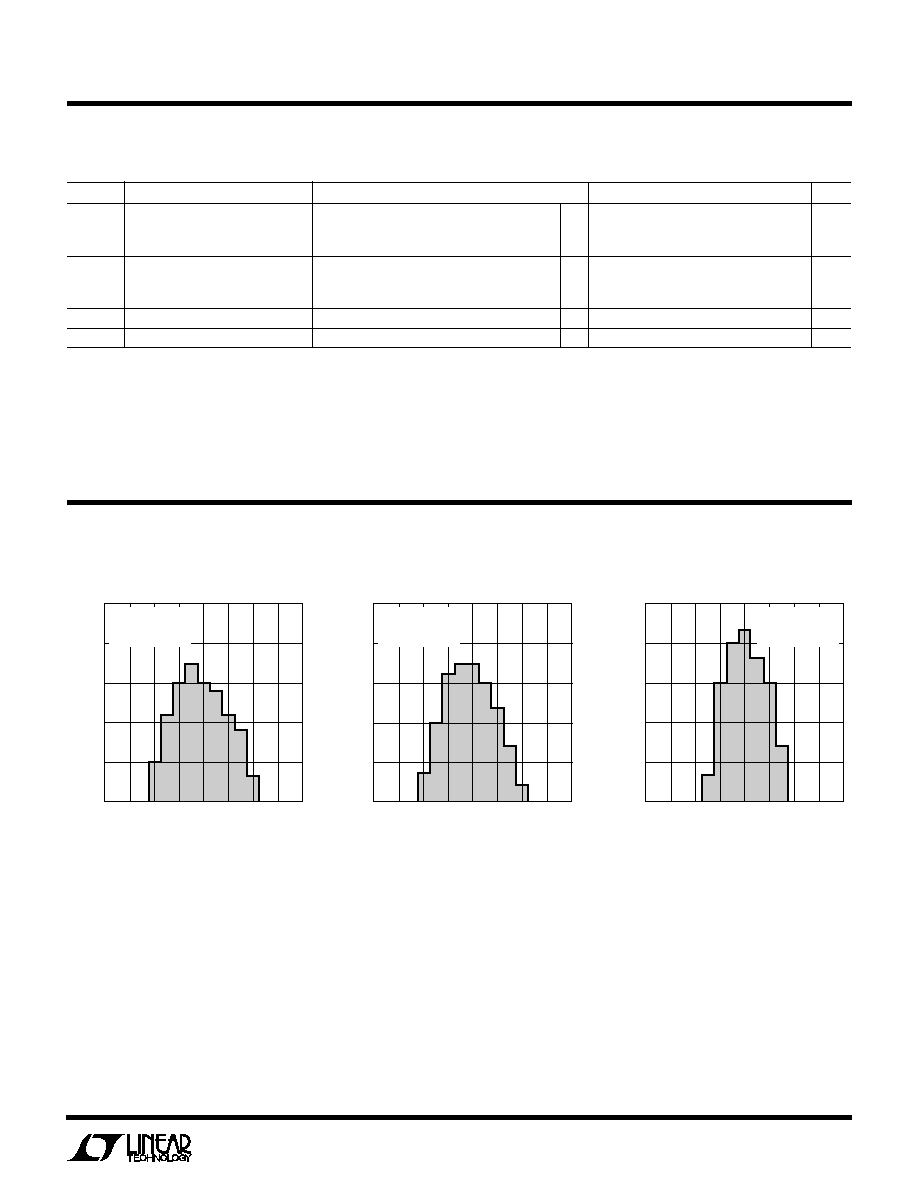
TYPICAL PERFOR
M
A
N
CE CHARACTERISTICS
U
W
INPUT OFFSET VOLTAGE (
µ
V)
400
PERCENT OF UNITS (%)
15
20
25
100
100
400
1466L/67L G01
10
5
0
300 200
0
200 300
V
S
= 5V, 0V
V
CM
= 0V
1900 AMPLIFIERS
V
OS
Distribution, V
CM
= 0V
INPUT OFFSET VOLTAGE SHIFT (
µ
V)
400
PERCENT OF UNITS (%)
15
20
25
100
100
400
1466L/67L G03
10
5
0
300 200
0
200 300
V
S
= 5V, 0V
V
CM
= 0V TO 5V
1900 AMPLIFIERS
INPUT OFFSET VOLTAGE (
µ
V)
400
PERCENT OF UNITS (%)
15
20
25
100
100
400
1466L/67L G02
10
5
0
300 200
0
200 300
V
S
= 5V, 0V
V
CM
= 5V
1900 AMPLIFIERS
V
OS
Distribution, V
CM
= 5V
V
OS
Shift, V
CM
= 0V to 5V