 | –≠–ª–µ–∫—Ç—Ä–æ–Ω–Ω—ã–π –∫–æ–º–ø–æ–Ω–µ–Ω—Ç: LT1470 | –°–∫–∞—á–∞—Ç—å:  PDF PDF  ZIP ZIP |
1
LTC1470/LTC1471
Single and Dual
PCMCIA Protected
3.3V/5V V
CC
Switches
FEATURES
s
Single 3.3V/5V Switch in 8-Pin SO Package
s
Dual 3.3V/5V Switch in 16-Pin SO Package
s
Built-In Current Limit and Thermal Shutdown
s
Built-In Charge Pumps (No 12V Required)
s
Extremely Low R
DS(ON)
MOSFET Switches
s
Output Current Capability: 1A
s
Inrush Current Limited (Drives 150
µ
F Loads)
s
Quiescent Current in Standby: 1
µ
A
s
No Parasitic Body Diodes
s
Built-In XOR Function Eliminates "Glue" Logic
s
Break-Before-Make Switching
s
Controlled Rise and Fall Times
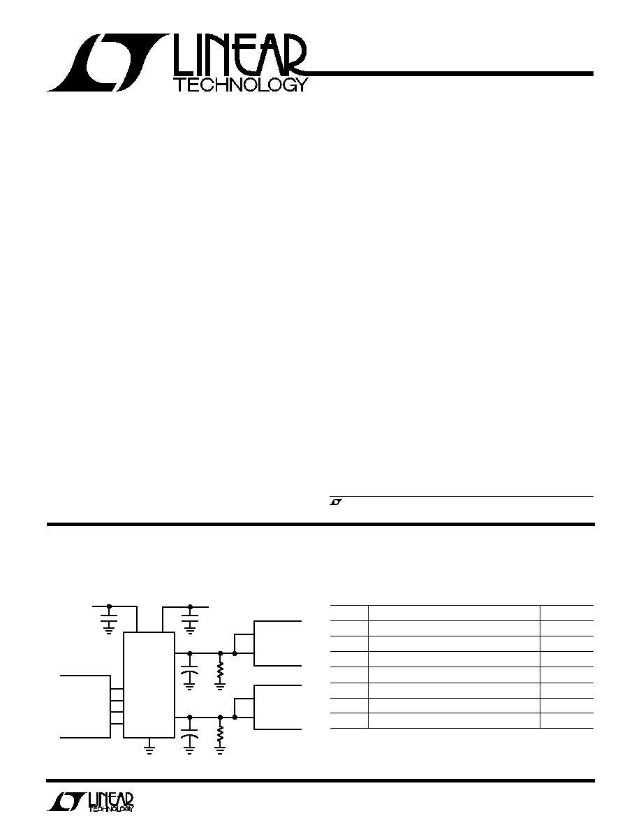
TYPICAL APPLICATIO
N
U
LTC1471
AEN1
AEN0
BEN1
BEN0
5V
IN
3V
IN
BOUT
AOUT
PCMCIA
CARD SLOT
CONTROLLER
GND
0.1
µ
F
5V
3.3V
0.1
µ
F
1470/71 TA01
PCMCIA
CARD SLOT
+
V
CC
V
CC
1
µ
F
10k
(Hi-Z/3.3V/5V)
PCMCIA
CARD SLOT
+
V
CC
V
CC
1
µ
F
10k
(Hi-Z/3.3V/5V)
The LTC
Æ
1470 switches the V
CC
pins of a Personal Com-
puter Memory Card International Association (PCMCIA)
card slot between three operating states: OFF, 3.3V and
5V. Two low R
DS(ON)
N-channel power MOSFETs are
driven by a built-in charge pump which generates a
voltage higher than the supply voltage to fully enhance
each switch when selected by the input control logic.
The LTC1470 inputs are compatible with industry stan-
dard PCMCIA controllers. A built-in XOR ensures that both
switches are never on at the same time. This function also
makes the LTC1470 compatible with both active-low and
active-high controllers (see Applications Information sec-
tion). The switch rise times are controlled to eliminate
power supply glitching.
The LTC1470 features built-in SafeSlot
TM
current limit and
thermal shutdown. The output is limited to 1A during short
circuit to ground but 2A of peak operating current is
allowed.
The LTC1471 is a dual version of the LTC1470 and is
available in a 16-pin SO package.
SafeSlot is a trademark of Linear Technology Corporation.
Dual Slot PCMCIA 3.3V/5V V
CC
Switch
Linear Technology PCMCIA Product Family
DESCRIPTIO
N
U
, LTC and LT are registered trademarks of Linear Technology Corporation.
DEVICE
DESCRIPTION
PACKAGE
LT
Æ
1312
Single PCMCIA VPP Driver/Regulator
8-Pin SO
LT1313
Dual PCMCIA VPP Driver/Regulator
16-Pin SO*
LTC1314
Single PCMCIA Switch Matrix
14-Pin SO
LTC1315
Dual PCMCIA Switch Matrix
24-Pin SSOP
LTC1470
Single Protected V
CC
3.3V/5V Switch Matrix
8-Pin SO
LTC1471
Dual Protected V
CC
3.3V/5V Switch Matrix
16-Pin SO*
LTC1472
Protected V
CC
and VPP Switch Matrix
16-Pin SO*
*Narrow Body
APPLICATIO
N
S
U
s
Notebook Computers
s
Palmtop Computers
s
Pen-Based Computers
s
Handi-Terminals
s
PC Card Reader/Writers
s
3.3V/5V Power Supply Switch
2
LTC1470/LTC1471
ABSOLUTE
M
AXI
M
U
M
RATINGS
W
W
W
U
3.3V Supply Voltage (Note 1) .................................. 7V
5V Supply Voltage (Note1) ....................................... 7V
Enable Input Voltage ........................ 7V to (GND ≠ 0.3V)
Output Voltage (OFF) (Note 1) ......... 7V to (GND ≠ 0.3V)
Output Short-Circuit Duration .......................... Indefinite
Operating Temperature ............................... 0
∞
C to 70
∞
C
Junction Temperature .......................................... 100
∞
C
Storage Temperature Range ................ ≠65
∞
C to 150
∞
C
Lead Temperature (Soldering, 10 sec) ................. 300
∞
C
PACKAGE/ORDER I
N
FOR
M
ATIO
N
W
U
U
ORDER PART
NUMBER
LTC1471CS
1470
S8 PART MARKING
ORDER PART
NUMBER
T
JMAX
= 100
∞
C,
JA
= 100
∞
C/W
Consult factory for Industrial and Military grade parts.
SYMBOL
PARAMETER
CONDITIONS
MIN
TYP
MAX
UNITS
3V
IN
3.3V Supply Voltage Range
2.70
3.60
V
5V
IN
5V Supply Voltage Range
4.75
5.25
V
I
3VIN
3.3V Supply Current
Program to Hi-Z (Note 3)
q
0.01
10
µ
A
Program to 3.3V, No Load (Note 3)
q
40
80
µ
A
Program to 5V, No Load (Note 3)
q
0.01
10
µ
A
I
5VIN
5V Supply Current
Program to Hi-Z (Note 3)
q
0.01
10
µ
A
Program to 3.3V (Note 3)
q
100
160
µ
A
Program to 5V (Note 3)
q
140
200
µ
A
R
ON
3.3V Switch ON Resistance
Program to 3.3V, I
OUT
= 500mA
0.12
0.16
5V Switch ON Resistance
Program to 5V, I
OUT
= 500mA
0.14
0.18
I
LKG
Output Leakage Current OFF
Program to Hi-Z, 0V
V
OUT
5V (Note 3)
q
±
10
µ
A
I
LIM3V
3.3V Current Limit
Program to 3.3V, V
OUT
= 0V (Note 4)
1
A
I
LIM5V
5V Current Limit
Program to 5V, V
OUT
= 0V (Note 4)
1
A
V
ENH
Enable Input High Voltage
q
2.0
V
V
ENL
Enable Input Low Voltage
q
0.8
V
I
EN
Enable Input Current
0V
V
EN
5V
q
±
1
µ
A
ELECTRICAL CHARACTERISTICS
3V
IN
= 3.3V, 5V
IN
= 5V (Note 2), T
A
= 25
∞
C, unless otherwise noted.
LTC1470CS8
T
JMAX
= 100
∞
C,
JA
= 150
∞
C/W
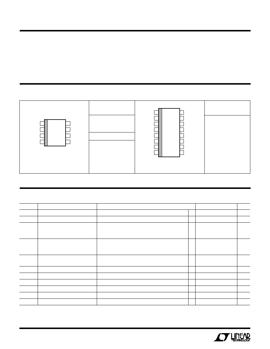
1
2
3
4
8
7
6
5
TOP VIEW
OUT
3V
IN
3V
IN
GND
OUT
5V
IN
EN1
EN0
S8 PACKAGE
8-LEAD PLASTIC SO
TOP VIEW
S PACKAGE
16-LEAD PLASTIC SO
1
2
3
4
5
6
7
8
16
15
14
13
12
11
10
9
AOUT
A5V
IN
AEN1
AEN0
GND
B3V
IN
B3V
IN
BOUT
AOUT
A3V
IN
A3V
IN
GND
BEN0
BEN1
B5V
IN
BOUT
3
LTC1470/LTC1471
ELECTRICAL CHARACTERISTICS
SYMBOL
PARAMETER
CONDITIONS
MIN
TYP
MAX
UNITS
t
0
to
t
3
Delay and Rise Time (Note 5)
Transition from 0V to 3.3V, R
OUT
= 100
, C
OUT
= 1
µ
F
0.2
0.32
1.0
ms
t
3
to
t
5
Delay and Rise Time (Note 5)
Transition from 3.3V to 5V, R
OUT
= 100
, C
OUT
= 1
µ
F
0.2
0.52
1.0
ms
t
0
to
t
5
Delay and Rise Time (Note 5)
Transition from 0V to 5V, R
OUT
= 100
, C
OUT
= 1
µ
F
0.2
0.38
1.0
ms
The
q
denotes the specifications which apply over the full operating
temperature range.
Note 1: For the LTC1470, the two output pins (1, 8) must be connected
together and the two 3.3V supply input pins (6 , 7) must be connected
together. For the LTC1471, the two AOUT pins (1, 16) must be connected
together, the two BOUT pins (8, 9) must be connected together, the two
A3V
IN
supply input pins (14, 15) must be connected together, the two
B3V
IN
supply pins (6, 7) must be connected together and the two GND
pins (5, 13) must be connected together.
Note 2: Power for the input logic and charge pump circuitry is derived
from the 5V
IN
supply pin(s) which must be continuously powered.
Note 3: Measured current is per channel with the other channel
programmed off for the LTC1471.
Note 4: The output is protected with foldback current limit which reduces
the short-circuit (0V) currents below peak permissible current levels at
higher output voltages.
Note 5: To 90% of final value.
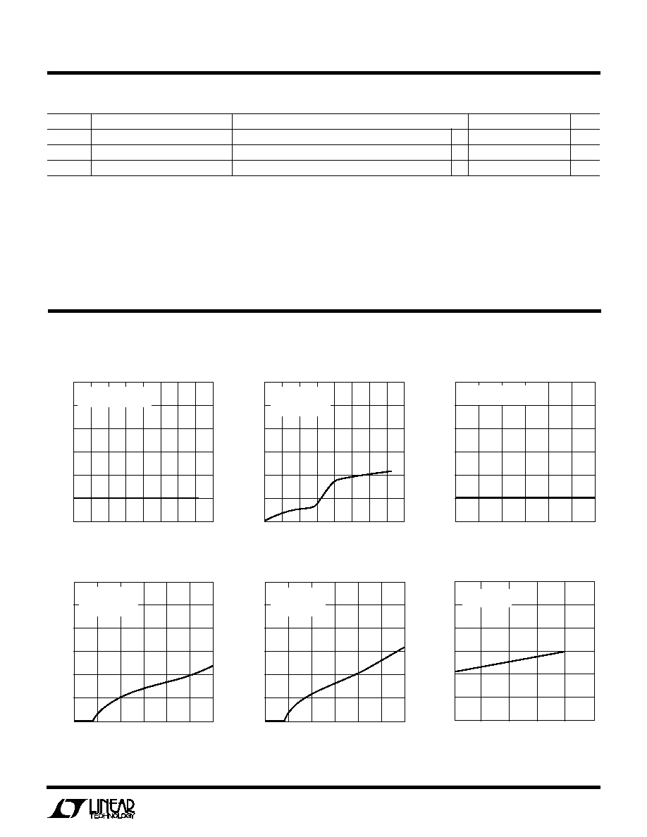
TYPICAL PERFOR
M
A
N
CE CHARACTERISTICS
U
W
3V
IN
= 3.3V, 5V
IN
= 5V (Note 2), T
A
= 25
∞
C, unless otherwise noted.
(LTC1470 or 1/2 LTC1471)
3V
IN
SUPPLY VOLTAGE (V)
0
0
3V
IN
SUPPLY CURRENT (
µ
A)
20
40
60
80
1
2
3
4
1470/71 G05
100
120
T
A
= 25
∞
C
PROGRAMMED TO
3.3V, NO LOAD
3V
IN
SUPPLY VOLTAGE (V)
0
≠1
3V
IN
SUPPLY CURRENT (
µ
A)
0
1
2
3
1
2
3
4
1470/71 G04
4
5
T
A
= 25
∞
C
PROGRAMMED TO OFF
3V
IN
Supply Current (3.3V ON)
3V
IN
Supply Current (OFF)
5V
IN
SUPPLY VOLTAGE (V)
0
≠1
5V
IN
SUPPLY CURRENT (
µ
A)
0
1
2
3
5
1
2
3
4
1470/71 G01
5
6
4
T
A
= 25
∞
C
PROGRAMMED TO OFF
5V
IN
Supply Current (OFF)
JUNCTION TEMPERATURE (
∞
C)
0
0
3.3V SWITCH RESISTANCE (
)
0.05
0.10
0.15
0.20
0.25
0.30
25
50
75
100
1470/71 G07
125
PROGRAMMED
TO 3.3V
3.3V Switch Resistance
5V
IN
SUPPLY VOLTAGE (V)
0
0
5V
IN
SUPPLY CURRENT (
µ
A)
50
100
150
200
300
1
2
3
4
1470/71 G03
5
6
250
T
A
= 25
∞
C
PROGRAMMED
TO 3.3V, NO LOAD
5V
IN
Supply Current (3.3V ON)
5V
IN
Supply Current (5V ON)
5V
IN
SUPPLY VOLTAGE (V)
0
0
5V
IN
SUPPLY CURRENT (
µ
A)
50
100
150
200
300
1
2
3
4
1470/71 G02
5
6
250
T
A
= 25
∞
C
PROGRAMMED
TO 5V, NO LOAD
4
LTC1470/LTC1471
TYPICAL PERFOR
M
A
N
CE CHARACTERISTICS
U
W
PI
N
FU
N
CTIO
N
S
U
U
U
LTC1470
OUT (Pins 1, 8): Output Pins. The outputs of the LTC1470
are switched between three operating states: OFF, 3.3V
and 5V. These pins are protected against accidental short
circuits to ground by SafeSlot current limit circuitry which
protects the socket, the card, and the system power
supplies against damage. A second level of protection is
provided by thermal shutdown circuitry which protects
both switches against over-temperature conditions.
5V
IN
(Pin 2): 5V
Input Supply Pin. The 5V
IN
supply pin
serves two purposes. The first purpose is as the power
supply input for the 5V NMOS switch. The second purpose
is to provide power for the input, gate drive, and protection
circuitry for both the 3.3V and 5V V
CC
switches. This pin
must therefore be continuously powered.
EN1, EN0 (Pins 3, 4): Enable Inputs. The two V
CC
Enable
inputs are designed to interface directly with industry
standard PCMCIA controllers and are high impedance
CMOS gates with ESD protection diodes to ground, and
should not be forced below ground. Both inputs have
about 100mV of built-in hysteresis to ensure clean switch-
ing between operating modes. The LTC1470 is designed
to operate
without 12V power. The gates of the V
CC
NMOS
switches are powered by charge pumps from the 5V
IN
supply pins (see Applications Information section for
more detail). The Enable inputs should be turned off (both
asserted high or both asserted low) at least 100
µ
s before
the 5V
IN
power is removed to ensure that both V
CC
NMOS
switch gates are fully discharged and both switches are in
the high impedance mode.
GND (Pin 5): Ground Connection.
3V
IN
(Pins 6, 7): 3V
Input Supply Pins. The 3V
IN
supply
pins serve as the power supply input for the 3.3V switches.
These pins do not provide any power to the internal control
circuitry and therefore do not consume any power when
unloaded or turned off.
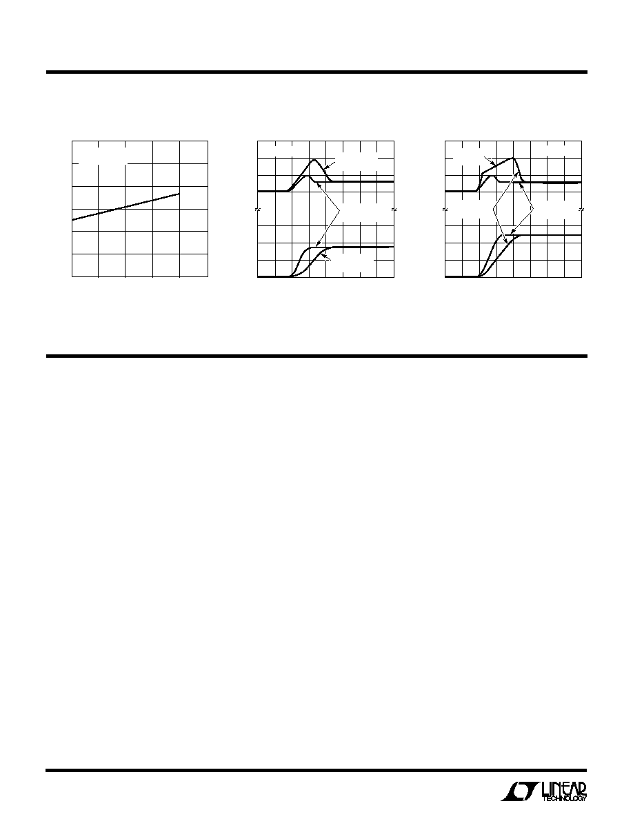
JUNCTION TEMPERATURE (
∞
C)
0
0
5V SWITCH RESISTANCE (
)
0.05
0.10
0.15
0.20
0.25
0.30
25
50
75
100
1470/71 G06
125
PROGRAMMED
TO 5V
5V Switch Resistance
TIME (ms)
≠ 0.2
INRUSH CURRENT (A)
OUTPUT VOLTAGE (V)
0
1
1.4
1470/71 G08
6
4
0
0.2
0.6
1.0
2
3
2
0
0.4
0.8
1.2
C
OUT
= 15
µ
F
R
OUT
= 10
T
J
= 25
∞
C
CURRENT
LIMITED
C
OUT
= 150
µ
F
R
OUT
= 10
Inrush Current (5V Switch)
Inrush Current (3.3V Switch)
TIME (ms)
≠ 0.2
INRUSH CURRENT (A)
OUTPUT VOLTAGE (V)
0
1
1.4
1470/71 G09
6
4
0
0.2
0.6
1.0
2
3
2
0
0.4
0.8
1.2
T
J
= 25
∞
C
C
OUT
= 15
µ
F
R
OUT
= 6.6
C
OUT
= 150
µ
F
R
OUT
= 6.6
C
OUT
= 150
µ
F
R
OUT
= 6.6
(LTC1470 or 1/2 LTC1471)
5
LTC1470/LTC1471
PI
N
FU
N
CTIO
N
S
U
U
U
TTL-TO-CMOS
CONVERTER
OSCILLATOR
AND BIAS
GATE CHARGE
AND
DISCHARGE
CONTROL LOGIC
CHARGE
PUMP
GATE CHARGE
AND
DISCHARGE
CONTROL LOGIC
CURRENT LIMIT
AND THERMAL
SHUTDOWN
5V
IN
0.14
0.12
OUTPUT
3V
IN
BREAK-BEFORE-
MAKE SWITCH
AND CONTROL
TTL-TO-CMOS
CONVERTER
EN0
EN1
LTC1470-BD01
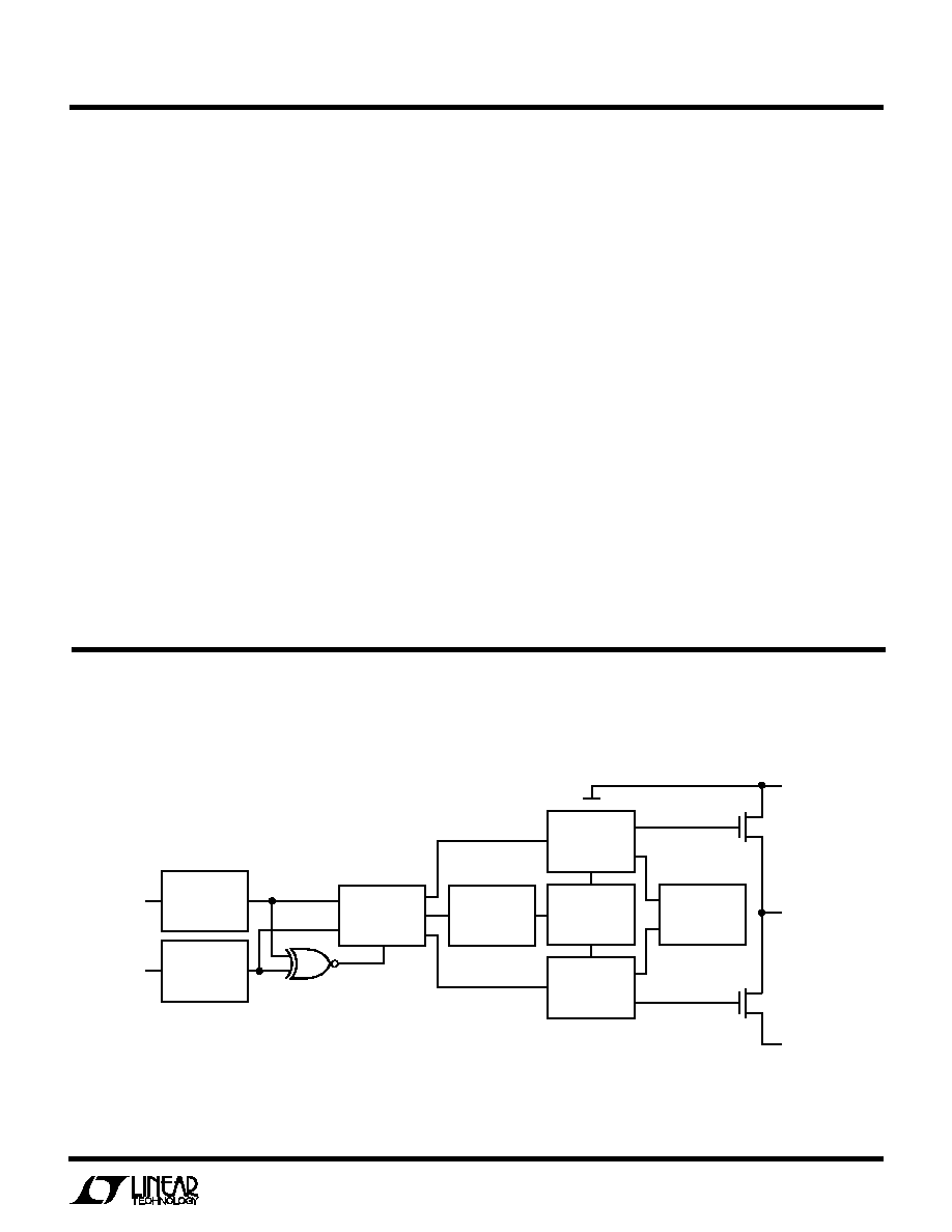
BLOCK DIAGRA
M
W
LTC1471
AOUT, BOUT(Pins 1, 16, 8, 9): Output Pins. The outputs
of the LTC1471 are switched between three operating
states: OFF, 3.3V and 5V. These pins are protected against
accidental short circuits to ground by SafeSlot current
limit circuitry which protects the socket, the card, and the
system power supplies against damage. A second level of
protection is provided by thermal shutdown circuitry.
5V
IN
(Pins 2, 10): 5V
Input Supply Pins. The 5V
IN
supply
pins serve two purposes. The first purpose is as the power
supply input for the 5V NMOS switches. The second
purpose is to provide power for the input, gate drive, and
protection circuitry. These pins must therefore be con-
tinuously powered.
EN1, EN0 (Pins 3, 4, 11, 12): Enable Inputs. The enable
inputs are designed to interface directly with industry
standard PCMCIA controllers and are high impedance
CMOS gates with ESD protection diodes to ground, and
should not be forced below ground. All four inputs have
about 100mV of built-in hysteresis to ensure clean switch-
ing between operating modes. The LTC1471 is designed
to operate
without 12V power. The gates of the V
CC
NMOS
switches are powered by charge pumps from the 5V
IN
supply pins (see Applications Information section for
more detail). The enable inputs should be turned off at
least 100
µ
s before the 5V
IN
power is removed to ensure
that all NMOS switch gates are fully discharged and are in
the high impedance mode.
GND (Pins 5, 13): Ground Connections.
3V
IN
(Pins 6, 7, 14, 15): 3V
Input Supply Pins. The 3V
IN
supply pins serve as the power supply input for the 3.3V
switches. These pins do not not provide any power to the
internal control circuitry, and therefore, do not consume
any power when unloaded or turned off.
(LTC1470 or 1/2 LTC1471)
6
LTC1470/LTC1471
OPERATIO
N
U
The LTC1470 (or 1/2 of the LTC1471) consists of the
following functional blocks:
Input TTL/CMOS Converters
The enable inputs are designed to accommodate a wide
range of 3V and 5V logic families. The input threshold
voltage is approximately 1.4V with approximately 100mV
of hysteresis. The inputs enable the bias generator, the
gate charge pumps and the protection circuity which are
powered from the 5V supply. Therefore, when the inputs
are turned off, the entire circuit is powered down and the
5V
supply current drops below 1
µ
A.
XOR Input Circuitry
By employing an XOR function, which locks out the 3.3V
switch when the 5V switch is turned on and locks out the
5V switch when the 3.3V switch is turned on, there is no
danger of both switches being on at the same time. This
XOR function also makes it possible to work with either
active -low or active-high PCMCIA V
CC
switch control logic
(see Applications Information section for further details).
Break-Before-Make Switch Control
Built-in delays are provided to ensure that the 3.3V and 5V
switches are non-overlapping. Further, the gate charge
pump includes circuitry which ramps the NMOS switches
on slowly (400
µ
s typical rise time) but turns them off
much more quickly (typically 10
µ
s).
Bias, Oscillator and Gate Charge Pump
When either the 3.3V or 5V switch is enabled, a bias
current generator and high frequency oscillator are turned
on. The on-chip capacitive charge pump generates ap-
proximately 12V of gate drive for the internal low R
DS(ON)
NMOS V
CC
switches from the 5V
IN
power supply. There-
fore, an external 12V supply is not required to switch the
V
CC
output. The 5V
IN
supply current drops below 1
µ
A
when both switches are turned off.
Gate Charge and Discharge Control
All switches are designed to ramp on slowly (400
µ
s typical
rise time). Turn-off time is much quicker (typically 10
µ
s).
To ensure that both V
CC
NMOS switch gates are fully
discharged, program the switch to the high impedance
mode at least 100
µ
s before turning off the 5V power
supply.
Switch Protection
Both switches are protected against accidental short cir-
cuits with SafeSlot foldback current limit circuits which
limit the output current to typically 1A when the output is
shorted to ground. Both switches also have thermal shut-
down which limits the power dissipation to safe levels.
APPLICATIO
N
S I
N
FOR
M
ATIO
N
W
U
U
U
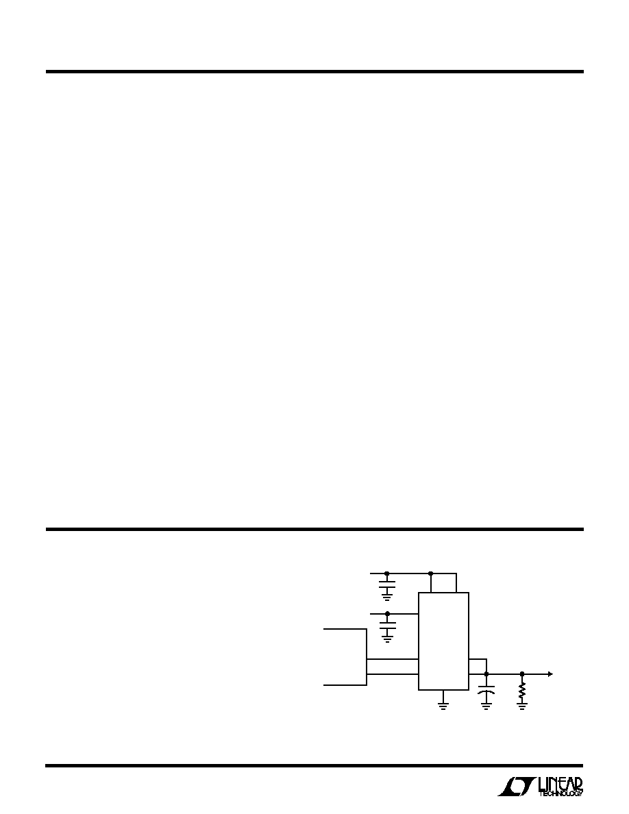
Figure 1. Direct Interface to CL-PD6710 PCMCIA Controller
LTC1470
EN0
EN1
3V
IN
5V
IN
3V
IN
OUT
OUT
GND
+
3.3V
5V
0.1
µ
F
0.1
µ
F
1
µ
F
TANT
10k
(OFF/3.3V/5V)
TO CARD
V
CC
PINS
CL-PD6710
V
CC
_5
V
CC
_3
1470/71 F01
The LTC1470/LTC1471 are designed to interface directly
with industry standard PCMCIA card controllers.
Interfacing with the CL-PD6710
Figure 1 is a schematic diagram showing the LTC1470
interfaced with a standard PCMCIA slot controller. The
LTC1470 accepts logic control directly from the CL-PD6710.
The XOR input function allows the LTC1470 to interface
directly to the active-low V
CC
control outputs of the CL-
PD6710 for 3.3V/5V voltage selection (see the following
Switch Truth Table). Therefore, no "glue" logic is required
to interface to this PCMCIA compatible card controller.
7
LTC1470/LTC1471
Supply Bypassing
For best results bypass the supply input pins with 1
µ
F
capacitors as close as possible to the LTC1470. Some-
times much larger capacitors are already available at the
outputs of the 3.3V and 5V power supply. In this case it is
still good practice to use 0.1
µ
F capacitors as close as
possible to the device, especially if the power supply
output capacitors are more than 2" away on the printed
circuit board.
Output Capacitors and Pull-Down Resistor
The output pin is designed to ramp on slowly, typically
400
µ
s rise time. Therefore, capacitors as large as 150
µ
F
can be driven without producing voltage spikes on the
3V
IN
or 5V
IN
supply pins (see graphs in Typical Perfor-
mance Characteristics section). The output pin should
have a 0.1
µ
F to 1
µ
F capacitor for noise reduction and
smoothing.
A 10k pull-down resistor is recommended at the output to
ensure that the output capacitor is fully discharged when the
output is switched OFF. This resistor also ensures that the
output is discharged between the 3.3V and 5V transition.
Supply Sequencing
Because the 5V supply is the source of power for both of the
switch control circuits, it is best to sequence the power
supplies such that the 5V supply is powered before, or
simultaneous to, the application of 3.3V.
It is interesting to note, however, that the switches are NMOS
transistors which require charge pumps to generate gate
voltages higher than the supply rails for full enhancement.
Because the gate voltages start at 0V when the supplies are
first activated, the switches always start in the off state and
do not produce glitches at the outputs when powered.
If the 5V supply must be turned off, it is important to program
all switches to the Hi-Z or 0V state at least 100
µ
s before the
5V power is removed to ensure that the NMOS switch gates
are fully discharged to 0V. Whenever possible, however, it is
best to leave the 5V
IN
pin(s) continuously powered. The
LTC1470/LTC1471 quiescent current drops to <1
µ
A with all
the switches turned off and therefore no 5V power is
consumed in the standby mode.
APPLICATIO
N
S I
N
FOR
M
ATIO
N
W
U
U
U
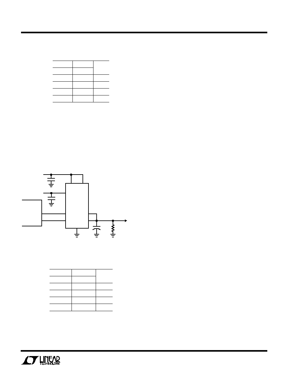
A_V
CC
_3
A_V
CC
_5
EN0
EN1
OUT
0
0
Hi-Z
0
1
3.3V
1
0
5V
1
1
Hi-Z
Truth Table for CL-PD6710 Controller
Interfacing with "365" Type Controllers
The LTC1470 also interfaces directly with "365" type
controllers as shown in Figure 2. Note that the V
CC
Enable
inputs are connected differently than to the CL-PD6710
controller because the "365" type controllers use active-
high logic control of the V
CC
switches (see the following
Switch Truth Table). No "glue" logic is required to inter-
face to this type of PCMCIA compatible controller.
LTC1470
EN0
EN1
3V
IN
5V
IN
3V
IN
OUT
OUT
GND
+
3.3V
5V
0.1
µ
F
0.1
µ
F
1
µ
F
TANT
10k
(OFF/3.3V/5V)
TO CARD
V
CC
PINS
"365" TYPE
CONTROLLER
1470/71 F02
A_V
CC
_EN0
A_V
CC
_EN1
Figure 2. Direct Interface with "365" Type PCMCIA Controller
Truth Table for "365" Type Controller
A_V
CC
_EN0
A_V
CC
_EN1
EN0
EN1
OUT
0
0
Hi-Z
0
1
3.3V
1
0
5V
1
1
Hi-Z
8
LTC1470/LTC1471
APPLICATIO
N
S I
N
FOR
M
ATIO
N
W
U
U
U
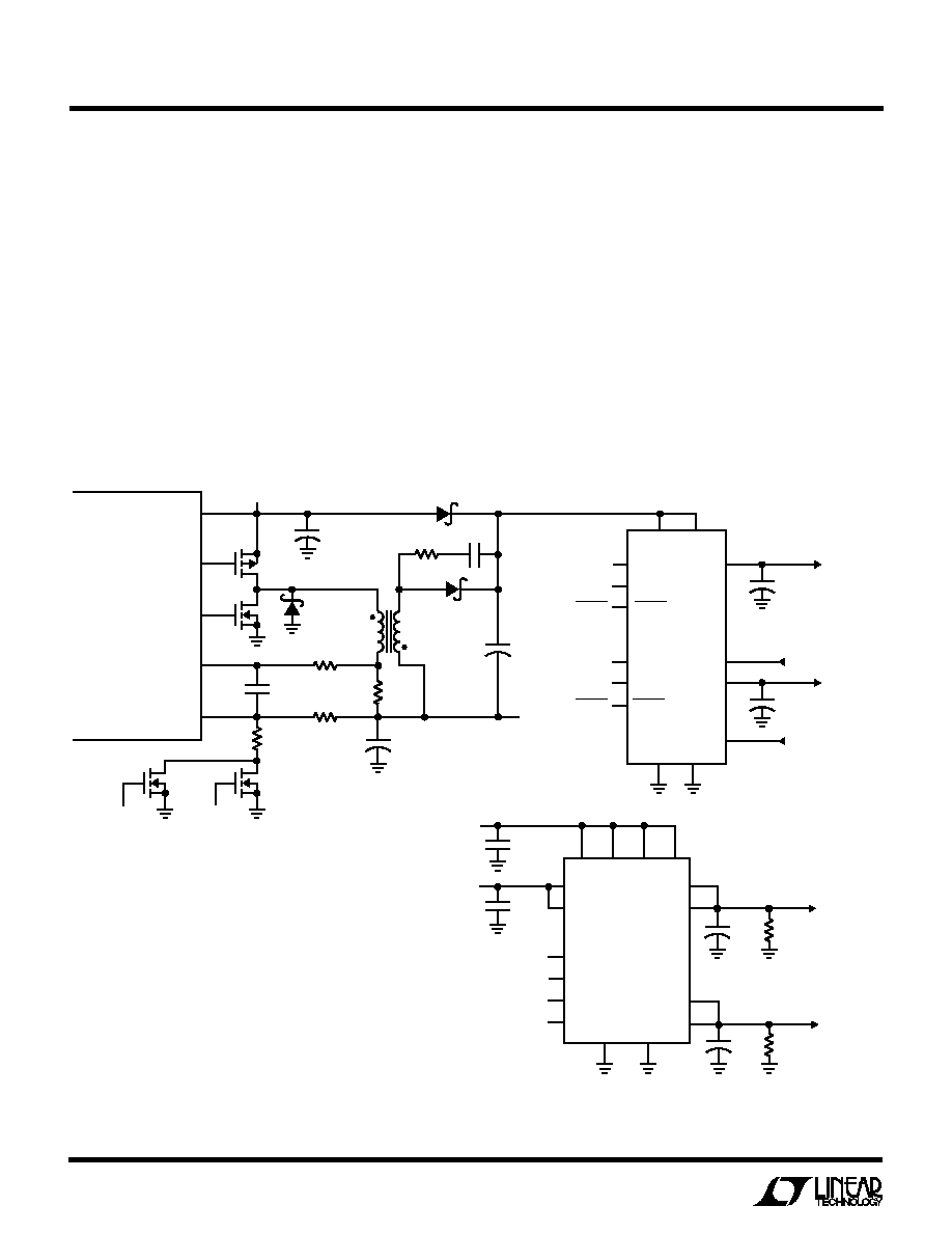
TOTAL SYSTEM COST CONSIDERATIONS
The cost of an additional step-up switching regulator, induc-
tor, rectifier and capacitors to produce 12V for VPP can be
eliminated by using an auxiliary winding on either the 3.3V
or 5V output of the system switching regulator to produce an
auxiliary 15V supply for VPP power.
And, because the LTC1470/LTC1471 do not require 12V
power to operate (only 5V), the 12V VPP regulation and
switching may be operated separately from the 3.3V/5V V
CC
switching. This increases system configuration flexibility
and
reduces total system cost by eliminating the need for a
third regulator for 12V power.
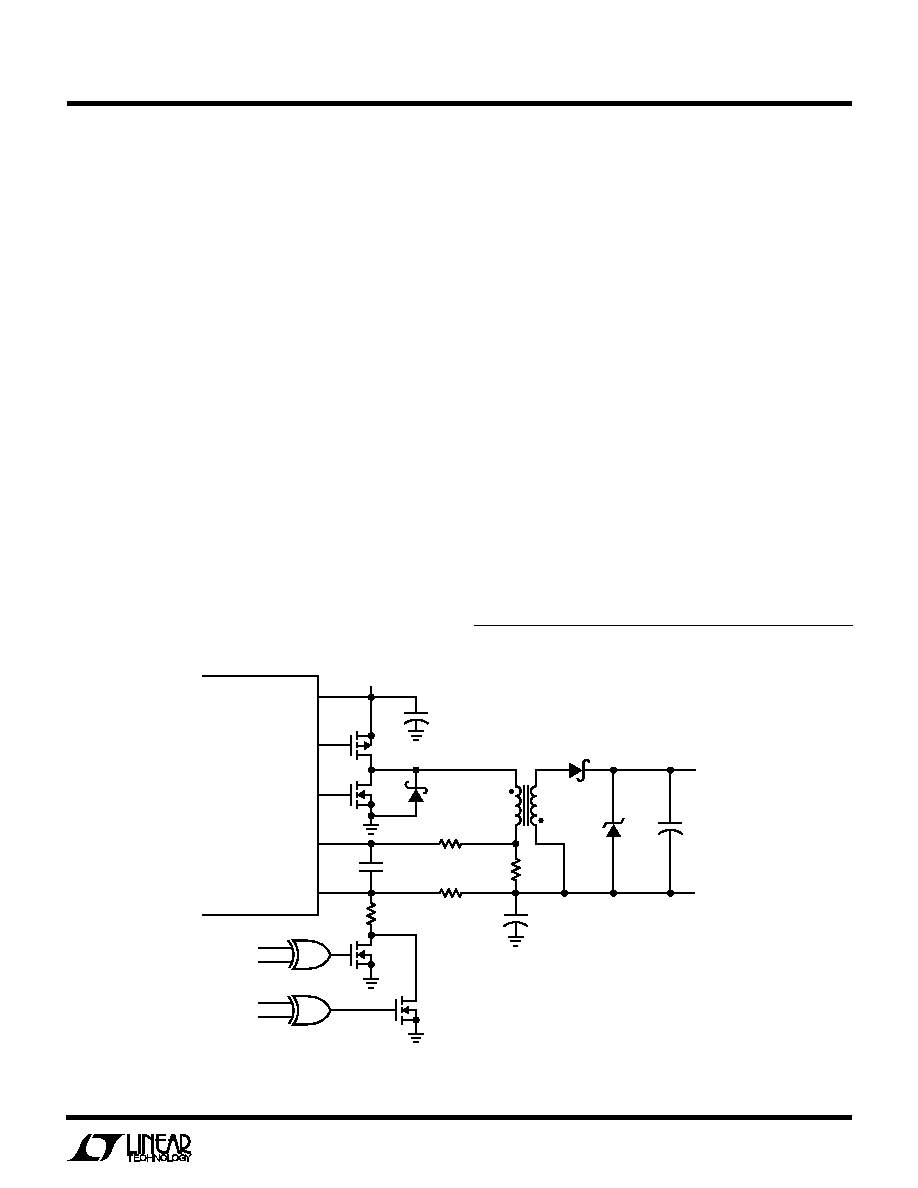
LTC1142HV Auxiliary Winding Power Supply
Figure 3 is a schematic diagram which describes how a
loosely regulated 15V power supply is created by adding an
auxiliary winding to the 5V inductor in a split 3.3V/5V
LTC1142HV power supply system. An LT1313, dual VPP
regulator/driver with SafeSlot protection, produces "clean"
3.3V, 5V and 12V power from this loosely regulated 15V
output for the PC card slot VPP pins. (See LT1312 and
LT1313 data sheets for further detail.)
A turns ratio of 1:1.8 is used for transformer T1 to ensure that
the input voltage to the LT1313 falls between 13V and 20V
under all load conditions. The 9V output from this additional
Figure 3. Cost Effective Complete SafeSlot Dual PCMCIA Power Management System
(with 15V Auxiliary Supply from LTC1142HV 5V Regulator Inductor)
+
10
9
20
15
14
BVPPEN0
Q4
2N7002
R3
18k
C2
1000pF
C1
68
µ
F
C3
220
µ
F
C5
22
µ
F
1
µ
F
0.1
µ
F
10k
0.1
µ
F
1
µ
F
1
µ
F
TANT
1
µ
F
TANT
V
S
A3V
IN
A3V
IN
LTC1471
B3V
IN
B3V
IN
(15V)
V
S
5V
OUTPUT
3.3V
5V
T1*
30
µ
H
* LPE-6562-A026 DALE (605) 665-9301
R5
0.033
Q1
Q2
R1
100
R4
22
C4
1000pF
D2
MBRS140
D3
MBRS130T3
D1
MBRS140
1.8:1
V
IN
6.5V TO 18V
Q3
2N7002
AVPPEN0
R2
100
+
+
+
AVPPEN0
AVPPEN1
AVALID
AEN0
AEN1
AVALID
BVPPEN0
BVPPEN1
BVALID
AV
CC
EN0
AV
CC
EN1
BV
CC
EN0
BV
CC
EN1
AEN0
AEN1
BEN0
BEN1
AOUT
AOUT
BOUT
BOUT
A5V
IN
B5V
IN
BEN0
BEN1
BVALID
ASENSE
BVPP
OUT
AVPP
OUT
BSENSE
FROM "A" V
CC
PINS
FROM "B" V
CC
PINS
TO "A" SLOT
VPP PINS
TO "A" SLOT
V
CC
PINS
TO "B" SLOT
VPP PINS
LT1313
GND
GND
1470/71 F03
GND
GND
+
TO "B" SLOT
V
CC
PINS
+
+
10k
V
IN
PDRIVE
NDRIVE
SENSE
+
SENSE
≠
1/2 LTC1142HV
(5V REG)
9
LTC1470/LTC1471
APPLICATIO
N
S I
N
FOR
M
ATIO
N
W
U
U
U
winding is rectified by diode D2, added to the main 5V output
and applied to the input of the LT1313. (Note that the
auxiliary winding must be phased properly as shown in
Figure 3.)
When the 12V output is activated by a TTL high on either VPP
enable lines, the 5V section of the LTC1142HV is forced into
continuous mode operation. A resistor divider composed of
R2, R3 and switch Q3 forces an offset which is subtracted
from the internal offset at the Sense
≠
input (pin 14) of the
LTC1142HV. When this external offset cancels the built-in
25mV offset, Burst Mode
TM
operation is inhibited and the
LTC1142HV is forced into continuous mode operation. (See
LTC1142HV data sheet for further detail.) In this mode, the
15V auxiliary supply can be loaded without regard to the
loading on the 5V output of the LTC1142HV.
Continuous mode operation is only invoked when the LT1313
is programmed to 12V. If the LT1313 is programmed to 0V,
3.3V or 5V, power is obtained directly from the main power
source (battery pack) through diode D1. Again, the LT1313
output can be loaded without regard to the loading of the
main 5V output.
R4 and C4 absorb transient voltage spikes associated with
the leakage inductance inherent in T1's secondary winding
and ensure that the auxiliary supply does not exceed 20V.
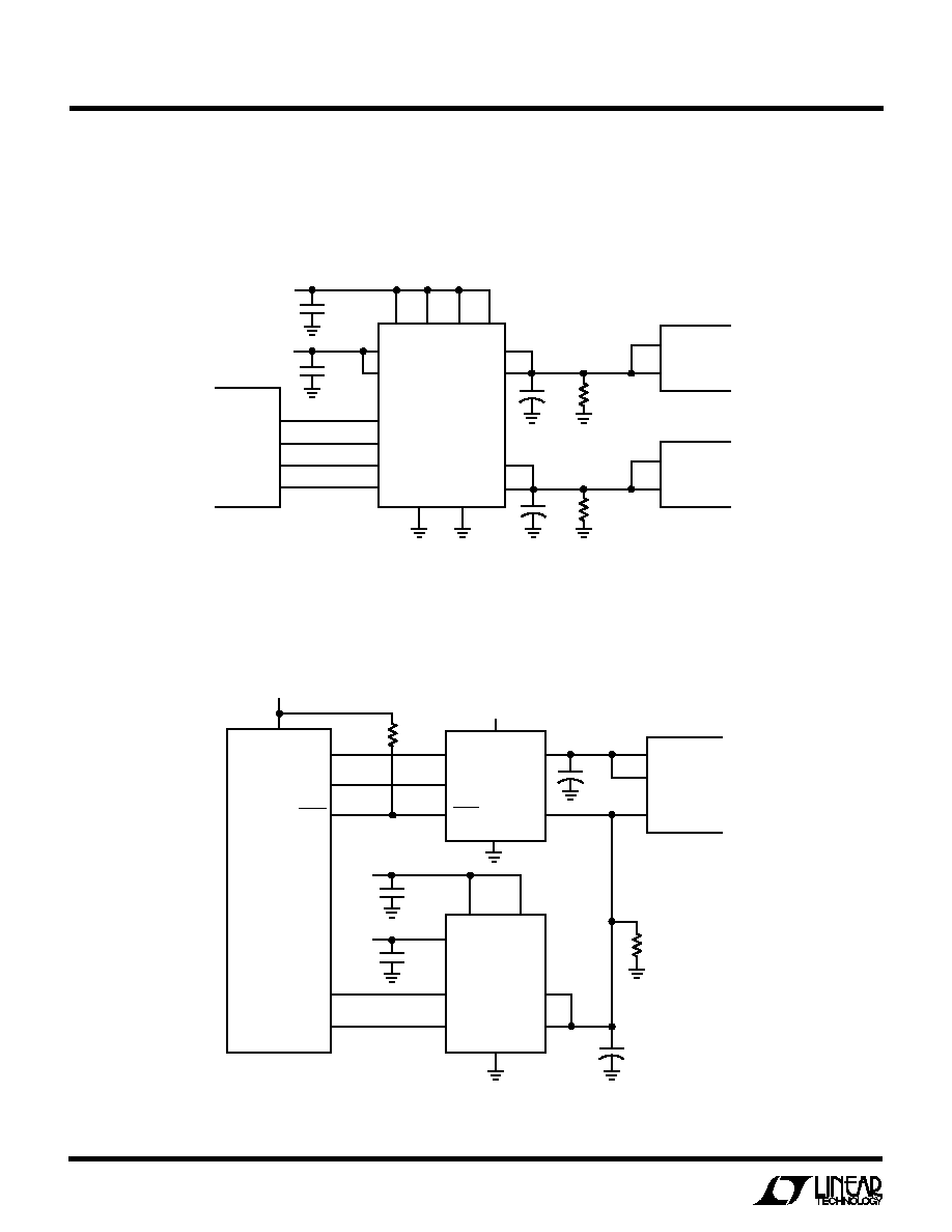
Auxiliary Power from the LTC1142 3.3V Output
For low-battery count applications (< 6.5V) it is necessary to
modify the circuit of Figure 3. As the input voltage falls, the
5V duty cycle increases to the point where there is simply not
enough time to transfer energy from the 5V primary winding
to the auxiliary winding. For applications where 12V load
currents exist in conjunction with these low input voltages,
use the circuit shown in Figure 4. In this circuit, the auxiliary
15V supply is generated from an overwinding on the 3.3V
inductor of the LTC1142 regulator output.
In Figure 3, power is drawn directly from the batteries
through D1 when the regulator is in Burst Mode operation
and the VPP pins require 3.3V or 5V. In this circuit, however,
Q3 and Q4 force the LTC1142 3.3V regulator into continuous
mode operation whenever 3.3V, 5V or 12V is programmed
at the VPP
OUT
pins of the LT1313. (See the LT1312 and
LT1313 data sheets for further detail.)
Figure 4. Deriving 15V from the 3.3V Output of the LTC1142 for VPP Power
Burst Mode is a trademark of Linear Technology Corporation.
24
23
6
1
28
R3
12k
AENVPP0
AENVPP1
C2
1000pF
C1
68
µ
F
C5
68
µ
F
C3
220
µ
F
D3
MBRS130T3
D2
MBRS1100
3.3V
OUTPUT
15V AUX
SUPPLY
T1*
15
µ
H
*CTX02-12753
COILTRONICS (407) 241-7876
R4
0.033
D4
18V
Q1
Q2
Q3
2N7002
Q4
2N7002
R1
100
3.37:1
V
IN
5.4V TO 11V
R2
100
+
+
1470/71 F04
+
V
IN
PDRIVE
NDRIVE
SENSE
+
SENSE
≠
1/2 LTC1142
(3.3V REG)
BENVPP0
BENVPP1
HC86
HC86
10
LTC1470/LTC1471
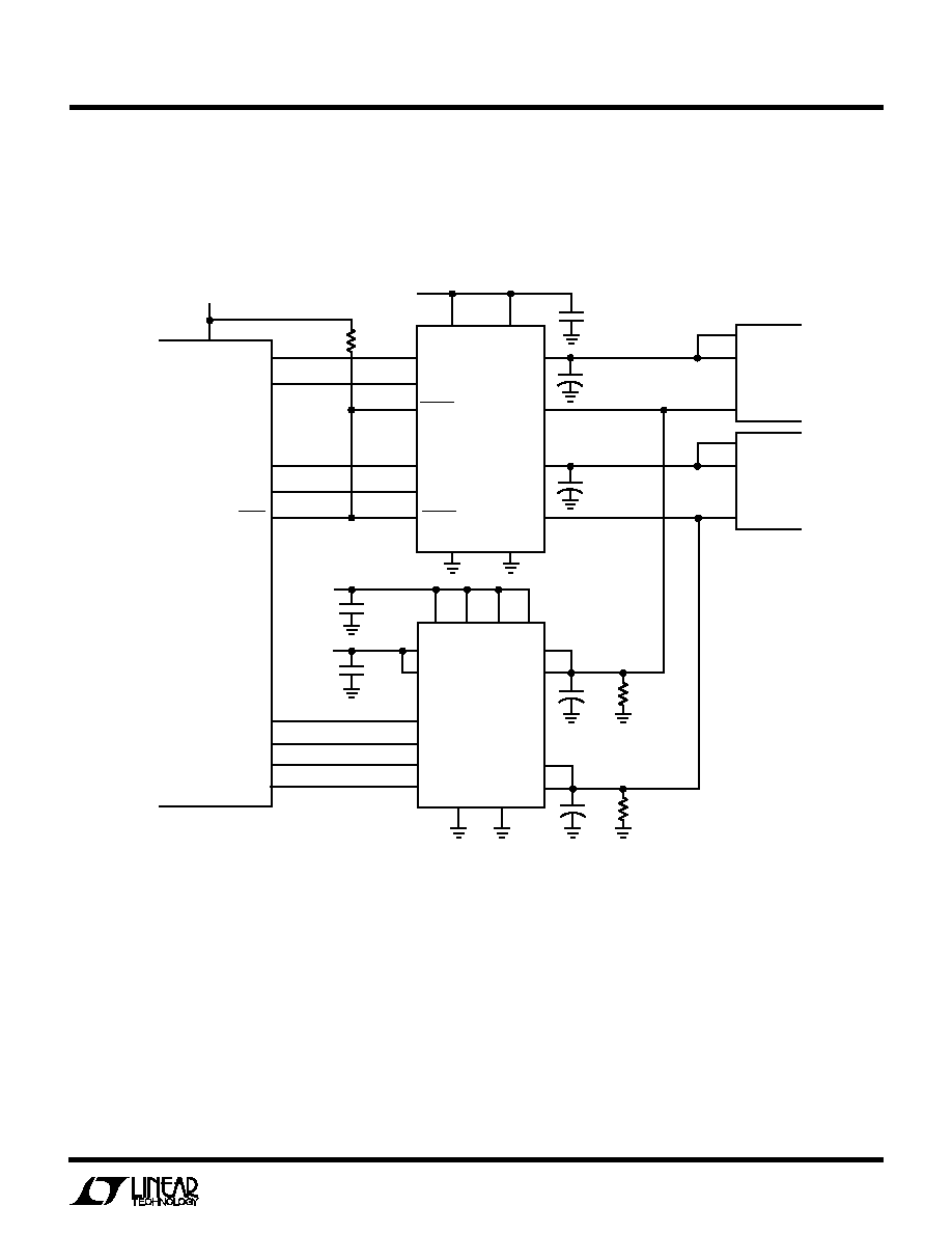
Dual Slot 3.3V/5V PCMCIA Controller with SafeSlot Current Limit
(Systems with No 12V Power Requirements)
0.1
µ
F
10k
0.1
µ
F
1
µ
F
TANT
1
µ
F
TANT
A3V
IN
A3V
IN
LTC1471
B3V
IN
B3V
IN
3.3V
5V
AEN0
AEN1
BEN0
BEN1
AOUT
AOUT
BOUT
BOUT
A5V
IN
B5V
IN
GND
1470/71 TA02
GND
(OFF/3.3V/5V)
(OFF/3.3V/5V)
+
+
10k
PCMCIA
CARD SLOT
V
CC
V
CC
PCMCIA
CARD SLOT
V
CC
V
CC
CL-PD6710
A_V
CC
_3
A_V
CC
_5
B_V
CC
_3
B_V
CC
_5
Single Slot PCMCIA Controller with SafeSlot Current Limit
Protection Using LT1312 Single VPP Regulator/Driver
LT1312
V
S
EN0
VALID
EN1
GND
1470/71 TA03
VPP
OUT
SENSE
LTC1470
3V
IN
3V
IN
5V
IN
EN0
GND
0UT
V
CC
0UT
+
+
1
µ
F
0.1
µ
F
0.1
µ
F
EN1
* FROM OVERWINDING ON 3.3V OR 5V INDUCTOR IN SYSTEM POWER SUPPLY.
SEE FIGURES 3, 4 FOR FURTHER DETAIL
VPP1
VPP2
PCMCIA
CARD SLOT
10k
1
µ
F
TANT
3.3V
5V
V
LOGIC
13V TO 20V*
51k
VPP_PGM
VPP_V
CC
VPP_VALID
V
CC
_5
CIRRUS LOGIC
CL-PD6710
V
CC
V
CC
_3
TYPICAL APPLICATIO
N
S
U
11
LTC1470/LTC1471
TYPICAL APPLICATIO
N
S
U
Information furnished by Linear Technology Corporation is believed to be accurate and reliable.
However, no responsibility is assumed for its use. Linear Technology Corporation makes no represen-
tation that the interconnection of circuits as described herein will not infringe on existing patent rights.
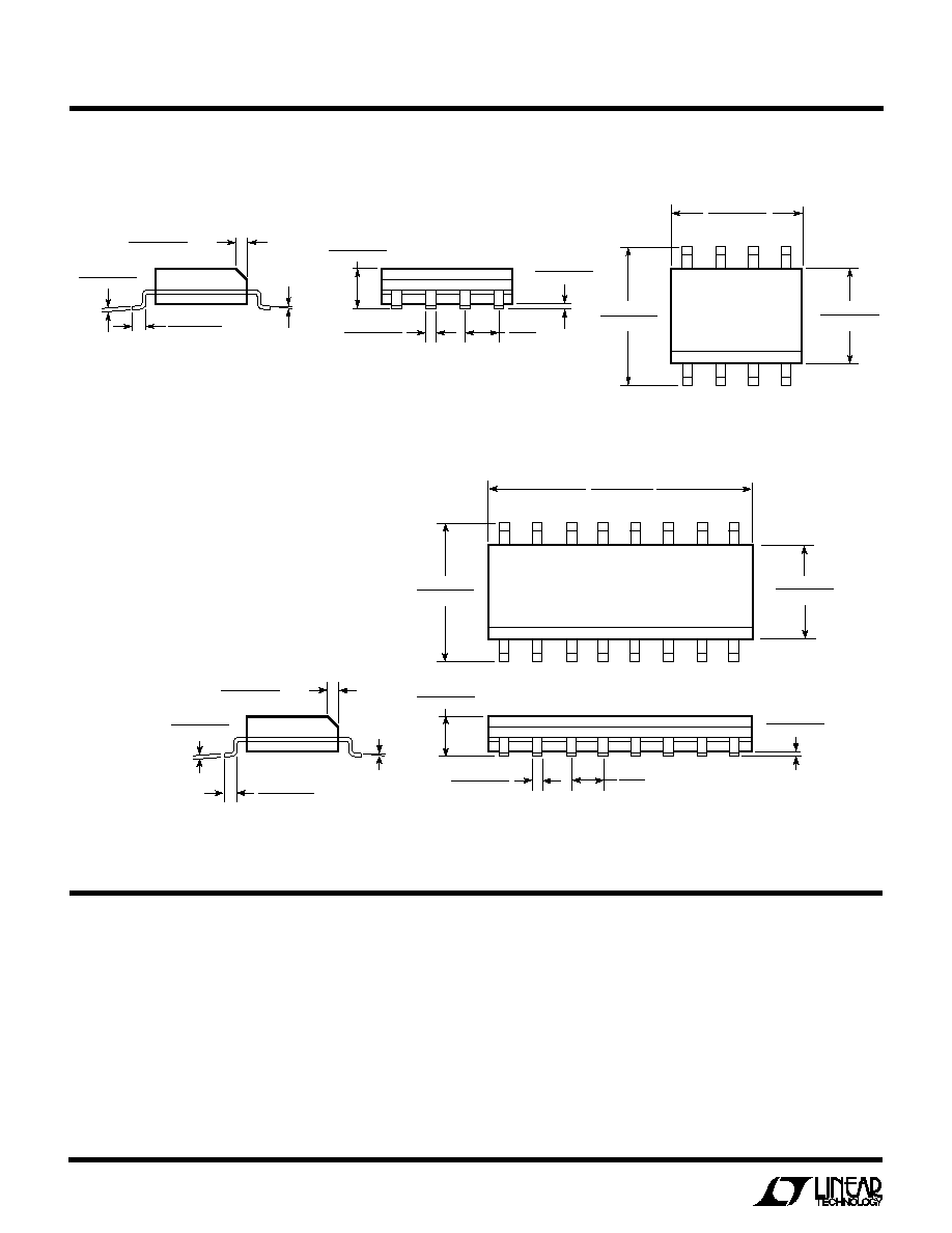
LT1313
BVALID
BEN1
AEN1
BEN0
AV
S
BV
S
AVPP
OUT
BVPP
OUT
GND
GND
13V TO 20V*
0.1
µ
F
1
µ
F
1
µ
F
VPP1
VPP2
VPP1
V
CC
V
CC
VPP2
PCMCIA
CARD SLOT
#1
PCMCIA
CARD SLOT
#2
A_VPP_PGM
A_VPP_V
CC
B_VPP_PGM
B_VPP_V
CC
VPP_VALID
A_V
CC
_3V
A_V
CC
_5V
B_V
CC
_3V
B_V
CC
_5V
1470/71 TA04
BSENSE
ASENSE
AEN0
AVALID
+
+
CL-PD6720
51k
V
LOGIC
PCMCIA
CARD SLOT
#2
0.1
µ
F
10k
0.1
µ
F
1
µ
F
TANT
1
µ
F
TANT
A3V
IN
A3V
IN
LTC1471
B3V
IN
B3V
IN
3.3V
5V
AEN0
AEN1
BEN0
BEN1
AOUT
AOUT
BOUT
BOUT
A5V
IN
B5V
IN
GND
GND
(OFF/3.3V/5V)
(OFF/3.3V/5V)
+
+
10k
* FROM OVERWINDING ON 3.3V OR 5V INDUCTOR IN SYSTEM POWER SUPPLY.
SEE FIGURES 3, 4 FOR FURTHER DETAILS
Dual Slot PCMCIA Controller with SafeSlot Current Limit
Protection Using LT1313 Dual VPP Regulator/Driver
12
LTC1470/LTC1471
©
LINEAR TECHNOLOGY CORPORATION 1995
Linear Technology Corporation
1630 McCarthy Blvd., Milpitas, CA 95035-7487
(408) 432-1900
q
FAX
: (408) 434-0507
q
TELEX
: 499-3977
PACKAGE DESCRIPTIO
N
U
Dimensions in inches (millimeters) unless otherwise noted.
SO8 0294
0.016 ≠ 0.050
0.406 ≠ 1.270
0.010 ≠ 0.020
(0.254 ≠ 0.508)
◊
45
∞
0
∞
≠ 8
∞
TYP
0.008 ≠ 0.010
(0.203 ≠ 0.254)
0.053 ≠ 0.069
(1.346 ≠ 1.752)
0.014 ≠ 0.019
(0.355 ≠ 0.483)
0.004 ≠ 0.010
(0.101 ≠ 0.254)
0.050
(1.270)
BSC
1
2
3
4
0.150 ≠ 0.157*
(3.810 ≠ 3.988)
8
7
6
5
0.189 ≠ 0.197*
(4.801 ≠ 5.004)
0.228 ≠ 0.244
(5.791 ≠ 6.197)
*THESE DIMENSIONS DO NOT INCLUDE MOLD FLASH OR PROTRUSIONS.
MOLD FLASH OR PROTRUSIONS SHALL NOT EXCEED 0.006 INCH (0.15mm).
S8 Package
8-Lead Plastic SOIC
S Package
16-Lead Plastic SOIC
0.016 ≠ 0.050
0.406 ≠ 1.270
0.010 ≠ 0.020
(0.254 ≠ 0.508)
◊
45
∞
0
∞
≠ 8
∞
TYP
0.008 ≠ 0.010
(0.203 ≠ 0.254)
1
2
3
4
5
6
7
8
0.150 ≠ 0.157*
(3.810 ≠ 3.988)
16
15
14
13
0.386 ≠ 0.394*
(9.804 ≠ 10.008)
0.228 ≠ 0.244
(5.791 ≠ 6.197)
12
11
10
9
SO16 0893
0.053 ≠ 0.069
(1.346 ≠ 1.752)
0.014 ≠ 0.019
(0.355 ≠ 0.483)
0.004 ≠ 0.010
(0.101 ≠ 0.254)
0.050
(1.270)
TYP
*THESE DIMENSIONS DO NOT INCLUDE MOLD FLASH OR PROTRUSIONS.
MOLD FLASH OR PROTRUSIONS SHALL NOT EXCEED 0.006 INCH (0.15mm).
RELATED PARTS
See PCMCIA Product Family table on the first page of this data.
LT/GP 0495 10K ∑ PRINTED IN USA