Äîêóìåíòàöèÿ è îïèñàíèÿ www.docs.chipfind.ru
1
LT1490A
Dual Over-The-Top
Micropower Rail-to-Rail
Input and Output Op Amp
s
Low Input Offset Voltage: 500
µ
V Max
s
Output Swings to 10mV Max from V
s
Rail-to-Rail Input and Output
s
Micropower: 50
µµ
µµ
µ
A/Amplifier Max
s
MSOP Package
s
Over-The-Top
TM
Input Common Mode Range Extends
44V Above V
, Independent of V
+
s
Specified on 3V, 5V and
±
15V Supplies
s
High Output Current: 20mA
s
Output Drives 10,000pF with Output Compensation
s
Reverse Battery Protection to 18V
s
No Supply Sequencing Problems
s
High Voltage Gain: 1500V/mV
s
High CMRR: 98dB
s
No Phase Reversal
s
Gain Bandwidth Product: 200kHz
The LT
®
1490A is an enhanced version of the popular LT1490
op amp with improved input offset voltage (500
µ
V max) and
output voltage swing (10mV max from V
). It is recom-
mended for all new designs. The LT1490A operates on all
single and split supplies with a total voltage of 2V to 44V,
drawing only 40
µ
A of quiescent current per amplifier. It is
reverse supply protected; it draws virtually no current for
reverse supply up to 18V. The input range of the LT1490A
includes both supplies and the output swings to both sup-
plies. Unlike most micropower op amps, the LT1490A can
drive heavy loads; its rail-to-rail output drives 20mA. The
LT1490A is unity-gain stable and drives all capacitive loads
up to 10,000pF when optional 0.22
µ
F and 150
compensa-
tion is used.
The LT1490A has a unique input stage that operates and
remains high impedance when above the positive supply.
The inputs take 44V both differential and common mode
even when operating on a 3V supply. Built-in resistors
protect the inputs for faults below the negative supply up to
15V. There is no phase reversal of the output for inputs 15V
below V
or 44V above V
, independent of V
+
.
The LT1490A dual op amp is available in the 8-pin MSOP,
PDIP and SO packages.
s
Battery- or Solar-Powered Systems
Portable Instrumentation
Sensor Conditioning
s
Supply Current Sensing
s
Battery Monitoring
s
Micropower Active Filters
s
4mA to 20mA Transmitters
Battery Monitor
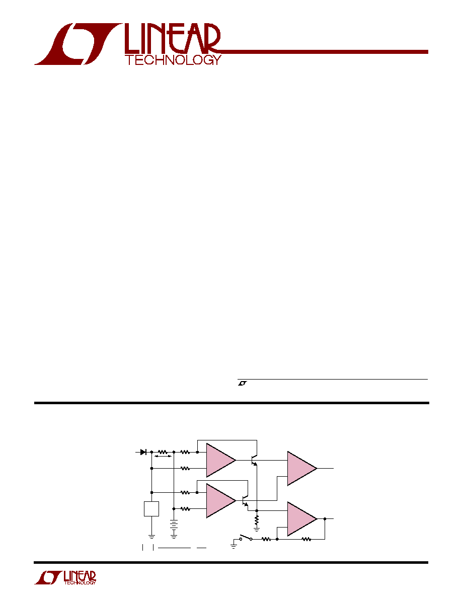
+
+
RA
2k
Q2
2N3904
S1
S1 = OPEN, GAIN = 1
S1 = CLOSED, GAIN = 10
R
A
= R
B
V
S
= 5V, 0V
10k
90.9k
V
OUT
LOGIC
14901A TA01
LOGIC HIGH (5V) = CHARGING
LOGIC LOW (0V) = DISCHARGING
R
G
10k
Q1
2N3904
R
S
0.2
CHARGER
VOLTAGE
1/2 LT1490A
1/2 LT1490A
R
A
´
2k
R
B
2k
V
BATT
= 12V
I
BATT
+
R
B
´
2k
LOAD
+
+
V
OUT
(R
S
)(R
G
/R
A
)(GAIN)
V
OUT
GAIN
I
BATT
= = AMPS
1/2 LT1490A
1/2 LT1490A
, LTC and LT are registered trademarks of Linear Technology Corporation.
Over-The-Top is a trademark of Linear Technology Corporation.
DESCRIPTIO
U
FEATURES
APPLICATIO S
U
TYPICAL APPLICATIO
U
2
LT1490A
ABSOLUTE
M
AXI
M
U
M
RATINGS
W
W
W
U
Total Supply Voltage (V
+
to V
) ............................. 44V
Differential Input Voltage ........................................ 44V
Input Current .....................................................
±
12mA
Output Short-Circuit Duration (Note 2) ........ Continuous
Junction Temperature .......................................... 150
°
C
PACKAGE/ORDER I
N
FOR
M
ATIO
N
W
U
U
Consult factory for Military grade parts.
LT1490ACN8
LT1490ACS8
LT1490AIN8
LT1490AIS8
SYMBOL
PARAMETER
CONDITIONS
MIN
TYP
MAX
UNITS
V
OS
Input Offset Voltage (Note 5)
N8, S8 Package
110
500
µ
V
0
°
C
T
A
70
°
C
q
700
µ
V
40
°
C
T
A
85
°
C
q
800
µ
V
MS8 Package
220
1000
µ
V
0
°
C
T
A
70
°
C
q
1200
µ
V
40
°
C
T
A
85
°
C
q
1400
µ
V
Input Offset Voltage Drift (Note 9)
40
°
C
T
A
85
°
C
q
2
4
µ
V/
°
C
I
OS
Input Offset Current
q
0.2
0.8
nA
V
CM
= 44V (Note 6)
q
0.8
µ
A
I
B
Input Bias Current
q
1
8
nA
V
CM
= 44V (Note 6)
q
3
10
µ
A
V
S
= 0V
0.3
nA
Input Noise Voltage
0.1Hz to 10Hz
1
µ
V
P-P
e
n
Input Noise Voltage Density
f = 1kHz
50
nV/
Hz
i
n
Input Noise Current Density
f = 1kHz
0.03
pA/
Hz
R
IN
Input Resistance
Differential
6
17
M
Common Mode, V
CM
= 0V to 44V
4
11
M
ELECTRICAL CHARACTERISTICS
T
JMAX
= 150
°
C,
JA
= 250
°
C/ W
S8 PART MARKING
MS8 PART MARKING
ORDER PART
NUMBER
LTNG
LTPU
1490A
1490AI
LT1490ACMS8
LT1490AIMS8
Operating Temperature Range
(Note 3) ............................................. 40
°
C to 85
°
C
Specified Temperature Range (Note 4) .. 40
°
C to 85
°
C
Storage Temperature Range ................ 65
°
C to 150
°
C
Lead Temperature (Soldering, 10 sec)................. 300
°
C
T
JMAX
= 150
°
C,
JA
= 130
°
C/ W (N8)
T
JMAX
= 150
°
C,
JA
= 190
°
C/ W (S8)
1
2
3
4
8
7
6
5
TOP VIEW
N8 PACKAGE
8-LEAD PDIP
S8 PACKAGE
8-LEAD PLASTIC SO
V
+
OUT B
IN B
+IN B
A
B
OUT A
IN A
+IN A
V
ORDER PART
NUMBER
1
2
3
4
OUT A
IN A
+IN A
V
8
7
6
5
V
+
OUT B
IN B
+IN B
TOP VIEW
MS8 PACKAGE
8-LEAD PLASTIC MSOP
(Note 1)
The
q
denotes specifications which apply over the full operating temperature
range, otherwise specifications are at T
A
= 25
°
C. V
S
= 3V, 0V; V
S
= 5V, 0V unless otherwise noted. (Note 4)
3
LT1490A
SYMBOL
PARAMETER
CONDITIONS
MIN
TYP
MAX
UNITS
V
OS
Input Offset Voltage (Note 5)
N8, S8 Package
150
700
µ
V
0
°
C
T
A
70
°
C
q
950
µ
V
40
°
C
T
A
85
°
C
q
1100
µ
V
MS8 Package
250
1200
µ
V
0
°
C
T
A
70
°
C
q
1350
µ
V
40
°
C
T
A
85
°
C
q
1500
µ
V
SYMBOL
PARAMETER
CONDITIONS
MIN
TYP
MAX
UNITS
C
IN
Input Capacitance
4.6
pF
Input Voltage Range
q
0
44
V
CMRR
Common Mode Rejection Ratio
V
CM
= 0V to V
CC
1V
q
84
98
dB
(Note 6)
V
CM
= 0V to 44V
q
80
98
dB
A
VOL
Large-Signal Voltage Gain
V
S
= 3V, V
O
= 500mV to 2.5V, R
L
= 10k
200
1500
V/mV
0
°
C
T
A
70
°
C
q
133
V/mV
40
°
C
T
A
85
°
C
q
100
V/mV
V
S
= 5V, V
O
= 500mV to 4.5V, R
L
= 10k
400
1500
V/mV
0
°
C
T
A
70
°
C
q
250
V/mV
40
°
C
T
A
85
°
C
q
200
V/mV
V
OL
Output Voltage Swing Low
V
S
= 3V, No Load
q
3
10
mV
V
S
= 3V, I
SINK
= 5mA
q
250
450
mV
V
S
= 5V, No Load
q
3
10
mV
V
S
= 5V, I
SINK
= 5mA
q
250
500
mV
V
S
= 5V, I
SINK
= 10mA
330
500
mV
V
OH
Output Voltage Swing High
V
S
= 3V, No Load
q
2.95
2.978
V
V
S
= 3V, I
SOURCE
= 5mA
q
2.55
2.6
V
V
S
= 5V, No Load
q
4.95
4.978
V
V
S
= 5V, I
SOURCE
= 10mA
q
4.30
4.6
V
I
SC
Short-Circuit Current (Note 2)
V
S
= 3V, Short to GND
10
15
mA
V
S
= 3V, Short to V
CC
10
30
mA
V
S
= 5V, Short to GND
15
25
mA
V
S
= 5V, Short to V
CC
15
30
mA
PSRR
Power Supply Rejection Ratio
V
S
= 2.5V to 12.5V, V
CM
= V
O
= 1V
q
84
98
dB
Minimum Operating Supply Voltage
q
2
2.5
V
Reverse Supply Voltage
I
S
= 100
µ
A per Amplifier
q
18
27
V
I
S
Supply Current per Amplifier
40
50
µ
A
(Note 7)
q
55
µ
A
GBW
Gain Bandwidth Product
f = 1kHz
110
180
kHz
(Note 6)
0
°
C
T
A
70
°
C
q
100
kHz
40
°
C
T
A
85
°
C
q
90
kHz
SR
Slew Rate
A
V
= 1, R
L
=
0.035
0.06
V/
µ
s
(Note 8)
0
°
C
T
A
70
°
C
q
0.031
V/
µ
s
40
°
C
T
A
85
°
C
q
0.030
V/
µ
s
ELECTRICAL CHARACTERISTICS
The
q
denotes specifications which apply over the full operating temperature
range, otherwise specifications are at T
A
= 25
°
C. V
S
= 3V, 0V; V
S
= 5V, 0V unless otherwise noted. (Note 4)
The
q
denotes specifications which apply over the full operating temperature range, otherwise specifications are at T
A
= 25
°
C.
V
S
=
±
15V unless otherwise noted. (Note 4)
4
LT1490A
SYMBOL
PARAMETER
CONDITIONS
MIN
TYP
MAX
UNITS
Input Offset Voltage Drift (Note 9)
40
°
C
T
A
85
°
C
q
2
6
µ
V/
°
C
I
OS
Input Offset Current
q
0.2
0.8
nA
I
B
Input Bias Current
q
1
8
nA
Input Noise Voltage
0.1Hz to 10Hz
1
µ
V
P-P
e
n
Input Noise Voltage Density
f = 1kHz
50
nV/
Hz
i
n
Input Noise Current Density
f = 1kHz
0.03
pA/
Hz
R
IN
Input Resistance
Differential
6
17
M
Common Mode, V
CM
= 15V to 14V
15000
M
C
IN
Input Capacitance
4.6
pF
Input Voltage Range
q
15
29
V
CMRR
Common Mode Rejection Ratio
V
CM
= 15V to 29V
q
80
98
dB
A
VOL
Large-Signal Voltage Gain
V
O
=
±
14V, R
L
= 10k
100
250
V/mV
0
°
C
T
A
70
°
C
q
75
V/mV
40
°
C
T
A
85
°
C
q
50
V/mV
V
O
Output Voltage Swing
No Load
q
±
14.9
±
14.978
V
I
OUT
=
±
5mA
q
±
14.5
±
14.750
V
I
OUT
=
±
10mA
±
14.5
±
14.670
V
I
SC
Short-Circuit Current (Note 2)
Short to GND
±
20
±
25
mA
0
°
C
T
A
70
°
C
q
±
15
mA
40
°
C
T
A
85
°
C
q
±
10
mA
PSRR
Power Supply Rejection Ratio
V
S
=
±
1.25V to
±
22V
q
88
98
dB
I
S
Supply Current per Amplifier
50
70
µ
A
q
85
µ
A
GBW
Gain Bandwidth Product
f = 1kHz
125
200
kHz
0
°
C
T
A
70
°
C
q
110
kHz
40
°
C
T
A
85
°
C
q
100
kHz
SR
Slew Rate
A
V
= 1, R
L
=
,
V
O
=
±
10V,
0.0375
0.07
V/
µ
s
Measure at V
O
=
±
5V
0
°
C
T
A
70
°
C
q
0.0330
V/
µ
s
40
°
C
T
A
85
°
C
q
0.0300
V/
µ
s
ELECTRICAL CHARACTERISTICS
Note 1: Absolute Maximum Ratings are those values beyond which the life
of the device may be impaired.
Note 2: A heat sink may be required to keep the junction temperature
below absolute maximum. This depends on the power supply voltage and
how many amplifiers are shorted.
Note 3: The LT1490AC and LT1490AI are guaranteed functional over the
operating temperature range of 40
°
C to 85
°
C.
Note 4: The LT1490AC is guaranteed to meet specified performance from
0
°
C to 70
°
C. The LT1490AC is designed, characterized and expected to
meet specified performance from 40
°
C to 85
°
C but is not tested or QA
sampled at these temperatures. The LT1490I is guaranteed to meet
specified performance from 40
°
C to 85
°
C.
Note 5: ESD (Electrostatic Discharge) sensitive device. Extensive use of
ESD protection devices are used internal to the LT1490A. However, high
electrostatic discharge can damage or degrade the device. Use proper
ESD handling precautions.
Note 6: V
S
= 5V limits are guaranteed by correlation to V
S
= 3V and
V
S
=
±
15V tests.
Note 7: V
S
= 3V limits are guaranteed by correlation to V
S
= 5V and
V
S
=
±
15V tests.
Note 8: Guaranteed by correlation to slew rate at V
S
=
±
15V and GBW
at V
S
= 3V and V
S
=
±
15V tests.
Note 9: This parameter is not 100% tested.
The
q
denotes specifications which apply over the full operating temperature
range, otherwise specifications are at T
A
= 25
°
C. V
S
=
±
15V unless otherwise noted. (Note 4)
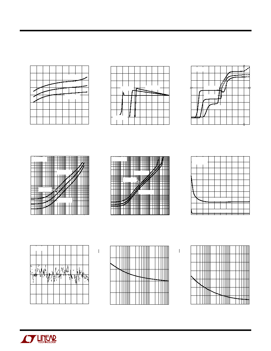
5
LT1490A
TOTAL SUPPLY VOLTAGE (V)
0
0
SUPPLY CURRENT PER AMPLIFIER (
µ
A)
10
30
40
50
70
10
20
25
45
1490A G01
20
80
60
5
15
30
35
40
T
A
= 125
°
C
T
A
= 25
°
C
T
A
= 55
°
C
Supply Current vs Supply Voltage
TOTAL SUPPLY VOLTAGE (V)
0
CHANGE IN INPUT OFFSET VOLTAGE (
µ
V)
200
400
4
1490A G02
0
200
100
300
100
300
400
1
2
3
5
T
A
=
25
°
C
T
A
=
125
°
C
T
A
=
55
°
C
Minimum Supply Voltage
Input Bias Current
vs Common Mode Voltage
Output Saturation Voltage
vs Input Overdrive
Output Saturation Voltage
vs Load Current (Output High)
Output Saturation Voltage
vs Load Current (Output Low)
0.1Hz to 10Hz Noise Voltage
FREQUENCY (Hz)
1
40
INPUT NOISE VOLTAGE DENSITY (nV/
Hz)
50
60
70
10
100
1k
1490A G08
30
80
FREQUENCY (Hz)
1
INPUT NOISE CURRENT DENSITY (pA/
Hz)
10
100
1k
1490A G09
0.20
0.25
0.30
0.35
0.15
0.10
0.05
0
TIME (SEC)
NOISE VOLTAGE (400nV/DIV)
2
4
6
8
1490A G07
10
1
0
3
5
7
9
V
S
=
±
2.5V
Noise Voltage Density
vs Frequency
Input Noise Current vs Frequency
TYPICAL PERFOR A CE CHARACTERISTICS
U
W
COMMON MODE VOLTAGE (V)
4.0
INPUT BIAS CURRENT (nA)
5000
3000
1000
30
20
10
0
10
5.6
1490A G03
4.4
4.8
5.2
44
T
A
= 55
°
C
T
A
= 25
°
C
T
A
= 125
°
C
V
S
= 5V, 0V
SOURCING LOAD CURRENT (A)
1
µ
OUTPUT SATURATION VOLTAGE (V)
100m
10m
1490A G04
10m
10
µ
100
µ
1m
100m
1
T
A
= 125
°
C
V
S
= 5V, 0V
T
A
= 25
°
C
T
A
= 55
°
C
SINKING LOAD CURRENT (A)
0.1
µ
1m
OUTPUT SATURATION VOLTAGE (V)
10m
100m
1
1
µ
10
µ
100
µ
1m
1490A G05
10m
100m
T
A
= 125
°
C
V
S
= 5V, 0V
T
A
= 25
°
C
T
A
= 55
°
C
INPUT OVERDRIVE (mV)
0
OUTPUT SATURATION VOLTAGE (mV)
60
80
100
40
1490A G06
40
20
50
70
90
30
10
0
10
20
30
50
OUTPUT HIGH
OUTPUT LOW
V
S
= 5V, 0V
NO LOAD