 | –≠–ª–µ–∫—Ç—Ä–æ–Ω–Ω—ã–π –∫–æ–º–ø–æ–Ω–µ–Ω—Ç: LT1497 | –°–∫–∞—á–∞—Ç—å:  PDF PDF  ZIP ZIP |
1
LT1497
Dual 125mA, 50MHz
Current Feedback Amplifier
≠
+
≠
+
560
560
560
V
IN
68.1
68.1
1:1*
135
560
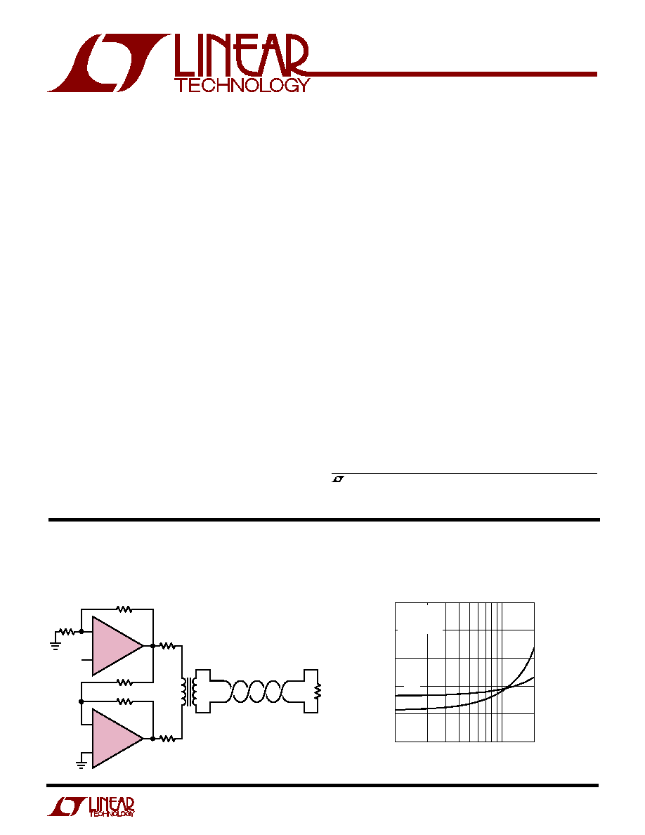
1/2 LT1497
1/2 LT1497
*MIDCOM 671-7807
1419 TA01
2nd and 3rd Harmonic Distortion of
HDSL2 Single Pair Line Driver
FREQUENCY (Hz)
100k
≠ 90
DISTORTION (dBc)
≠ 80
≠ 70
≠ 60
≠ 50
1M
2M
1497 TA02
≠ 40
V
S
=
±
5V
V
IN
=
±
1.25V
V
OUT
=
±
2.5V
3RD
2ND
HDSL2 Single Pair Line Driver
s
Minimum Output Current:
±
125mA
s
Maximum Supply Current per Amp: 7mA, V
S
=
±
5V
s
Bandwidth: 50MHz, V
S
=
±
15V
s
Slew Rate: 900V/
µ
s, V
S
=
±
15V
s
Wide Supply Range: V
S
=
±
2.5V to
±
15V
(Enhanced
JA
16-Pin SO Package)
s
Enhanced
JA
SO-8 Package for
±
5V Operation
s
0.02% Differential Gain: A
V
= 2, R
L
= 150
s
0.015
∞
Differential Phase: A
V
= 2, R
L
= 150
s
±
13V Output Swing: I
L
= 100mA, V
S
=
±
15V
s
±
3.1V Output Swing: I
L
= 100mA, V
S
=
±
5V
s
55ns Settling Time to 0.1%, 10V Step
s
Thermal Shutdown Protection
FEATURES
DESCRIPTIO
N
U
The LT
Æ
1497 dual current feedback amplifier features low
power, high output drive, excellent video characteristics
and outstanding distortion performance. From a low 7mA
maximum supply current per amplifier, the LT1497 drives
±
100mA with only 1.9V of headroom. Twisted pairs can be
driven differentially with ≠ 70dBc distortion up to 1MHz for
±
40mA peak signals.
The LT1497 is available in a low thermal resistance 16-pin
SO package for operation with supplies up to
±
15V. For
±
5V operation the device is also available in a low thermal
resistance SO-8 package. The device has thermal and
current limit circuits that protect against fault conditions.
The LT1497 is manufactured on Linear Technology's
complementary bipolar process. The device has charac-
teristics that bridge the performance between the LT1229
and LT1207 dual current feedback amplifiers. The LT1229
has 30mA output drive, 100MHz bandwidth and 12mA
supply current. The LT1207 has 250mA output drive,
60MHz bandwidth and 40mA supply current.
, LTC and LT are registered trademarks of Linear Technology Corporation.
APPLICATIO
N
S
U
s
Twisted-Pair Drivers
s
Video Amplifiers
s
Cable Drivers
s
Test Equipment Amplifiers
s
Buffers
TYPICAL APPLICATIO
N
U

2
LT1497
ABSOLUTE
M
AXI
M
U
M
RATINGS
W
W
W
U
Total Supply Voltage (V
+
to V
≠
)
LT1497CS8.......................................................... 14V
LT1497CS............................................................ 36V
Noninverting Input Current ...................................
±
2mA
Output Short-Circuit Duration (Note 1) .......... Continuous
Operating Temperature Range (Note 2) ... ≠ 40
∞
C to 85
∞
C
Specified Temperature Range ...................... 0
∞
C to 70
∞
C
Maximum Junction Temperature (See Below) ....... 150
∞
C
Storage Temperature Range .................. ≠ 65
∞
C to 150
∞
C
Lead Temperature (Soldering, 10 sec)................... 300
∞
C
PACKAGE/ORDER I
N
FOR
M
ATIO
N
W
U
U
T
JMAX
= 150
∞
C,
JA
= 40
∞
C/ W (NOTE 3)
ORDER PART
NUMBER
ORDER PART
NUMBER
S8 PART MARKING
1497
LT1497CS8
T
JMAX
= 150
∞
C,
JA
= 80
∞
C/ W (NOTE 3)
1
2
3
4
8
7
6
5
TOP VIEW
S8 PACKAGE
8-LEAD PLASTIC SO
OUT A
≠IN A
+IN A
V
≠
V
+
OUT B
≠IN B
+IN B
A
B
LT1497CS
Consult factory for Industrial and Military grade parts.
TOP VIEW
S PACKAGE
16-LEAD PLASTIC SO
1
2
3
4
5
6
7
8
16
15
14
13
12
11
10
9
V
≠
NC
OUT A
≠IN A
+IN A
V
≠
NC
V
≠
V
≠
NC
V
+
OUT B
≠IN B
+IN B
NC
V
≠
A
B
ELECTRICAL CHARACTERISTICS
V
CM
= 0V,
±
2.5V
V
S
±
15V (LT1497CS),
±
2.5V
V
S
±
5V (LT1497CS8), pulse tested unless otherwise noted.
SYMBOL
PARAMETER
CONDITIONS
MIN
TYP
MAX
UNITS
V
OS
Input Offset Voltage
T
A
= 25
∞
C
±
3
±
10
mV
q
±
15
mV
Input Offset Voltage Matching
T
A
= 25
∞
C
±
1
±
3.5
mV
q
±
5.0
mV
Input Offset Voltage Drift
q
10
µ
V/
∞
C
I
IN
+
Noninverting Input Current
T
A
= 25
∞
C
±
1
±
3
µ
A
q
±
10
µ
A
Noninverting Input Current Matching
T
A
= 25
∞
C
±
0.3
±
1.0
µ
A
q
±
1.5
µ
A
I
IN
≠
Inverting Input Current
T
A
= 25
∞
C
±
7
±
20
µ
A
q
±
40
µ
A
Inverting Input Current Matching
T
A
= 25
∞
C
±
3
±
10
µ
A
q
±
15
µ
A
e
n
Input Noise Voltage Density
f = 1kHz, R
F
= 1k, R
G
= 10
, R
S
= 0
3
nV/
Hz
+ i
n
Noninverting Input Noise Current Density
f = 1kHz, R
F
= 1k, R
G
= 10
, R
S
= 10k
2
pA/
Hz
≠ i
n
Inverting Input Noise Current Density
f = 1kHz, R
F
= 1k, R
G
= 10
, R
S
= 10k
20
pA/
Hz
R
IN
Input Resistance
V
IN
=
±
13V, V
S
=
±
15V
q
1.5
10
M
V
IN
=
±
3V, V
S
=
±
5V
q
1.5
8
M
V
IN
=
±
0.5V, V
S
=
±
2.5V
q
1.5
8
M
C
IN
Input Capacitance
3
pF

3
LT1497
ELECTRICAL CHARACTERISTICS
V
CM
= 0V,
±
2.5V
V
S
±
15V (LT1497CS),
±
2.5V
V
S
±
5V (LT1497CS8), pulse tested unless otherwise noted.
SYMBOL
PARAMETER
CONDITIONS
MIN
TYP
MAX
UNITS
Input Voltage Range
V
S
=
±
15V
q
±
13
±
14
V
V
S
=
±
5V
q
±
3.0
±
4.0
V
V
S
=
±
2.5V
q
±
0.5
±
1.5
V
CMRR
Common Mode Rejection Ratio
V
S
=
±
15V, V
CM
=
±
13V, T
A
= 25
∞
C
55
62
dB
q
53
dB
V
S
=
±
5V, V
CM
=
±
3V, T
A
= 25
∞
C
54
60
dB
q
52
dB
V
S
=
±
2.5V, V
CM
=
±
0.5V, T
A
= 25
∞
C
52
56
dB
q
50
dB
Inverting Input Current
V
S
=
±
15V, V
CM
=
±
13V
q
2.0
10
µ
A/V
Common Mode Rejection
V
S
=
±
5V, V
CM
=
±
3V
q
2.5
10
µ
A/V
V
S
=
±
2.5V, V
CM
=
±
0.5V
q
3.0
10
µ
A/V
PSRR
Power Supply Rejection Ratio
V
S
=
±
2V to
±
15V, T
A
= 25
∞
C
66
76
dB
q
63
dB
V
S
=
±
2V to
±
5V, T
A
= 25
∞
C
66
76
dB
q
63
dB
Noninverting Input Current
V
S
=
±
2V to
±
15V
q
5
50
nA/V
Power Supply Rejection
V
S
=
±
2V to
±
5V
q
5
50
nA/V
Inverting Input Current
V
S
=
±
2V to
±
15V
q
0.1
2
µ
A/V
Power Supply Rejection
V
S
=
±
2V to
±
5V
q
0.1
2
µ
A/V
A
VOL
Large-Signal Voltage Gain
V
S
=
±
15V, V
OUT
=
±
10V, R
L
= 150
q
66
80
dB
V
S
=
±
5V, V
OUT
=
±
2.5V, R
L
= 50
q
66
80
dB
V
S
=
±
2.5V, V
OUT
=
±
0.5V, R
L
= 50
q
66
80
dB
R
OL
Transresistance,
V
OUT
/
I
IN
≠
V
S
=
±
15V, V
OUT
=
±
10V, R
L
= 150
q
100
500
k
V
S
=
±
5V, V
OUT
=
±
2.5V, R
L
= 50
q
100
500
k
V
S
=
±
2.5V, V
OUT
=
±
0.5V, R
L
= 50
q
100
300
k
V
OUT
Maximum Output Swing
V
S
=
±
15V, R
L
= 150
, T
A
= 25
∞
C
±
12.80
±
13.15
V
q
±
12.60
V
V
S
=
±
15V, I
L
=
±
100mA, T
A
= 25
∞
C
±
12.65
±
13.0
V
q
±
12.55
V
V
S
=
±
5V, R
L
= 50
, T
A
= 25
∞
C
±
3.20
±
3.45
V
q
±
3.10
V
V
S
=
±
5V, I
L
=
±
100mA, T
A
= 25
∞
C
±
2.75
±
3.10
V
q
±
2.65
V
V
S
=
±
2.5V, R
L
= 50
, T
A
= 25
∞
C
±
1.25
±
1.45
V
q
±
1.15
V
V
S
=
±
2.5V, I
L
=
±
50mA, T
A
= 25
∞
C
±
1.00
±
1.15
V
q
±
0.90
V
I
OUT
Maximum Output Current
R
L
= 1
, V
S
=
±
15V
q
±
125
±
220
mA
R
L
= 1
, V
S
=
±
5V
q
±
125
±
220
mA
R
L
= 1
, V
S
=
±
2.5V
±
140
mA
I
S
Supply Current per Amplifier
V
S
=
±
2.5V to
±
5V, T
A
= 25
∞
C
6.0
7.0
mA
q
8.0
mA
V
S
=
±
15V, T
A
= 25
∞
C
7.0
9.0
mA
q
10.5
mA
Channel Separation
V
S
=
±
15V, V
OUT
=
±
10V, R
L
= 150
q
100
120
dB
V
S
=
±
5V, V
OUT
=
±
2.5V, R
L
= 50
q
100
115
dB
4
LT1497
ELECTRICAL CHARACTERISTICS
SYMBOL
PARAMETER
CONDITIONS
MIN
TYP
MAX
UNITS
SR
Slew Rate
V
S
=
±
15V, T
A
= 25
∞
C (Note 4)
500
900
V/
µ
s
q
400
V/
µ
s
V
S
=
±
5V, T
A
= 25
∞
C (Note 4)
200
350
V/
µ
s
q
150
V/
µ
s
BW
Small-Signal Bandwidth
V
S
=
±
15V, R
F
= R
G
= 560
, R
L
= 100
50
MHz
V
S
=
±
5V, R
F
= R
G
= 560
, R
L
= 100
35
MHz
V
S
=
±
2.5V, R
F
= R
G
= 560
, R
L
= 100
30
MHz
t
r
Small-Signal Rise Time
V
S
=
±
15V, R
F
= R
G
= 560
, R
L
= 100
7.5
ns
V
S
=
±
5V, R
F
= R
G
= 560
, R
L
= 100
9.5
ns
V
S
=
±
2.5V, R
F
= R
G
= 560
, R
L
= 100
11
ns
Overshoot
V
S
=
±
15V, R
F
= R
G
= 560
, R
L
= 100
15
%
V
S
=
±
5V, R
F
= R
G
= 560
, R
L
= 100
12
%
V
S
=
±
2.5V, R
F
= R
G
= 560
, R
L
= 100
10
%
Propagation Delay
V
S
=
±
15V, R
F
= R
G
= 560
, R
L
= 100
6.8
ns
V
S
=
±
5V, R
F
= R
G
= 560
, R
L
= 100
8.4
ns
V
S
=
±
2.5V, R
F
= R
G
= 560
, R
L
= 100
9.7
ns
t
s
Settling Time
V
S
=
±
15V, 10V Step, 0.1%, A
V
= ≠ 1
55
ns
V
S
=
±
5V, 5V Step, 0.1%, A
V
= ≠ 1
50
ns
Differential Gain (Note 5)
V
S
=
±
15V, R
F
= R
G
= 510
, R
L
= 150
0.02
%
V
S
=
±
15V, R
F
= R
G
= 510
, R
L
= 50
0.19
%
V
S
=
±
5V, R
F
= R
G
= 510
, R
L
= 150
0.08
%
V
S
=
±
5V, R
F
= R
G
= 510
, R
L
= 50
0.41
%
Differential Phase (Note 5)
V
S
=
±
15V, R
F
= R
G
= 510
, R
L
= 150
0.015
Deg
V
S
=
±
15V, R
F
= R
G
= 510
, R
L
= 50
0.235
Deg
V
S
=
±
5V, R
F
= R
G
= 510
, R
L
= 150
0.045
Deg
V
S
=
±
5V, R
F
= R
G
= 510
, R
L
= 50
0.310
Deg
V
CM
= 0V,
±
2.5V
V
S
±
15V (LT1497CS),
±
2.5V
V
S
±
5V (LT1497CS8), pulse tested unless otherwise noted.
The
q
denotes specifications which apply over the full operating
temperature range.
Note 1: Applies to short circuits to ground only. A short circuit between the
output and either supply may damage the part when operated on supplies
greater than
±
10V
Note 2: The LT1497 is designed, characterized and expected to operate
over the temperature range of ≠ 40
∞
C to 85
∞
C, but is not tested at ≠ 40
∞
C
and 85
∞
C. Guaranteed industrial grade parts are available, consult factory.
Note 3: Thermal resistance varies depending upon the amount of PC board
metal attached to the device.
JA
is specified for a 2500mm
2
test board
covered with 2oz copper on both sides.
Note 4: Slew rate is measured between
±
5V on a
±
10V output signal while
operating on
±
15V supplies with R
F
= 453
, R
G
= 49.9
and R
L
= 150
.
On
±
5V supplies slew rate is measured between
±
1V on a
±
3V output
signal. The slew rate is much higher when the input is overdriven and
when the amplifier is operated inverting. See the Applications Information
section.
Note 5: NTSC composite video with an amplifier output level of 2V peak.

5
LT1497
V
S
=
±
5V, Peaking
1dB
A
V
R
L
R
F
R
G
≠ 3dB BW (MHz)
≠ 1
150
510
510
45.0
50
560
560
32.0
20
560
560
23.2
1
150
510
≠
44.3
50
560
≠
31.7
20
560
≠
22.9
2
150
510
510
41.7
50
560
560
30.4
20
560
560
21.9
10
150
270
30
28.1
50
270
30
21.9
20
270
30
14.6
S
M
ALL-SIG
N
AL BA
N
DWIDTH
U
U
W
V
S
=
±
15V, Peaking
1dB
A
V
R
L
R
F
R
G
≠ 3dB BW (MHz)
≠ 1
150
560
560
59.2
50
560
560
43.1
20
620
620
30.0
1
150
560
≠
57.0
50
560
≠
42.7
20
560
≠
30.3
2
150
510
510
59.1
50
560
560
41.7
20
620
620
20.7
10
150
270
30
43.4
50
270
30
30.9
20
270
30
19.0
Voltage Gain and Phase
vs Frequency, Gain = 20dB
FREQUENCY (MHz)
0.1
16
VOLTAGE GAIN (dB)
PHASE SHIFT (DEG)
18
20
22
24
1
10
100
1497 G04
14
12
10
8
26
28
270
225
180
135
90
45
0
±
15V
GAIN
PHASE
±
5V
±
5V
±
15V
R
L
= 100
R
F
= 270
R
G
= 30
SUPPLY VOLTAGE (
±
V)
0
0
≠
3dB BANDWIDTH (MHz)
10
30
40
50
12
90
1497 G05
20
6
18
10
4
16
8
2
14
60
70
80
PEAKING
1dB
PEAKING
5dB
R
F
= 430
R
F
= 270
R
F
= 750
R
F
= 560
R
F
= 1k
GAIN = 10
R
L
= 1k
SUPPLY VOLTAGE (
±
V)
0
0
≠
3dB BANDWIDTH (MHz)
10
30
40
50
12
90
1497 G06
20
6
18
10
4
16
8
2
14
60
70
80
PEAKING
1dB
PEAKING
5dB
R
F
= 270
R
F
= 1k
GAIN = 10
R
L
= 100
R
F
= 430
R
F
= 560
R
F
= 750
≠ 3dB Bandwidth
vs Supply Voltage
≠ 3dB Bandwidth
vs Supply Voltage
SUPPLY VOLTAGE (
±
V)
0
0
≠
3dB BANDWIDTH (MHz)
10
30
40
50
12
90
1497 G03
20
6
18
10
4
16
8
2
14
60
70
80
PEAKING
1dB
PEAKING
5dB
R
F
= 470
R
F
= 560
R
F
= 750
R
F
= 1k
GAIN = 2
R
L
= 100
FREQUENCY (MHz)
0.1
3
VOLTAGE GAIN (dB)
PHASE SHIFT (DEG)
4
5
6
7
1
10
100
1497 G01
2
1
0
≠1
8
9
270
225
180
135
90
45
0
±
15V
GAIN
PHASE
±
5V
±
5V
±
15V
R
L
= 100
R
F
= R
G
= 560
Voltage Gain and Phase
vs Frequency, Gain = 6dB
SUPPLY VOLTAGE (
±
V)
0
0
≠
3dB BANDWIDTH (MHz)
10
30
40
50
12
90
1497 G02
20
6
18
10
4
16
8
2
14
60
70
80
PEAKING
1dB
PEAKING
5dB
R
F
= 470
R
F
= 560
R
F
= 750
R
F
= 1k
GAIN = 2
R
L
= 1k
≠ 3dB Bandwidth
vs Supply Voltage
≠ 3dB Bandwidth
vs Supply Voltage
TYPICAL PERFOR
M
A
N
CE CHARACTERISTICS
U
W