 | –≠–ª–µ–∫—Ç—Ä–æ–Ω–Ω—ã–π –∫–æ–º–ø–æ–Ω–µ–Ω—Ç: LT1573 | –°–∫–∞—á–∞—Ç—å:  PDF PDF  ZIP ZIP |

1
LT1573
Low Dropout
PNP Regulator Driver
Figure 1. 3.3V, 5A Microprocessor Supply
s
Low Cost Solution for High Current, Low Dropout
Regulators
s
Fast Transient Response Needs Much Less
Bulk Capacitance
s
Latching Overload Protection Minimizes
Heat Sink Size
s
Precision Output Voltage (1%)
s
Single Supply Operation: V
IN
= 2.8V to 10V
s
Small Surface Mount Package
s
Capable of Very Low Dropout Voltage (<0.2V)
s
Fixed or Adjustable Outputs
s
Shutdown
s
3.3V to 2.5V Regulators
s
Microprocessor Power Sources
s
Post Regulator for Switching Supplies
s
High Efficiency Linear Regulators
s
Ultralow Dropout Regulators
s
Low Voltage Linear Regulators
The LT
Æ
1573 is a regulator driver IC designed to provide
a low cost solution for applications requiring high current,
low dropout and fast transient response. When combined
with an external PNP power transistor, this device pro-
vides load current up to 5A with dropout voltages as low
as 0.35V. The LT1573 circuitry is designed for extremely
fast transient response. This greatly reduces bulk storage
capacitance when the regulator is used in applications
with fast, high current load transients.
To keep cost and complexity low, the LT1573 uses a new
time-delayed latching overcurrent protection technique
that requires no external current sense resistor. Base drive
is limited for instantaneous protection, and a time-delayed
latch protects the regulator from continuous short
circuits.
The LT1573 is available as an adjustable regulator with an
output range of 1.27V to 6.8V and with fixed output
voltages of 2.5V, 2.8V and 3.3V. Output accuracy is better
than 1% to meet the critical regulation requirement of fast
microprocessors. A special 8-pin, fused-lead surface mount
package is used to minimize regulator footprint and pro-
vide adequate heat sinking.
, LTC and LT are registered trademarks of Linear Technology Corporation.
COMP
V
OUT
V
IN
DRIVE
FB
LATCH
SHDN
GND
LT1573
+
C
TIME
C
OUT2
220
µ
F
TANT
C
OUT1
1
µ
F
CER
◊
24
C
C
100pF
V
IN
5V
R
C
1k
R
D
24
V
OUT
3.3V
GND
1573 F01
R
B
50
R1
1.6k
R2
1k
LOAD
+
+
Q
OUT
MOTOROLA
D45H11
V
OUT
= 1.265V (1 + R1/R2)
FOR T < 45
∞
C, C
OUT1
= 24
◊
1
µ
F Y5V CERAMIC SURFACE MOUNT CAPACITORS.
FOR T > 45
∞
C, C
OUT1
= 24
◊
1
µ
F X7R CERAMIC SURFACE MOUNT CAPACITORS.
PLACE C
OUT1
IN THE MICROPROCESSOR SOCKET CAVITY
C
IN
100
µ
F
TANT
Transient Response for
0.2A to 5A Output Load Step
10
µ
s/DIV
1573 F01a
50mV/DIV
2.5A/DIV
FEATURES
DESCRIPTIO
U
APPLICATIO S
U
TYPICAL APPLICATIO
U

2
LT1573
ORDER PART
NUMBER
S8 PART MARKING
157333
1573I
1573
157325
157328
Consult factory for Military grade parts.
The
q
denotes specifications that apply over the full operating temperature
range, otherwise specifications are at T
A
= 25
∞
C. V
IN
= 5V, V
DRIVE
= 3V, unless otherwise noted.
(Note 1)
Input Pin Voltage (V
IN
to GND) ............................... 10V
Drive Pin Voltage (V
DRIVE
to GND) .......................... 10V
Output Pin Voltage (V
OUT
to GND) .......................... 10V
Shutdown Pin Voltage (V
SHDN
to GND) .................. 10V
Operating Junction Temperature Range
LT1573C ............................................... 0
∞
C to 125
∞
C
LT1573I ............................................ ≠40
∞
C to 125
∞
C
Storage Temperature Range ................ ≠ 65
∞
C to 150
∞
C
Lead Temperature (Soldering, 10 sec.)................ 300
∞
C
TOP VIEW
COMP
V
OUT
V
IN
DRIVE
FB
LATCH
SHDN
GND
S8 PACKAGE
8-LEAD PLASTIC SO
1
2
3
4
8
7
6
5
T
JMAX
= 125
∞
C,
JA
= 85
∞
C/ W
LT1573CS8
LT1573CS8-2.5
LT1573CS8-2.8
LT1573CS8-3.3
LT1573IS8
PARAMETER
CONDITIONS
MIN
TYP
MAX
UNITS
DC Characteristics
LT1573 Reference Voltage (Adjustable)(Note 2)
I
DRIVE
= 20mA, T
J
= 25
∞
C
1.252
1.265
1.278
V
5mA < I
DRIVE
< 250mA, 3V < V
IN
< 7V,
q
1.225
1.265
1.305
V
1.5V < V
DRIVE
< 7V
LT1573-3.3 Output Voltage (Note 2)
I
DRIVE
= 20mA. T
J
= 25
∞
C
3.267
3.3
3.333
V
5mA < I
DRIVE
< 250mA, 3.5V < V
IN
< 7V,
q
3.234
3.3
3.366
V
1.5V < V
DRIVE
< 7V
LT1573-2.8 Output Voltage (Note 2)
I
DRIVE
= 20mA, T
J
= 25
∞
C
2.772
2.8
2.828
V
5mA < I
DRIVE
< 250mA, 3V < V
IN
< 7V,
q
2.744
2.8
2.856
V
1.5V < V
DRIVE
< 7V
LT1573-2.5 Output Voltage (Note 2)
I
DRIVE
= 20mA, T
J
= 25
∞
C
2.475
2.5
2.525
V
5mA < I
DRIVE
< 250mA, 3V < V
IN
< 7V,
q
2.450
2.5
2.550
V
1.5V < V
DRIVE
< 7V
Line Regulation
LT1573 (V
FB
)
I
DRIVE
= 20mA, 3V < V
IN
< 7V
q
0.17
2
mV
LT1573-3.3 (V
OUT
)
I
DRIVE
= 20mA, 3.5V < V
IN
< 7V
q
0.34
5
mV
LT1573-2.8 (V
OUT
)
I
DRIVE
= 20mA, 3V < V
IN
< 7V
q
0.34
4
mV
LT1573-2.5 (V
OUT
)
I
DRIVE
= 20mA, 3V < V
IN
< 7V
q
0.25
4
mV
Load Regulation
LT1573 (V
FB
)
I
DRIVE
= 20mA to 250mA
q
7
30
mV
LT1573-3.3 (V
OUT
)
I
DRIVE
= 20mA to 250mA
q
18
40
mV
LT1573-2.8 (V
OUT
)
I
DRIVE
= 20mA to 250mA
q
15
34
mV
LT1573-2.5 (V
OUT
)
I
DRIVE
= 20mA to 250mA
q
13
30
mV
FB
Pin Bias Current (Adjustable Only)
V
FB
= 1.265V
q
0.8
5
µ
A
DRIVE Pin Current
V
FB
= 1.35V, V
DRIVE
= 7V
q
2
mA
V
FB
= 1.15V, V
DRIVE
= 1.5V
q
250
440
mA
DRIVE Pin Saturation Voltage
I
DRIVE
= 20mA, V
FB
= 1.15V
q
0.12
0.3
V
I
DRIVE
= 250mA, V
FB
= 1.15V
q
0.73
1.4
V
SHDN Pin Threshold Voltage
q
1.0
1.33
1.6
V
SHDN Pin Current
V
SHDN
= 5V
200
µ
A
ABSOLUTE AXI U RATI GS
W
W
W
U
PACKAGE/ORDER I FOR ATIO
U
U
W
ELECTRICAL CHARACTERISTICS

3
LT1573
PARAMETER
CONDITIONS
MIN
TYP
MAX
UNITS
LATCH Pin Latch-Off Threshold Voltage
q
0.8
1.4
2.2
V
LATCH Pin Charging Current
7
µ
A
LATCH Pin Latching Current
0.65
mA
V
IN
≠ V
OUT
Differential Threshold for Latch Disable
q
0.4
0.7
1.0
V
Input Quiescent Current
V
IN
= 7V
q
1.7
3.5
mA
Minimum Input Voltage for Bias Operation
q
2.8
V
Note 1: Absolute Maximum Ratings are those values beyond which the life
of the device may be impaired.
Note 2: Operating conditions are limited by maximum junction
temperature. The regulated feedback or output voltage specification will
not apply for all possible combinations of input voltage, drive voltage and
drive current. When operating at maximum drive current, the drive voltage
range must be limited. When operating at maximum input and drive
voltage, the drive current must be limited.
TEMPERATURE (
∞
C)
≠50
FEEDBACK PIN VOLTAGE (V)
1.290
1.285
1.280
1.275
1.270
1.265
1.260
1.255
1.250
1.245
1.240
0
50
75
1573 G01
≠25
25
100 125
150
LT1573 Feedback Pin Voltage
vs Temperature
TEMPERATURE (
∞
C)
≠50
OUTPUT VOLTAGE (V)
3.40
3.38
3.36
3.34
3.32
3.30
3.28
3.26
3.24
3.22
3.20
0
50
75
1573 G02
≠25
25
100
125
LT1573-3.3V Output Voltage
vs Temperature
TEMPERATURE (
∞
C)
≠50
OUTPUT VOLTAGE (V)
2.90
2.88
2.86
2.84
2.82
2.80
2.78
2.76
2.74
2.72
2.70
0
50
75
1573 G03
≠25
25
100
125
LT1573-2.8V Output Voltage
vs Temperature
TEMPERATURE (
∞
C)
QUIESCENT CURRENT (mA)
1573 G06
3.0
2.5
2.0
1.5
1.0
0.5
0
≠50
0
50
75
≠25
25
100 125
150
LT1573-2.5V Output Voltage
vs Temperature
TEMPERATURE (
∞
C)
≠50
OUTPUT VOLTAGE (V)
2.60
2.58
2.56
2.54
2.52
2.50
2.48
2.46
2.44
2.42
2.40
0
50
75
1573 G04
≠25
25
100
125
Feedback Pin Bias Current
vs Temperature
Quiescent Current
vs Temperature
TEMPERATURE (
∞
C)
≠50
FEEDBACK PIN CURRENT (
µ
A)
2.5
2.0
1.5
1.0
0.5
0
0
50
75
1573 G05
≠25
25
100 125
150
The
q
denotes specifications that apply over the full operating temperature
range, otherwise specifications are at T
A
= 25
∞
C. V
IN
= 5V, V
DRIVE
= 3V, unless otherwise noted.
ELECTRICAL CHARACTERISTICS
TYPICAL PERFOR A CE CHARACTERISTICS
U
W

4
LT1573
FEEDBACK PIN VOLTAGE (V)
0
DRIVE PIN CURRENT (mA)
1.0
1.2
450
400
350
300
250
200
150
100
50
0
1573 G07
0.4
0.6
0.8
0.2
1.4
T
J
= 130
∞
C
T
J
= 25
∞
C
T
J
= ≠45
∞
C
Drive Pin Current vs
Feedback Pin Voltage
TEMPERATURE (
∞
C)
≠50
V
IN
≠ V
OUT
(V)
150
1573 G09
≠25
0
25
50
75
125
100
0.85
0.80
0.75
0.70
0.65
0.60
0.55
0.50
0.45
0.40
V
IN
= 5V
LATCH DISABLED FOR
(V
IN
≠ V
OUT
) < LATCH DISABLE THRESHOLD
DRIVE PIN CURRENT (mA)
0
DRIVE PIN VOLTAGE (V)
50
100
150
200
1573 G08
250
1.0
0.9
0.8
0.7
0.6
0.5
0.4
0.3
0.2
0.1
0
300
T
J
= 130
∞
C
T
J
= ≠45
∞
C
T
J
= 25
∞
C
Latch-Disable Threshold
(V
IN
≠ V
OUT
) vs Temperature
INPUT VOLTAGE (V)
2
3
LATCH PIN LATCH-OFF THRESHOLD (V)
3.0
2.5
2.0
1.5
1.0
0.5
0
4
5
7
6
1573 G10
8
T
J
= 125
∞
C
T
J
= ≠45
∞
C
T
J
= 25
∞
C
Latch Charging Current vs
Input Voltage
Latch Pin Latch-Off Threshold vs
Input Voltage
INPUT VOLTAGE (V)
2
LATCHING CURRENT (mA)
1.0
0.9
0.8
0.7
0.6
0.5
0.4
0.3
0.2
0.1
0
4
5
7
3
6
1573 G12
8
T
J
= 25
∞
C
T
J
= ≠45
∞
C
T
J
= 125
∞
C
Latching Current vs Input Voltage
INPUT VOLTAGE (V)
2
3
5
7
LATCH CHARGING CURRENT (
µ
A)
16
14
12
10
8
6
4
2
0
4
6
1573 G11
8
T
J
= 125
∞
C
T
J
= 25
∞
C
T
J
= ≠45
∞
C
SHUTDOWN PIN VOLTAGE (V)
0
SHUTDOWN PIN CURRENT (
µ
A)
300
250
200
150
100
50
0
2
3
5
7
1
4
6
1573 G14
T
J
= 125
∞
C
T
J
= 25
∞
C
T
J
= ≠45
∞
C
TEMPERATURE (
∞
C)
SHUTDOWN THRESHOLD (V)
1.5
1.4
1.3
1.2
1.1
1.0
1573 G13
≠50
150
≠25
0
25
50
75
125
100
Shutdown Pin Current vs
Shutdown Pin Voltage
Shutdown Voltage Threshold vs
Temperature
Drive Pin Saturation Voltage vs
Drive Pin Current
TYPICAL PERFOR A CE CHARACTERISTICS
U
W

5
LT1573
activated by applying a voltage > 1.3V to the SHDN pin. The
output voltage will restart as soon as the SHDN pin is
pulled below the shutdown threshold. If the shutdown/
reset function is not used, the pin should be grounded. The
voltage applied to the SHDN pin can be higher than the
input voltage. When the SHDN pin voltage is higher than
2V, the SHDN pin current increases and is limited by an
internal 20k resistor.
GND (Pin 4): Circuit Ground.
DRIVE (Pin 5): The DRIVE pin is connected to the collector
of the main drive transistor of the LT1573. This drive
transistor sinks the base current of the external PNP
output transistor. A resistor is normally inserted between
the base of the external PNP output transistor and the
DRIVE pin. This resistor is sized to allow the LT1573 to
sink the appropriate amount of base current for a given
application and to activate the overcurrent latch in a fault
condition.
V
IN
(Pin 6): This pin provides power to all internal circuitry
of the LT1573 including bias, start-up, thermal limit, error
amplifier and all overcurrent latch circuitry.
V
OUT
(Pin 7): The V
OUT
pin is the input to comparator C1
shown in Block Diagram. This pin is normally connected
to the output. The comparator C1 is used to disable the
overcurrent latch during start-up when the output transis-
tor is saturated. For fixed voltage devices the top of the
internal resistor divider that sets the output voltage is
connected to this pin.
COMP (Pin 8): A compensation network is inserted
between the V
OUT
and COMP pins to obtain optimal
transient response. Under normal condition, the DC volt-
age of the COMP pin sits at one V
BE
above ground.
FB
(Pin 1): The feedback pin is the inverting input of the
error amplifier. The noninverting input of the error ampli-
fier is internally connected to a 1.265V reference. The error
amplifier will servo the drive to the output transistor, Q
OUT
in Figure 1, to force the voltage at the feedback pin to be
1.265V. Output voltage is set by a resistor divider as
shown in Figure 1. For adjustable devices an external
resistor divider is used to set the output voltage. For fixed
voltage devices the resistor divider is internal and the top
of the resistor divider is connected to the V
OUT
pin.
LATCH (Pin 2): The LT1573 provides overcurrent protec-
tion with a timed latch-off circuit. The latch-off time out is
triggered when the DRIVE pin is pulled below the satura-
tion voltage of the drive transistor. The saturation voltage
is a function of the drive current and is equal to approxi-
mately 130mV at 20mA rising to 780mV at 250mA (see
typical performance curves). The time out is set by the
latch charging current and the value of a capacitor con-
nected between the LATCH pin and ground. If the
overcurrent condition persists at the end of the timing
cycle the regulator will latch off until either the latch is reset
or power is cycled off and back on. The latch can be reset
by either pulling the SHDN pin high, pulling current out of
the LATCH pin greater than latching current or grounding
the LATCH pin. Exceeding the thermal limit temperature
will trigger the latch with no timing delay. Under normal
condition, the DC voltage at the LATCH pin is zero. When
the system is latched off, the DC voltage at theLATCH pin
is two V
BE
above ground.
SHDN (Pin 3): The SHDN pin has two functions. It can be
used to turn off the output voltage by disabling the drive to
the output transistor. It can also be used to reset the
current limit latch. The shutdown/reset functions are
U
U
U
PI FU CTIO S

6
LT1573
≠
+
≠
+
≠
+
≠
+
≠
+
V
SHDNTH
+
I
3
I
LATCH
+
I
2
V
IN
V
IN
SHDN
GND
COMP
ERROR
AMP
V
OUT
I
DISCHRG
LATCH
DRIVE
NORMALLY
OFF
NORMALLY
ON
NORMALLY
OFF
NORMALLY
OFF
EXTERNAL
CAPACITOR
C1
C2
C4
C3
Q4
+
I
CHRG
V
DRSAT
V
IODTH
V
LATCHTH
C
EXT
+
+
+
THERMAL
SHUTDOWN
FB
GND
1573 BD
R1
R2
FOR FIXED
VOLTAGE
VERSION
1.265V
7
6
5
2
6
3
4
4
8
1
Q5
Q3
Q1
Q2
S3
S4
S2
S1
The basic block diagram of the LT1573 is shown above.
The regulating loop consists of a 1.265V reference, an
error amplifier, a Darlington driver and an external PNP
pass transistor. The 1.265V reference feeds the noninvert-
ing input of the error amplifier. The error amplifier drives
the Darlington connected transistor pair Q1 and Q2. The
collector of Q1 comes out to the DRIVE pin and is used to
drive the base of an external PNP power transistor as
shown in Figure 1. The error amplifier will adjust the drive
current to the external PNP power transistor to maintain
the feedback pin voltage at 1.265V. The LT1573 provides
overcurrent protection by means of a timed latch function.
Base current to the external PNP transistor is limited by
placing a resistor between the base of the transistor and
the DRIVE pin. When the DRIVE pin drops below V
DRSAT
(the DRIVE pin saturation voltage) the output of the
comparator C2 switches high; S1, which is normally
closed, opens and the external capacitor connected to the
LATCH pin is allowed to charge. Discharge current I
DISCHRG
is equal to approximately 28
µ
A and charging current I
CHRG
is equal to approximately 7
µ
A. If the fault condition goes
away before C
EXT
charges to the latch threshold, C2 will
switch back low, S1 will close and Q4 will discharge C
EXT
.
If the fault condition persists long enough for C
EXT
to
charge up to the latch threshold (V
LATCHTH
), comparator
C4 will switch high and S4 will close and latch the output
off. The device will stay latched because latching current
I
LATCH
is greater than the pull-down current of Q4. Thermal
shutdown circuitry will close S4 and latch the device off
with no timing delay. Comparator C1 is used to override
the latching function during start-up. If the difference
between the output voltage and the input voltage is less
than the input-output differential threshold (V
IODTH
),
comparator C1 output goes high which closes S2. Current
source I
2
then drives base of Q4 which prevents C
EXT
from
charging. Comparator C3 is used for system shutdown
and latch reset. If SHDN pin voltage is higher than shut-
down threshold V
SDTH
, the comparator C3 output goes
high, shutting down the regulator and closing switch S3.
Current I
3
will drive Q4 to discharge C
EXT
, resetting the
latch.
BLOCK DIAGRA
W
FU CTIO AL DESCRIPTIO
U
U
U

7
LT1573
Figure 2. Basic Regulator Circuit
on the regulator circuit under overload conditions. The
resistor R
D
is chosen based on the operating requirements
of the circuit, primarily the dropout voltage and the output
current. The dropout voltage of an LT1573-based regula-
tor circuit is determined by the V
CE
saturation voltage of
the discrete external PNP transistor when it is driven with
a base current equal to the available drive current of the
LT1573.
External PNP Transistor Selection Criteria
The selection of an appropriate external PNP transistor
depends on the regulator application specifications. The
critical PNP transistor selection criteria include:
1. The maximum output current of the PNP transistor
2. The dropout voltage at the maximum output current
3. The gain-bandwidth product f
T
of the transistor
The PNP transistor must be able to supply the specified
maximum regulator output current to be qualified for the
regulator application. The V
CE
saturation voltage of the
transistor at the maximum output current determines the
dropout voltage of the circuit. The dropout voltage deter-
mines the minimum regulator input voltage for a certain
specified output voltage. The gain-bandwidth product f
T
of the transistor determines how fast the voltage regulator
can follow an output load change without losing voltage
regulation.
The D45H11 from Motorola and the KSE45H11TU from
Samsung can be used in all LT1573 regulator circuits with
current ratings up to 5A. The D45H11 can supply 5A of
COMP
V
OUT
V
IN
DRIVE
FB
LATCH
SHDN
GND
LT1573
+
C
TIME
C
OUT2
C
OUT1
C
C
V
IN
R
C
R
D
V
OUT
GND
1573 F02
R
B
R1
R2
LOAD
+
+
Q
OUT
C
IN
The LT1573 is designed to be used in conjunction with an
external PNP transistor. The overall specifications of a
regulator circuit using the LT1573 and an external PNP will
be heavily dependent on the specifications of the external
PNP. While there are a wide variety of PNP transistors
available that can be used with the LT1573, the specifica-
tions given in a typical transistor data sheet are of little use
in determining overall circuit performance. In the follow-
ing discussion the critical requirements of the PNP tran-
sistors are noted. Design equations are given and
examples are shown using a readily available discrete PNP
transistor. This device is inexpensive, available from mul-
tiple sources and can be used for a wide range of applica-
tions. For applications using other PNP transistors, the
regulator specifications can be derived by the same method.
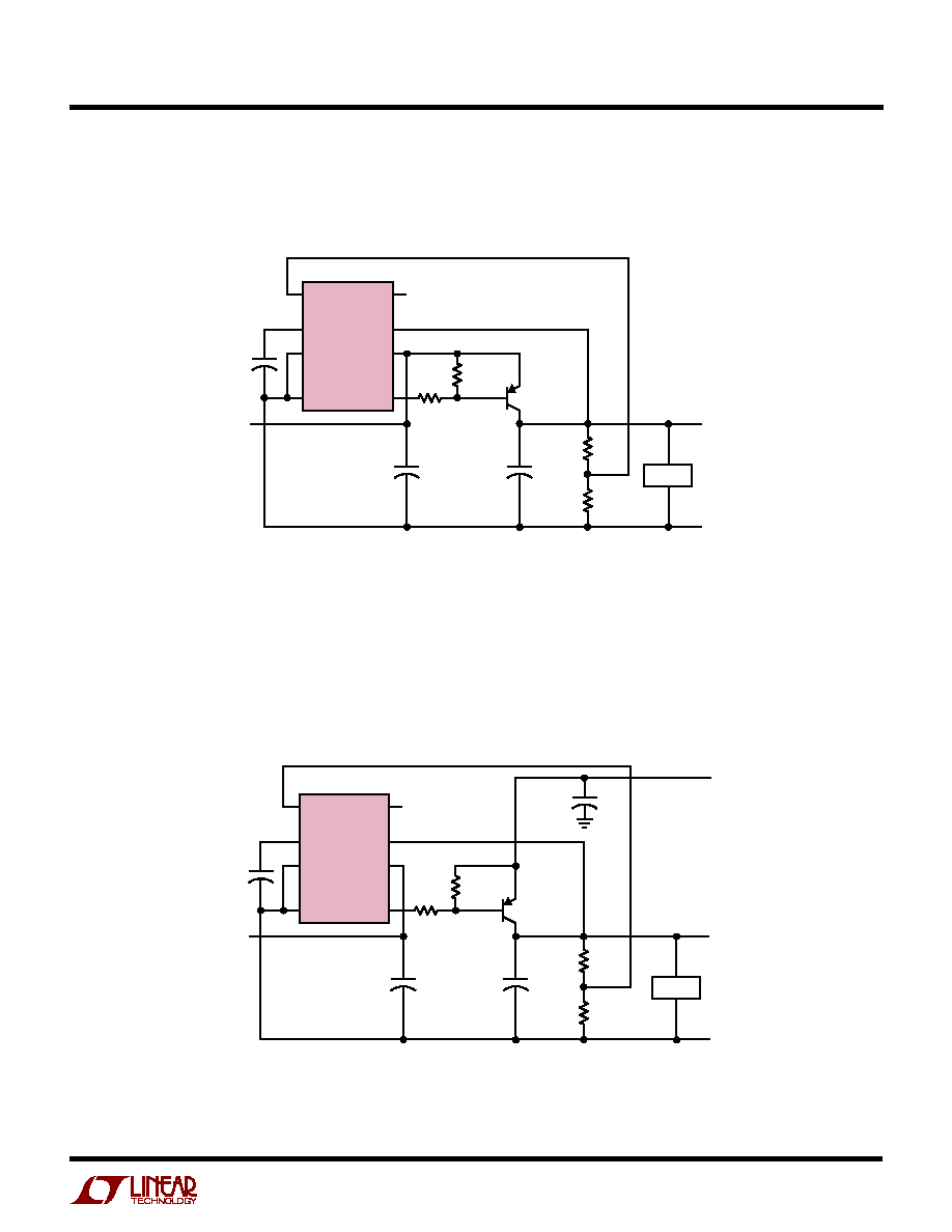
Basic Regulator Circuit
The basic regulator circuit is shown in Figure 2. The
adjustable output LT1573 senses the regulator output
voltage from its feedback pin via the output voltage
divider, R1 and R2, and drives the base of the external PNP
transistor to maintain the regulator output at the desired
value. For fixed output versions of the LT1573, the regu-
lator output voltage is sensed from the feedback pin via an
internal voltage divider. The resistor R
D
is required for the
overcurrent latch-off function. R
D
is also used to limit the
drive current available to the external PNP transistor and
to limit the power dissipation in the LT1573. Limiting the
drive current to the external PNP transistor will limit the
output current of the regulator which minimizes the stress
APPLICATIO S I FOR ATIO
W
U
U
U

8
LT1573
Current Limit
For regulator circuits using the LT1573, current limiting is
achieved by limiting the base drive current to the external
PNP pass transistor. This means that the actual system
current limit will be a function of both the current limit of
the LT1573 and the Beta of the external PNP. Motorola
provides the following Beta information for the D45H11.
The minimum Beta of the D45H11 is 60 when V
CE
= 1V and
I
C
= 2A. The minimum Beta is 40 when V
CE
= 1V and I
C
=
4A. For other PNP transistors, the user should first find out
the Beta information from the external PNP transistor
manufacturer to determine the appropriate LT1573 base
drive current limit. The current limit of the regulator
system then can be achieved by selecting the appropriate
amount of resistance R
D
in Figure 2.
Selecting R
D
Resistor R
D
can be used to limit the available drive current
to the external PNP transistor. In order to select R
D
, the
user should first choose the value of the drive current that
will give the required value of output current and dropout
voltage. For a circuit using the D45H11 as a pass transistor
this can be done using Table 1. For circuits using transis-
tors other than D45H11, the user must characterize the
transistor to determine the drive current requirements for
the specified output current and dropout voltage. In gen-
eral, it is recommended that the user choose the lowest
value of drive current that will satisfy the output current
requirements. This will minimize the stress on circuit
components during overload conditions.
The formula used to determine the resistor R
D
is:
R
D
= (V
IN
≠ V
BE
≠ V
DRIVE
)/(I
DRIVE
+ I
RB
)
(1)
where,
V
IN
= the minimum input voltage to the circuit
V
BE
= the maximum emitter/base voltage of the PNP
pass transistor
I
DRIVE
= the minimum PNP base current required
I
RB
= the current through R
B
= V
BE
/R
B
V
DRIVE
= the DRIVE pin saturation voltage when the DRIVE
pin current equals (I
DRIVE
+ I
RB
)
output current with dropout voltage as low as 0.35V. The
gain-bandwidth product f
T
of the D45H11 is typically
40MHz which enables the regulator, composed of this
PNP transistor and the LT1573, to handle the load changes
of several amps in a few hundred nanoseconds with a
minimum amount of output capacitance.
The following sections describe how specifications can be
determined for the basic regulator based on the LT1573
and D45H11 from Motorola. To determine the specifica-
tions for regulators formed by the LT1573 and other PNP
transistors, a similar method can be used.
Dropout Voltage
The dropout voltage of an LT1573-based regulator circuit
is determined by the V
CE
saturation voltage of the discrete
external PNP transistor when it is driven with a base
current equal to the available drive current of the LT1573.
The LT1573 is guaranteed to sink 250mA of base current
(440mA typ). The available drive current of the LT1573 can
be reduced by adding a resistor (R
D
in Figure 2) in series
with the DRIVE pin. Table 1 lists some useful operating
points for the D45H11. These points were empirically
determined using a sampling of devices.
Table 1. D45H11 Dropout Voltage
TYPICAL
DRIVE CURRENT
OUTPUT CURRENT
DROPOUT VOLTAGE
(mA)
(A)
(V)
20
1
0.20
20
2
0.50
40
2
0.25
40
3
0.50
60
3
0.25
60
4
0.70
80
4
0.45
100
4
0.35
100
5
0.70
150
5
0.40
200
5
0.35
150
6
0.65
200
6
0.45
250
7
0.50
APPLICATIO S I FOR ATIO
W
U
U
U

9
LT1573
Resistor R
B
helps to turn off the PNP (Q
OUT
in Figure 2).
Smaller values for R
B
turn off the PNP faster but will
increase input current. The recommended value for R
B
is
50
. For circuits that do not require high output current or
fast transient response, the value of R
B
can be increased
up to 200
. For the D45H11, the emitter-base voltage is
a function of base and collector current. Table 2 lists some
useful operating points for the D45H11. These points were
empirically determined using a sampling of devices.
Table 2. D45H11 V
BE
I
B
I
C
V
BE
AT 25
∞
C
(mA)
(A)
(V)
1
0.2
0.65
7
1
0.75
23
2
0.80
45
3
0.85
66
4
0.90
100
5
0.95
Design Example
Given the following operating requirements:
4.5V < V
IN
< 5.5V
I
OUT(MAX)
= 5A
V
OUT
= 3.3V
1. The first step is to determine the required drive current
for the D45H11. Dropout voltage must be less than 1.2V
at 5A output current. From Table 1, a drive current of
100mA will give 0.7V dropout voltage at an output
current of 5A. This satisfies the operating require-
ments.
2. The next step is to determine the value of R
D
. Assume
R
B
is 50
. From Table 2, the maximum emitter-base
voltage for this design is 0.95V. The current through
R
B
is:
I
RB
= V
BE
/R
B
= 0.95/50 = 19mA
V
DRIVE
is the DRIVE pin saturation voltage when the
DRIVE pin current equals 119mA, which can be read
from the typical performance characteristics curve to
be 0.39V. Resistor R
D
now can be calculated from
Eq (1):
R
D
= (4.5 ≠ 0.95 ≠ 0.39)V/(100 + 19)mA = 26.6
The next lowest 5% value is 24
.
Overcurrent Latch-Off
In addition to limiting the base drive current, the resistor
R
D
is included in the circuit for the overcurrent protection
latch-off function. There is a minimum value for this
resistance. It is calculated by Equation 1 with the drive
current I
DRIVE
set to the minimum available drive current
(= 250mA) from the LT1573. At high currents, R
D
also
limits the power dissipation in the LT1573. In some
conditions, resistor R
D
can be replaced with a short. This
is possible in circuits where an overload is unlikely and the
input voltage and drive requirements are low. If resistor R
D
is not included in the circuit, the regulator is protected
against the overcurrent condition only by the thermal
shutdown function. After the resistor R
D
is determined, a
certain amount of base drive current is available to the
external PNP transistor. An overcurrent or output short
condition will demand a base drive current greater than the
LT1573 can supply. The internal drive transistor will
saturate. A time-out latch will be triggered by this
overcurrent condition to turn off the regulator system. The
time-out period is determined by an external capacitor
connected between the LATCH and GND pins. The time-
out period is equal to the time it takes for the capacitor to
charge from 0V to the latch threshold which is equal to
2V
BE
. The latch charging current is set by an internal
current source and is a function of input voltage and
temperature as shown in the typical performance charac-
teristics curve. At 25
∞
C, the typical latch charging current
ranges from 7.2
µ
A with 3V input to 8
µ
A with 7V input. If
the overcurrent or output short condition persists longer
than the time-out period, the regulator will be shut down.
Otherwise, the regulator will function normally. In the
latch-off mode, some extra current is drawn from the input
to maintain the latch. The latching current is a function of
input voltage and temperature as shown in the typical
performance characteristic curve. At 25
∞
C, the typical
latching current ranges from 0.3mA with 3V input to
9.5mA with 7V input. The latch can be reset by recycling
input power, by grounding the LATCH pin or by putting the
device into shutdown.
APPLICATIO S I FOR ATIO
W
U
U
U

10
LT1573
Thermal Considerations
The thermal characteristics of several components need
to be considered; the LT1573, the pass transistor and
resistor R
D
. Power dissipation should be calculated based
on the worst-case conditions seen by each component
during normal operation.
1. Power Dissipation of the LT1573: The worst-case
power dissipation in the LT1573 is a function of drive
current, supply voltage and the value of R
D
. Worst-case
dissipation for the LT1573 occurs when the drive cur-
rent is equal to approximately one half of its maximum
value. The worst-case power dissipation in the LT1573
can be calculated by the following formula:
P
V
V
R
R
D
IN
BE
D
D
=
-
(
)
>
2
4
minimum R for latch - off function
D
(2)
where,
V
IN
= the maximum input voltage to the circuit
V
BE
= the minimum emitter/base voltage of the PNP
pass transistor
Following the previous design example for selecting
resistor R
D
, the power dissipation of LT1573 is calcu-
lated from Eq (2):
P
W
D
=
-
(
)
( )
=
5 5 0 65
4 24
0 25
2
.
.
.
For some operating conditions R
D
may be replaced with
a short. This is possible in applications where the
operating requirements (input voltage and drive cur-
rent) are at the low end and the output will not be
shorted. For R
D
= 0, the following formula may be used
to calculate the maximum power dissipation in the
LT1573:
P
D
= (V
IN
≠ V
BE
)(I
DRIVE
)
(3)
where,
V
IN
= the maximum input voltage
V
BE
= the minimum emitter/base voltage of the PNP
I
DRIVE
= the required maximum drive current
2. Power Dissipation of the Resistor R
D
: The worst-case
power dissipation in resistor R
D
needs to be calculated
so that the power rating of the resistor can be deter-
mined. The worst-case power dissipation in this resis-
tor will occur when the drive current is at a maximum.
The power dissipation can be calculated from the fol-
lowing formula:
P
V
V
V
R
RD
IN
BE
DRIVE
D
=
-
-
(
)
2
(4)
where,
V
IN
= the maximum input voltage
V
BE
= the minimum emitter/base voltage of the PNP
V
DRIVE
= the voltage at the LT1573 DRIVE pin
= V
SAT
of the DRIVE pin in the worst case
Following the previous design example, the power
dissipation of resistor R
D
is calculated from Eq (4):
P
W
RD
=
-
-
(
)
=
5 5 0 65 0 39
24
0 83
2
.
.
.
.
3. Power Dissipation of the PNP Transistor: The worst-
case power dissipation in the PNP pass transistor is
simply equal to:
P
PNP
= (V
IN
≠ V
OUT
)(I
OUT
)
(5)
where,
V
IN
= the maximum input voltage
I
OUT
= the maximum output current
Following the previous design example, the power
dissipation of PNP transistor is calculated from Eq (5):
P
PNP
= (5.5 ≠ 3.3)(5) = 11W
The LT1573 series regulators have internal thermal
limiting designed to protect the device during overload
conditions. For continuous normal load conditions,
the maximum junction temperature rating of 125
∞
C
must not be exceeded. It is important to give careful
consideration to all sources of thermal resistance from
junction to ambient. For surface mount devices, heat
sinking is accomplished by using the heat spreading
APPLICATIO S I FOR ATIO
W
U
U
U

11
LT1573
capabilities of the PC board and its copper traces. Table
3 lists some typical values for the thermal resistance of
the LT1573. Measured values of thermal resistance for
a specific board size with different copper areas are
listed. All measurements were taken in still air on 3/32
"
FR-4 board with 2oz copper. It is possible to achieve
significantly lower values with thinner multilayer boards.
Compensation
In order to improve the transient response to regulator
output load variation, a capacitor in series with a resistor
can be inserted between the V
OUT
and COMP pins. For the
microprocessor power supply regulator system based on
the LT1573 and the PNP transistor D45H11 with 24 1
µ
F
surface mount ceramic capacitors in parallel with one
220
µ
F surface mount tantalum capacitor at the output as
shown in Figure 1, a 100pF capacitor in series with a 1k
resistor is recommended. In theory, the output capacitor
forms the dominant pole of the regulator system. An
internal compensation capacitor forms another pole. The
external compensation capacitor and resistor form a zero
which adds phase margin to the regulator system to
prevent high frequency oscillation. The LT1573 has an
internal pole at approximately 5kHz. An external compen-
sation zero between 10kHz and 100kHz is usually required
to stabilize the regulator. The zero frequency is primarily
determined by the compensation capacitor and can be
roughly calculated by the following equation:
f
kHz
pF
C
pF
C
ZERO
COMP
COMP
=
( ) ( )( )
40
30
10
100
,
A compensation resistor between 1k and 10k is sug-
gested. A compensation resistor of 5k works for most
cases. In some cases, a greater compensation resistor is
needed to stop oscillation above 1MHz. In some cases, the
output capacitor may have enough equivalent series resis-
tance (ESR) to generate the required zero and the external
compensation zero may not be needed.
Output Capacitor
The LT1573 is designed to be used with an external PNP
transistor with a high gain-bandwidth product f
T
to make
a regulator with a very fast transient response, which can
minimize the size of the output capacitor. For a regulator
made of an LT1573 and a D45H11, only one 10
µ
F surface
mount ceramic capacitor at the output is enough for the
regulator to handle the output load varying up to 5A in a
few hundred nanoseconds interval and to remain stable
with a 30pF capacitor in series with a 7.5k resistor between
the V
OUT
and COMP pins. If tighter voltage regulation is
Table 3. LT1573 Thermal Resistance
COPPER AREA
THERMAL RESISTANCE
TOPSIDE*
BACKSIDE
BOARD AREA (JUNCTION-TO-AMBIENT)
2500mm
2
2500mm
2
2500mm
2
80
∞
C/W
1000mm
2
2500mm
2
2500mm
2
80
∞
C/W
225mm
2
2500mm
2
2500mm
2
85
∞
C/W
*Device is mounted on topside.
We can find out the maximum junction temperature of
the LT1573 during normal load operation after we
calculate the maximum power dissipation of the LT1573
from Eq (2). From the previous design example, the
maximum power dissipation of the LT1573 is 0.2W.
From Table 3, we know the thermal resistance from
junction-to-ambient is around 85
∞
C/W. The tempera-
ture difference between junction and ambient is:
(0.25W)(85
∞
C/W) = 21.25
∞
C
If the maximum ambient temperature is specified at
50
∞
C, the maximum junction temperature will be:
T
JMAX
= 50
∞
C + 21.25
∞
C = 71.25
∞
C
The maximum junction temperature must not exceed
the specified 125
∞
C for safe continuous regulator op-
eration.
Thermal Limiting
The thermal shutdown temperature of the LT1573 is
approximately 150
∞
C. The thermal limit of the LT1573 can
be used to protect both the LT1573 and the external PNP
pass transistor. This is accomplished by thermally cou-
pling the LT1573 to the PNP power transistor by locating
the LT1573 as close to the PNP transistor as possible. In
this case, the power dissipation of the power transistor
must be considered in the LT1573 maximum junction
temperature calculation.
APPLICATIO S I FOR ATIO
W
U
U
U

12
LT1573
needed during output transients, more capacitance can be
added to the regulator output. If more capacitance is
added to the output, the bandwidth of the regulator is
lowered. A large value compensation capacitor may be
needed to lower the frequency of the compensation zero to
avoid high frequency oscillation. Equal value output
capacitors with different ESR can have different output
transient response. High frequency performance will be
strongly affected by parasitics in the output capacitor and
board layout. Some experimentation with the external
compensation will be required for optimum results.
Shutdown Function
The regulator can be shut down by pulling the SHDN pin
voltage higher than the shutdown threshold (about 1.3V).
The regulator will restart itself if the SHDN is pulled below
the shutdown threshold.The SHDN pin should be tied to
ground if it is not used. The SHDN pin voltage can be
higher than the input voltage. When the SHDN pin voltage
is higher than 2V, the SHDN pin current increases and is
limited by a 20k resistor. Momentarily putting the device
into shutdown also resets the overcurrent latch.
Lower Dropout Voltage or Higher Output
Current Capability
Lower dropout voltage or higher output current capability
can be achieved by paralleling several output PNP transis-
tors as shown in Figure 3. By paralleling output PNP
transistors, the equivalent resistance between the emit-
ters (V
IN
) and collectors (V
OUT
) is lowered or each PNP
transistor sharing the output current now runs at a lower
collector current, which causes the dropout voltage to
decrease. Because the PNP transistors are running at a
lower collector current where the transistor beta is higher,
much more output current can be obtained at a given base
drive current. When paralleling two or more output tran-
sistors, a separate resistor is needed for R
B
and R
D
for
each output transistor. This allows the base drive current
to be split evenly between output transistors, which pro-
motes equal output current sharing. In the specific
example drawn in Figure 3 with two output transistors, the
resistance of R
B1
and R
B2
is now twice the value of the
resistance of R
B
in Figure 2, and the resistance of R
D1
and
R
D2
is twice the value of the resistance of R
D
in Figure 2.
In case of n PNP transistors in parallel, the resistance R
B
COMP
V
OUT
V
IN
DRIVE
FB
LATCH
SHDN
GND
LT1573
+
C
TIME
C
OUT1
C
C
V
IN
R
C
V
OUT
GND
1573 F03
R
B1
R
B2
R
D2
R
D1
R1
R2
LOAD
+
Q
OUT2
Q
OUT1
C
IN
Figure 3. Reduced Dropout Voltage or Increased Output Current
by Paralleling Output PNP Transistors
APPLICATIO S I FOR ATIO
W
U
U
U

13
LT1573
equals the resistance of R
B1
, R
B2
, ..., and R
Bn
in parallel,
and the resistance R
D
equals the resistance of R
D1
, R
D2
, ...,
and R
Dn
in parallel.
Voltage Feedback Resistor Divider Table
Voltage feedback resistor divider is provided for conve-
nience for the most possibly used output voltages in
Table 4.
Table 4. LT1573 Output Feedback Divider Resistance
OUTPUT
R1 (
)
VOLTAGE (V)
R2 (
)
(NEAREST 1%)
1.5
1k
187
1.8
1k
422
2.0
1k
576
2.2
1k
732
2.5
1k
976
2.8
1k
1210
3.0
1k
1370
3.3
1k
1620
3.5
1k
1780
3.8
1k
2000
4.0
1k
2150
4.5
1k
2550
5.0
1k
2940
COMP
V
OUT
FB
LATCH
LT1573
+
C
TIME
0.5
µ
F
C
OUT2
C
OUT1
C
C
100pF
V
IN
5V
R
C
1k
1/8W
R
D
24
1/2W
V
OUT
3.3V
GND
1573 TA01
R
B
50
1/8W
R1
1.6k
1/8W
R2
1k
1/8W
LOAD
+
+
Q
OUT
MOTOROLA
D45H11
C
OUT1
= 24
◊
1
µ
F SURFACE MOUNT CERAMIC CAPACITOR
(FOR T < 45
∞
C, C
OUT1
= 24
◊
1
µ
F Y5V CERAMIC SURFACE MOUNT CAPACITORS,
FOR T > 45
∞
C, C
OUT1
= 24
◊
1
µ
F X7R CERAMIC SURFACE MOUNT CAPACITORS)
PLACE C
OUT1
IN THE MICROPROCESSOR SOCKET CAVITY
C
IN
, C
OUT2
= 220
µ
F SURFACE MOUNT TANTALUM CAPACITOR
C
TIME
= 0.5
µ
F FOR 100ms TIME OUT AT ROOM TEMPERATURE
SHDN (ACTIVE HIGH) PIN SHOULD BE TIED TO GROUND IF IT IS NOT USED
C
IN
5V
V
IN
DRIVE
SHDN
GND
+
3.3V/5A Microprocessor Supply
APPLICATIO S I FOR ATIO
W
U
U
U
TYPICAL APPLICATIO S
U

14
LT1573
COMP
V
OUT
FB
LATCH
LT1573
+
C
TIME
0.5
µ
F
C
OUT
V
IN
6V to 9V
R
D
130
1/2W
V
OUT
5V
GND
1573 TA03
R
B
200
1/8W
R1
2.94k
1/8W
R2
1k
1/8W
LOAD
+
MOTOROLA
D45H11
C
IN
= 150
µ
F (SANYO SURFACE MOUNT ELECTROLYTIC, 10V, PART #10CV150BS)
OR 10
µ
F LOW ESR TANTALUM CAPACITOR
C
OUT
= 47
µ
F (SANYO SURFACE MOUNT ELECTROLYTIC, 25V, PART #25CV47BS)
OR 150
µ
F (SANYO SURFACE MOUNT ELECTROLYTIC, 10V, PART #10CV150BS)
C
TIME
= 0.5
µ
F FOR 100ms TIME OUT AT ROOM TEMPERATURE
SHDN (ACTIVE HIGH) PIN SHOULD BE TIED TO GROUND IF IT IS NOT USED
C
IN
V
IN
DRIVE
SHDN
GND
+
COMP
V
OUT
FB
LATCH
LT1573
+
C
TIME
0.5
µ
F
C
OUT2
C
OUT1
C
C
30pF
V
IN
3.3V
R
C
1k
1/8W
R
D
39
1/2W
V
OUT
2.5V
GND
1573 TA02
R
B
200
1/8W
R1
976
1/8W
R2
1k
1/8W
LOAD
+
+
Q
OUT
MOTOROLA
D45H11
C
IN
= 22
µ
F SURFACE MOUNT TANTALUM CAPACITOR
C
OUT1
= 10
µ
F SURFACE MOUNT CERAMIC CAPACITOR
C
OUT2
= 15
µ
F SURFACE MOUNT TANTALUM CAPACITOR
C
TIME
= 0.5
µ
F FOR 100ms TIME OUT AT ROOM TEMPERATURE
SHDN (ACTIVE HIGH) PIN SHOULD BE TIED TO GROUND IF IT IS NOT USED
C
IN
V
IN
DRIVE
SHDN
GND
+
3.3V to 2.5/2A Voltage Regulator
5V/2A Output from 6V to 9V Wall Adapter Input
TYPICAL APPLICATIO S
U
15
LT1573
Information furnished by Linear Technology Corporation is believed to be accurate and reliable.
However, no responsibility is assumed for its use. Linear Technology Corporation makes no represen-
tation that the interconnection of its circuits as described herein will not infringe on existing patent rights.
3.3V to 2.85V/1A Voltage Regulator
High Efficiency 2.5V to 1.5V Converter at 6A Output Current
COMP
V
OUT
FB
LATCH
LT1573
+
C
TIME
0.5
µ
F
C
OUT
V
IN
3.3V
R
D
91
1/2W
V
OUT
2.85V
GND
1573 TA04
R
B
200
1/8W
R1
1.24k
1/8W
R2
1k
1/8W
LOAD
+
MOTOROLA
D45H11
C
IN
,
C
OUT
= AVX 100
µ
F/10V SURFACE MOUNT TANTALUM CAPACITOR
C
TIME
= 0.5
µ
F FOR 100ms TIME OUT AT ROOM TEMPERATURE
SHDN (ACTIVE HIGH) PIN SHOULD BE TIED TO GROUND IF IT IS NOT USED
C
IN
V
IN
DRIVE
SHDN
GND
+
COMP
V
OUT
FB
LATCH
LT1573
+
C
TIME
0.5
µ
F
C
OUT
V
IN2
3V
TO 7V
R
D
6
1/2W
V
OUT
1.5V
V
IN1
2.5V
GND
1573 TA05
R
B
200
1/8W
R1
186
1/8W
R2
1k
1/8W
LOAD
MOTOROLA
D45H11
C
IN1
,
C
OUT
= AVX 100
µ
F/10V SURFACE MOUNT TANTALUM CAPACITOR
C
IN2
= AVX 15
µ
F/10V SURFACE MOUNT TANTALUM CAPACITOR
C
TIME
= 0.5
µ
F FOR 100ms TIME OUT AT ROOM TEMPERATURE
SHDN (ACTIVE HIGH) PIN SHOULD BE TIED TO GROUND IF IT IS NOT USED
C
IN2
V
IN
DRIVE
SHDN
GND
+
+
C
IN1
+
TYPICAL APPLICATIO S
U

16
LT1573
1573fa LT/TP 1299 2K REV A ∑ PRINTED IN USA
©
LINEAR TECHNOLOGY CORPORATION 1997
Linear Technology Corporation
1630 McCarthy Blvd., Milpitas, CA 95035-7417
q
(408) 432-1900
FAX: (408) 434-0507
q
TELEX: 499-3977
q
www.linear-tech.com
High Efficiency 2.5V to 1.8V Converter at 5A Output Current
COMP
V
OUT
FB
LATCH
LT1573
+
C
TIME
0.5
µ
F
C
OUT
V
IN2
3V
TO 7V
V
IN1
2.5V
V
OUT
1.8V
R
D
6.2
1/2W
GND
1573 TA06
R
B
200
1/8W
R1
420
1/8W
R2
1k
1/8W
LOAD
MOTOROLA
D45H11
C
IN1
, C
OUT
= AVX 100
µ
F/10V SURFACE MOUNT TANTALUM CAPACITOR
C
IN2
= AVX 15
µ
F/10V SURFACE MOUNT TANTALUM CAPACITOR
C
TIME
= 0.5
µ
F FOR 100ms TIME OUT AT ROOM TEMPERATURE
SHDN (ACTIVE HIGH) PIN SHOULD BE TIED TO GROUND IF IT IS NOT USED
C
IN2
V
IN
DRIVE
SHDN
GND
+
+
C
IN1
+
Dimensions in inches (millimeters) unless otherwise noted.
S8 Package
8-Lead Plastic Small Outline (Narrow 0.150)
(LTC DWG # 05-08-1610)
PART NUMBER
DESCRIPTION
COMMENTS
LT1529
3A Micropower Low Dropout Regulator
50
µ
A Quiescent Current, 0.5V Dropout, Shutdown
LT1575/LT1577
Low Dropout N-Channel MOSFET Regulator Driver
Ultrafast Transient, Adjustable/Fixed Output, Current Limiting
LT1580/LT1581
7A, 10A Very Low Dropout Linear Regulators
For High Current 3.3V to 2.xV Applications
LT1584/LT1585/LT1587
7A/4.6A/3A Low Dropout, Fast Response Regulators
For High Performance Microprocessors
LT1761/LT1762/LT1763
Low Noise LDO Micropower Regulators
20
µ
A to 30
µ
A Quiescent Current, 20
µ
V
RMS
Noise
LT1764
3A Fast Transient Response Low Dropout Regulator
340mV Dropout Voltage
RELATED PARTS
0.016 ≠ 0.050
(0.406 ≠ 1.270)
0.010 ≠ 0.020
(0.254 ≠ 0.508)
◊
45
∞
0
∞
≠ 8
∞
TYP
0.008 ≠ 0.010
(0.203 ≠ 0.254)
SO8 1298
0.053 ≠ 0.069
(1.346 ≠ 1.752)
0.014 ≠ 0.019
(0.355 ≠ 0.483)
TYP
0.004 ≠ 0.010
(0.101 ≠ 0.254)
0.050
(1.270)
BSC
1
2
3
4
0.150 ≠ 0.157**
(3.810 ≠ 3.988)
8
7
6
5
0.189 ≠ 0.197*
(4.801 ≠ 5.004)
0.228 ≠ 0.244
(5.791 ≠ 6.197)
DIMENSION DOES NOT INCLUDE MOLD FLASH. MOLD FLASH
SHALL NOT EXCEED 0.006" (0.152mm) PER SIDE
DIMENSION DOES NOT INCLUDE INTERLEAD FLASH. INTERLEAD
FLASH SHALL NOT EXCEED 0.010" (0.254mm) PER SIDE
*
**
TYPICAL APPLICATIO S
U
U
PACKAGE DESCRIPTIO