Äîêóìåíòàöèÿ è îïèñàíèÿ www.docs.chipfind.ru
1
LT1581/LT1581-2.5
s
Low Dropout, 430mV at 10A Output Current
s
Fast Transient Response
s
Remote Sense
s
1mV Load Regulation
s
Fixed 2.5V Output and Adjustable Output
s
No Supply Sequencing Problems in
Dual Supply Mode
The LT
®
1581 is a 10A low dropout regulator designed to
power the new generation of microprocessors. The drop-
out voltage of this device is 100mV at light loads rising to
just 430mV at 10A. To achieve this dropout a second low
current input voltage 1V greater than the output voltage is
required. The device can also be used as a single supply
device where dropout is comparable to an LT1584.
Several other new features have been added to the LT1581.
A remote SENSE pin is brought out. This feature virtually
eliminates output voltage variations due to load changes.
Typical load regulation for a load current step of 100mA to
10A, measured at the SENSE pin, is less than 1mV.
The LT1581 has fast transient response, equal to the
LT1584. On fixed voltage devices, the ADJUST pin is
brought out. A small capacitor on the ADJUST pin further
improves transient response.
This device is ideal for generating processor supplies of
2V to 3V on motherboards where both 5V and 3.3V
supplies are available.
10A, Very Low
Dropout Regulators
FEATURES
DESCRIPTIO
N
U
, LTC and LT are registered trademarks of Linear Technology Corporation.
Pentium is a registered trademark of Intel Corporation.
PowerPC is a trademark of IBM Corporation.
APPLICATIO
N
S
U
s
Microprocessor Supplies
s
Post Regulators for Switching Supplies
s
High Current Regulators
s
5V to 3.XXV for Pentium
®
Processors Operating
at 90MHz to 166MHz and Beyond
s
3.3V to 2.9V for Portable Pentium Processor
s
PowerPC
TM
Series Power Supplies
Dropout Voltage
Minimum Power Voltage
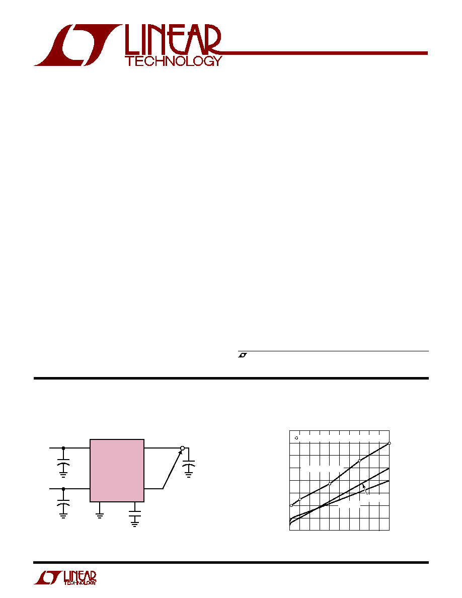
TYPICAL APPLICATIO
N
U
OUTPUT
SENSE
ADJ
GND
0.1
µ
F
1581 TA01
10
µ
F
TANT
330
µ
F
OS-CON
2.5V/10A
LT1581-2.5
100
µ
F TANT
AVX TPS
×
7
POWER
3.3V
10A
5V
0.2A
CONTROL
+
+
+
2.5V Microprocessor Supply
OUTPUT CURRENT (A)
MINIMUM POWER VOLTAGE (V)
(V
POWER
V
OUT
) (V)
0.8
0.7
0.6
0.5
0.4
0.3
0.2
0.1
0
1581 G03
0
1
5
7
4
2
3
6
8
10
9
DATA SHEET LIMIT
T
J
= 25
°
C
T
J
= 125
°
C
INDICATES GUARANTEED TEST POINTS
2
LT1581/LT1581-2.5
ABSOLUTE
M
AXI
M
U
M
RATINGS
W
W
W
U
PACKAGE/ORDER I
N
FOR
M
ATIO
N
W
U
U
ELECTRICAL CHARACTERISTICS
PRECO
N
DITIO
N
I
N
G
U
U
U
100% Thermal Limit Functional Test
Consult factory for Industrial and Military grade parts.
LT1581CT7
LT1581CT7-2.5
ORDER PART
NUMBER
(Note 1)
V
POWER
Input Voltage ................................................ 6V
V
CONTROL
Input Voltage ........................................... 13V
Operating Junction Temperature Range
Control Section ...................................... 0
°
C to 125
°
C
Power Transistor ................................... 0
°
C to 150
°
C
Storage Temperature ............................ 65
°
C to 150
°
C
Lead Temperature (Soldering, 10 sec) .................. 300
°
C
*PIN2 = NC FOR LT1581CT7, GND FOR LT1581CT7-2.5
T7 PACKAGE
7-LEAD PLASTIC TO-220
FRONT VIEW
TAB IS
OUTPUT
NC
V
CONTROL
V
POWER
OUTPUT
SENSE
NC/GND*
ADJUST
7
6
5
4
3
2
1
JA
= 50
°
C/ W
The
q
denotes specifications which apply over the full operating
temperature range, otherwise specifications are at T
A
= 25
°
C. (Note 2)
PARAMETER
CONDITIONS
MIN
TYP
MAX
UNITS
Output Voltage:
LT1581-2.5
V
CONTROL
= 5V, V
POWER
= 3.3V, I
LOAD
= 0mA
2.485
2.500
2.515
V
V
CONTROL
= 4V to 12V, V
POWER
= 3V to 5.5V, I
LOAD
= 0mA to 4A
q
2.475
2.500
2.525
V
V
CONTROL
= 4V to 12V, V
POWER
= 3.3V to 5.5V, I
LOAD
= 0mA to 10A
q
2.475
2.500
2.525
V
Reference Voltage:
LT1581
V
CONTROL
= 2.75V, V
POWER
= 2V, I
LOAD
= 10mA
1.243
1.250
1.257
V
(V
ADJ
= 0V)
V
CONTROL
= 2.7V to 12V, V
POWER
= 1.75V to 5.5V, I
LOAD
= 0mA to 4A
q
1.237
1.250
1.263
V
V
CONTROL
= 2.7V to 12V, V
POWER
= 2.05V to 5.5V, I
LOAD
= 0mA to 10A
q
1.237
1.250
1.263
V
Line Regulation: LT1581-2.5
V
CONTROL
= 3.65V to 12V, V
POWER
= 3V to 5.5V, I
LOAD
= 10mA
q
1
3
mV
LT1581
V
CONTROL
= 2.5V to 12V, V
POWER
= 1.75V to 5.5V, I
LOAD
= 10mA
q
1
3
mV
Load Regulation: LT1581-2.5
V
CONTROL
= 5V, V
POWER
= 3.3V, I
LOAD
= 0mA to 10A
q
1
10
mV
LT1581 (V
ADJ
= 0V)
V
CONTROL
= 2.75V, V
POWER
= 2.1V, I
LOAD
= 10mA to 10A
q
1
5
mV
Minimum Load Current: LT1581
V
CONTROL
= 5V, V
POWER
= 3.3V, V
ADJ
= 0V (Note 4)
q
3
10
mA
Control Pin Current: LT1581-2.5
V
CONTROL
= 5V, V
POWER
= 3.3V, I
LOAD
= 100mA
q
5
10
mA
(Note 5)
V
CONTROL
= 5V, V
POWER
= 3.3V, I
LOAD
= 4A
q
20
50
mA
V
CONTROL
= 5V, V
POWER
= 3.3V, I
LOAD
= 7A
q
40
100
mA
V
CONTROL
= 5V, V
POWER
= 3.3V, I
LOAD
= 10A
q
70
170
mA
Control Pin Current: LT1581
V
CONTROL
= 2.75V, V
POWER
= 2.05V, I
LOAD
= 100mA
q
5
10
mA
(Note 5)
V
CONTROL
= 2.75V, V
POWER
= 2.05V, I
LOAD
= 4A
q
20
50
mA
V
CONTROL
= 2.75V, V
POWER
= 2.05V, I
LOAD
= 7A
q
40
100
mA
V
CONTROL
= 2.75V, V
POWER
= 2.05V, I
LOAD
= 10A
q
70
170
mA
Ground Pin Current: LT1581-2.5
V
CONTROL
= 5V, V
POWER
= 3.3V, I
LOAD
= 0mA
q
6
10
mA
Adjust Pin Current: LT1581 (V
ADJ
= 0V) V
CONTROL
= 2.75V, V
POWER
= 2.05V, I
LOAD
= 10mA
q
60
120
µ
A
Current Limit:
LT1581-2.5
V
CONTROL
= 5V, V
POWER
= 3.3V,
V
OUT
= 100mV
q
10.1
11
A
LT1581 (V
ADJ
= 0V)
V
CONTROL
= 2.75V, V
POWER
= 2.05V,
V
OUT
= 100mV
q
10.1
11
A
Ripple Rejection: LT1581-2.5
V
CONTROL
= V
POWER
= 5V Avg, V
RIPPLE
= 1V
P-P
, f
RIPPLE
= 120Hz,
55
80
dB
I
OUT
= 4A, T
J
= 25
°
C
LT1581
V
CONTROL
= V
POWER
= 3.75V Avg, V
RIPPLE
= 1V
P-P
, f
RIPPLE
= 120Hz,
60
80
dB
V
ADJ
= 0V, I
OUT
= 4A, T
J
= 25
°
C
Thermal Regulation
30ms Pulse
0.004
0.020
%/W
Thermal Resistance, Junction-to-Case
Control Circuitry/Power Transistor
0.65/2.50
°
C/W
3
LT1581/LT1581-2.5
ELECTRICAL CHARACTERISTICS
The
q
denotes specifications which apply over the full operating
temperature range, otherwise specifications are at T
A
= 25
°
C. (Note 2)
PARAMETER
CONDITIONS
MIN
TYP
MAX
UNITS
Dropout Voltage (Note 3)
Minimum V
CONTROL
: LT1581-2.5
V
POWER
= 3.3V, I
LOAD
= 100mA
q
1.02
1.25
V
(V
CONTROL
V
OUT
)
V
POWER
= 3.3V, I
LOAD
= 1A
q
1.04
1.27
V
V
POWER
= 3.3V, I
LOAD
= 4A
q
1.06
1.30
V
V
POWER
= 3.3V, I
LOAD
= 7A
q
1.10
1.33
V
V
POWER
= 3.3V, I
LOAD
= 10A
q
1.12
1.35
V
Minimum V
CONTROL
: LT1581
V
POWER
= 2.05V, I
LOAD
= 100mA
q
1.02
1.25
V
(V
CONTROL
V
OUT
)
V
POWER
= 2.05V, I
LOAD
= 1A
q
1.04
1.27
V
(V
ADJ
= 0V)
V
POWER
= 2.05V, I
LOAD
= 4A
q
1.06
1.30
V
V
POWER
= 2.05V, I
LOAD
= 7A
q
1.10
1.33
V
V
POWER
= 2.05V, I
LOAD
= 10A
q
1.12
1.35
V
Minimum V
POWER
:
LT1581-2.5
V
CONTROL
= 5V, I
LOAD
= 100mA
q
0.10
0.20
V
(V
POWER
V
OUT
)
V
CONTROL
= 5V, I
LOAD
= 1A
q
0.13
0.25
V
V
CONTROL
= 5V, I
LOAD
= 4A, T
J
= 25
°
C
0.22
0.33
V
V
CONTROL
= 5V, I
LOAD
= 4A
q
0.37
V
V
CONTROL
= 5V, I
LOAD
= 7A, T
J
= 25
°
C
0.31
0.45
V
V
CONTROL
= 5V, I
LOAD
= 7A
q
0.55
V
V
CONTROL
= 5V, I
LOAD
= 10A, T
J
= 25
°
C
0.43
0.63
V
V
CONTROL
= 5V, I
LOAD
= 10A
q
0.70
V
Minimum V
POWER
:
LT1581
V
CONTROL
= 2.75V, I
LOAD
= 100mA
q
0.10
0.20
V
(V
POWER
V
OUT
)
V
CONTROL
= 2.75V, I
LOAD
= 1A
q
0.13
0.25
V
(V
ADJ
= 0V)
V
CONTROL
= 2.75V, I
LOAD
= 4A, T
J
= 25
°
C
0.22
0.33
V
V
CONTROL
= 2.75V, I
LOAD
= 4A
q
0.37
V
V
CONTROL
= 2.75V, I
LOAD
= 7A, T
J
= 25
°
C
0.31
0.45
V
V
CONTROL
= 2.75V, I
LOAD
= 7A
q
0.55
V
V
CONTROL
= 2.75V, I
LOAD
= 10A, T
J
= 25
°
C
0.43
0.63
V
V
CONTROL
= 2.75V, I
LOAD
= 10A
q
0.70
V
Note 1: Absolute Maximum Ratings are those values beyond which the life
of a device may be impaired.
Note 2: Unless otherwise specified, V
OUT
= V
SENSE
. For the LT1581
adjustable device, V
ADJ
= 0V.
Note 3: For the LT1581, dropout is caused by either minimum control
voltage (V
CONTROL
) or minimum power voltage (V
POWER
). Both parameters
are specified with respect to the output voltage. The specifications represent
the minimum input-to-output voltage required to maintain 1% regulation.
Note 4: For the LT1581 adjustable device the minimum load current is the
minimum current required to maintain regulation. Normally, the current in
the resistor divider used to set the output voltage is selected to meet the
minimum load current requirement.
Note 5: The CONTROL pin current is the drive current required for the
output transistor. This current will track output current with roughly a
1:100 ratio. The minimum value is equal to the quiescent current of the
device.
4
LT1581/LT1581-2.5
TYPICAL PERFOR
M
A
N
CE CHARACTERISTICS
U
W
PI
N
FU
N
CTIO
N
S
U
U
U
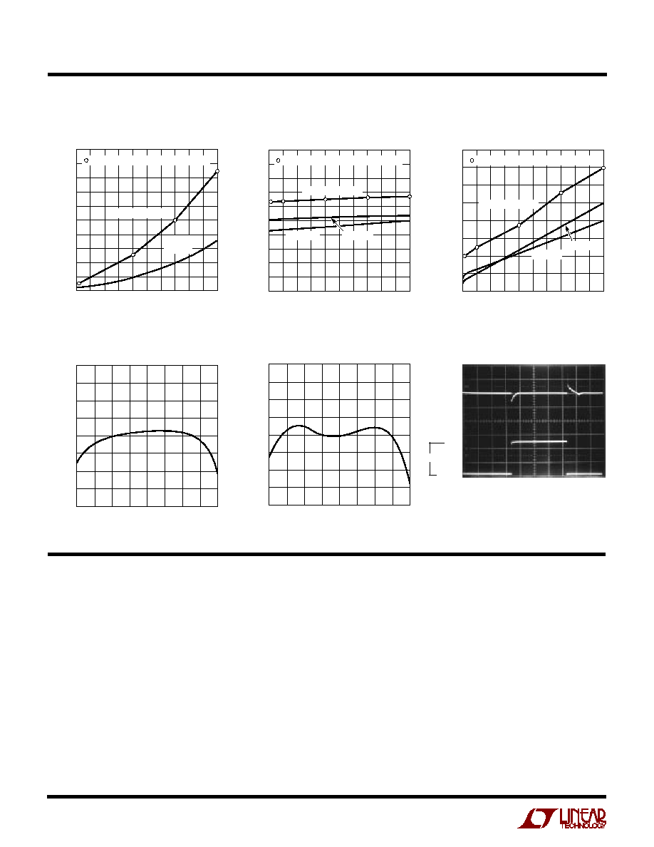
OUTPUT CURRENT (A)
0
MINIMUM CONTROL VOLTAGE
(V
CONTROL
V
OUT
) (V)
2
0
1
5
7
1581 G02
4
2
3
6
8
10
9
1
INDICATES GUARANTEED TEST POINTS
DATA SHEET LIMIT
T
J
= 25
°
C
T
J
= 125
°
C
TEMPERATURE (
°
C)
50 25
OUTPUT VOLTAGE (V)
150
1581 G05
0
25
75
125
50
100
2.512
2.509
2.506
2.503
2.500
2.497
2.494
2.491
2.488
TEMPERATURE (
°
C)
50 25
REFERENCE VOLTAGE (V)
150
1581 G04
0
25
75
125
50
100
1.262
1.259
1.256
1.253
1.250
1.247
1.244
1.241
1.238
LT1581 Reference Voltage vs
Temperature
Control Pin Current vs
Output Current
400mA
LT1581-2.5 Output Voltage vs
Temperature
V
OUT
50mV/DIV
50
µ
s/DIV
1581 G06
Load Current Step Response
ADJUST (Pin 1): This pin is the negative side of the
reference voltage for the device. Transient response can
be improved by adding a small bypass capacitor from the
ADJUST pin to ground. For fixed voltage devices the
ADJUST pin is also brought out to allow the user to add a
bypass capacitor.
GND (Pin 2, Fixed Voltage Devices Only): For fixed
voltage devices this is the bottom of the resistor divider
that sets the output voltage.
SENSE (Pin 3): This pin is the positive side of the reference
voltage for the device. With this pin it is possible to Kelvin
sense the output voltage at the load.
OUTPUT (Pin 4): This is the power output of the device.
V
POWER
(Pin 5): This is the collector to the power device
of the LT1581. The output load current is supplied through
this pin. For the device to regulate, the voltage at this pin
must be between 0.1V and 0.7V greater than the output
voltage (see Dropout specifications).
V
CONTROL
(Pin 6): This pin is the supply pin for the control
circuitry of the device. The current flow into this pin will
be about 1% of the output current. For the device to
regulate, the voltage at this pin must be between 1.0V and
1.35V greater than the output voltage (see Dropout
specifications).
Dropout Voltage --
Minimum Control Voltage
10A
LOAD
OUTPUT CURRENT (A)
MINIMUM POWER VOLTAGE (V)
(V
POWER
V
OUT
) (V)
0.8
0.7
0.6
0.5
0.4
0.3
0.2
0.1
0
1581 G03
0
1
5
7
4
2
3
6
8
10
9
DATA SHEET LIMIT
T
J
= 25
°
C
T
J
= 125
°
C
INDICATES GUARANTEED TEST POINTS
Dropout Voltage --
Minimum Power Voltage
OUTPUT CURRENT (A)
0
200
180
160
140
120
100
80
60
40
20
0
3
5
1581 G01
1
2
4
6
7
8
9
10
CONTROL PIN CURRENT (mA)
DATA SHEET LIMIT
INDICATES GUARANTEED TEST POINTS
TYPICAL
DEVICE
5
LT1581/LT1581-2.5
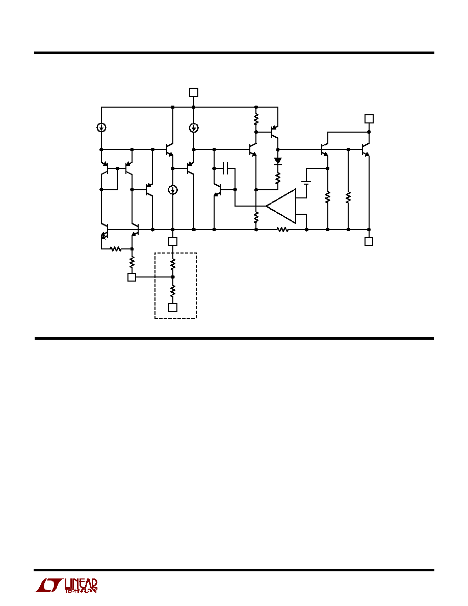
BLOCK DIAGRA
W
APPLICATIO
N
S I
N
FOR
M
ATIO
N
W
U
U
U
The LT1581 is a low dropout regulator designed to power
the new generation of microprocessors. Low dropout
regulators have become more common in desktop com-
puter systems as microprocessor manufacturers have
moved away from 5V only CPUs. A wide range of supply
requirements exists today with new voltages just over the
horizon. In many cases the input/output differential is very
small, effectively disqualifying many of the low dropout
regulators on the market today. The LT1581 is designed to
make use of multiple power supplies present in most
systems to reduce the dropout voltage. This 2-supply
approach maximizes efficiency.
The second supply, at least 1V greater than the output
voltage, is used to provide power for the control circuitry
and supply the drive current to the NPN output transistor.
This allows the NPN to be driven into saturation, thereby
reducing the dropout voltage by a V
BE
compared to
conventional designs. The current requirement for the
+
POWER
CONTROL
SENSE
OUTPUT
1581 BD
FOR FIXED
VOLTAGE
DEVICE
GND
ADJ
control voltage is relatively small, equal to approximately
1% of the output current or about 100mA for a 10A load.
The bulk of this current is drive current for the NPN output
transistor. This drive current becomes part of the output
current.
The control voltage must be at least 1V greater than the
output voltage to obtain optimum performance. The maxi-
mum voltage on the V
CONTROL
pin is 13V. The maximum
voltage at the V
POWER
pin is limited to 7V. GND pin current
for fixed voltage devices is 6mA (typ) and is constant as a
function of load. ADJUST pin current for adjustable de-
vices is 60
µ
A at 25
°
C and varies proportional to absolute
temperature.
The LT1581 has improved frequency compensation which
permits the use of capacitors with very low ESR. This is
critical in addressing the needs of modern, low voltage,
high speed microprocessors. Current generation micro-

6
LT1581/LT1581-2.5
APPLICATIO
N
S I
N
FOR
M
ATIO
N
W
U
U
U
processors cycle load current from several hundred mil-
liamperes to several amperes in tens of nanoseconds.
Output voltage tolerances are tighter and include transient
response as part of the specification. The LT1581 is
designed to meet the fast current load step requirements
of these microprocessors and saves total cost by needing
less output capacitance to maintain regulation.
Careful design has eliminated any supply sequencing
issues associated with a dual supply system. The output
voltage will not turn on until both supplies are operating.
If the control voltage comes up first, the output current will
be limited to a few milliamperes until the power input
voltage comes up. If the power input comes up first the
output will not turn on at all until the control voltage comes
up. The output can never come up unregulated. The
LT1581 can also be operated as a single supply device by
tying the control and power inputs together. Dropout in
single supply operation will be determined by the mini-
mum control voltage.
The LT1581 includes several innovative features that
require additional pins over the traditional 3-terminal
regulator. Both the fixed and adjustable devices have
remote sense pins, permitting very accurate regulation of
output voltage at the load, where it counts, rather than at
the regulator. As a result the typical load regulation over
an output current range of 100mA to 10A with a 2.5V
output is typically less than 1mV. For the fixed voltage
devices the ADJUST pin is also brought out. This allows
the user to improve transient response by bypassing the
internal resistor divider. In the past, fixed output voltage
devices did not provide this capability. Bypassing the
ADJUST pin with a capacitor in the range of 0.1
µ
F to 1
µ
F
will provide optimum transient response. The value cho-
sen will depend on the amount of output capacitance in the
system.
In addition to the enhancements mentioned above, the
reference accuracy has been improved by a factor of two
with a guaranteed initial tolerance of
±
0.6% at 25
°
C.
Temperature drift is also very well controlled. When com-
bined with ratiometrically accurate internal divider resis-
tors the part can easily hold 1% output accuracy over the
full temperature range and load current range, guaran-
teed, while operating with an input/output differential of
well under 1V.
Typical applications for the LT1581 include 3.3V to 2.5V
conversion with a 5V control supply, 5V to 4.2V conver-
sion with a 12V control supply or 5V to 3.6V conversion
with a 12V control supply. It is easy to obtain dropout
voltages of less than 0.4V at 4A along with excellent static
and dynamic specifications. The LT1581 is capable of 10A
of output current with a maximum dropout of 0.7V. The
LT1581 has fast transient response that allows it to handle
the large current changes associated with today's micro-
processors. The device is fully protected against overcurrent
and overtemperature conditions. Both fixed voltage (2.5V)
and adjustable output versions are available. The device is
available in a 7-lead TO-220 package.
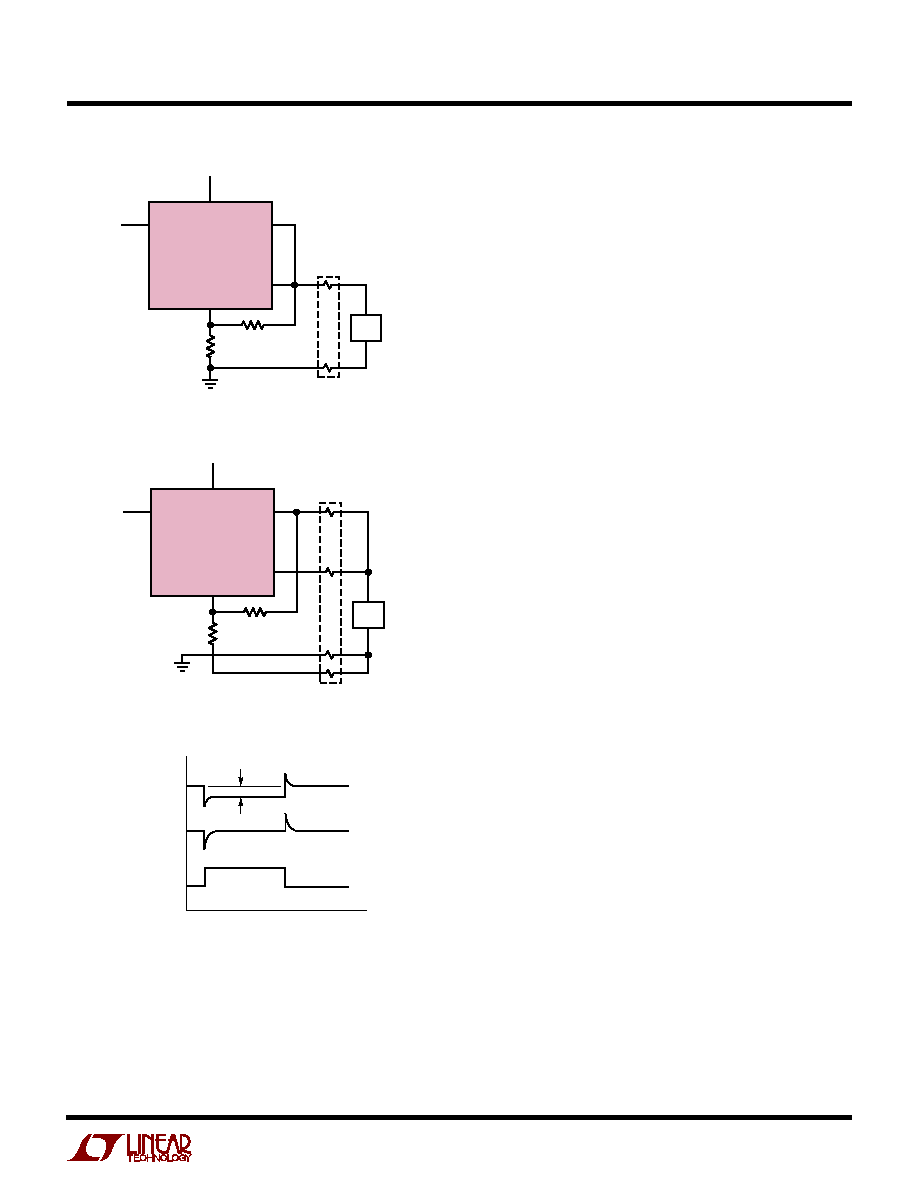
Grounding and Output Sensing
The LT1581 allows true Kelvin sensing for both the high
and low side of the load. This means that the voltage
regulation at the load can be easily optimized. Voltage
drops due to parasitic resistances between the regulator
and the load which would normally degrade regulation can
be placed inside the regulation loop of the LT1581. Figures
1 through 3 illustrate the advantages of remote sensing.
Figure 1 shows the LT1581 connected as a conventional
3-terminal regulator with the SENSE lead connected di-
rectly to the output of the device. R
P
represents the
parasitic resistance of the connections between the LT1581
and the load. The load is typically a microprocessor and
R
P
is made up of the PC traces and/or connector resis-
tances, in the case of a modular regulator, between the
regulator and the processor. The effect of R
P
can be seen
in trace A of Figure 3. Very small resistances cause
significant load regulation steps. For example, at 10A
output current the output voltage will shift by 10mV for
every 0.001
of resistance. In Figure 2 the LT1581 is
connected to take advantage of the remote sense feature.
The SENSE pin and the top of the resistor divider are
connected to the top of the load. The bottom of the resistor
divider is connected to the bottom of the load. R
P
is now
effectively connected inside the regulating loop of the
LT1581 and the load regulation at the load will be negli-
gible for reasonable values of R
P
. Trace B of Figure 3
7
LT1581/LT1581-2.5
APPLICATIO
N
S I
N
FOR
M
ATIO
N
W
U
U
U
OUTPUT
SENSE
ADJ
R2
R1
1581 F01
R
P
R
P
LT1581
POWER
3.3V
5V
CONTROL
LOAD
V
OUT
+
LT1581 can control the voltage at the load as long as the
input/output voltage is greater than the total of the dropout
voltage of the LT1581 plus the voltage drop across R
P
.
Stability
The LT1581 requires the use of an output capacitor as part
of the device frequency compensation. The device re-
quires a minimum of 22
µ
F tantalum or 150
µ
F of aluminum
electrolytic to ensure stability. Larger capacitor values
increase stability and improve transient performance.
Many different types of capacitors are available and have
widely varying characteristics. These capacitors differ in
capacitor tolerance (sometimes up to
±
100%), equivalent
series resistance, equivalent series inductance and ca-
pacitance temperature coefficient. The LT1581 frequency
compensation optimizes frequency response with low
ESR capacitors. In general, use capacitors with an ESR of
less than 1
.
For microprocessor applications larger value capacitors
will be needed to meet the transient requirements of the
processor. Processor manufacturers require tight voltage
tolerances on the power supply. High quality bypass
capacitors must be used to limit the high frequency noise
generated by the processor. Multiple small ceramic ca-
pacitors in addition to high quality bulk tantalum capaci-
tors are typically required to limit parasitic inductance
(ESL) and resistance (ESR) in the capacitors to acceptable
levels. The LT1581 is stable with the type of capacitors
recommended by processor manufacturers.
Bypassing the adjust terminal on the LT1581 improves
ripple rejection and transient response. The ADJUST pin is
brought out on the fixed voltage device specifically to
allow this capability.
Capacitor values on the order of several hundred microfar-
ads are used to ensure good transient response with heavy
load current changes. Output capacitance can increase
without limit and larger values of output capacitance
further improve the stability and transient response of the
LT1581.
Modern microprocessors generate large high frequency
current transients. The load current step contains higher
order frequency components that the output coupling
Figure 3. Remote Sensing Improves Load Regulation
Figure 2. Remote Load Sensing
Figure 1. Conventional Load Sensing
OUTPUT
SENSE
ADJ
R2
R1
1581 F02
R
P
R
P
LT1581
POWER
3.3V
5V
CONTROL
LOAD
V
OUT
+
V
OUT
FIGURE 1
(
I
OUT
)(R
P
)
TIME
1581 F03
V
OUT
FIGURE 2
I
OUT
illustrates the effect on output regulation. It is important to
note that the voltage drops due to R
P
are not eliminated.
They will add to the dropout voltage of the regulator
regardless of whether they are inside the loop as in Figure
2 or outside the loop as in Figure 1. This means that the
8
LT1581/LT1581-2.5
APPLICATIO
N
S I
N
FOR
M
ATIO
N
W
U
U
U
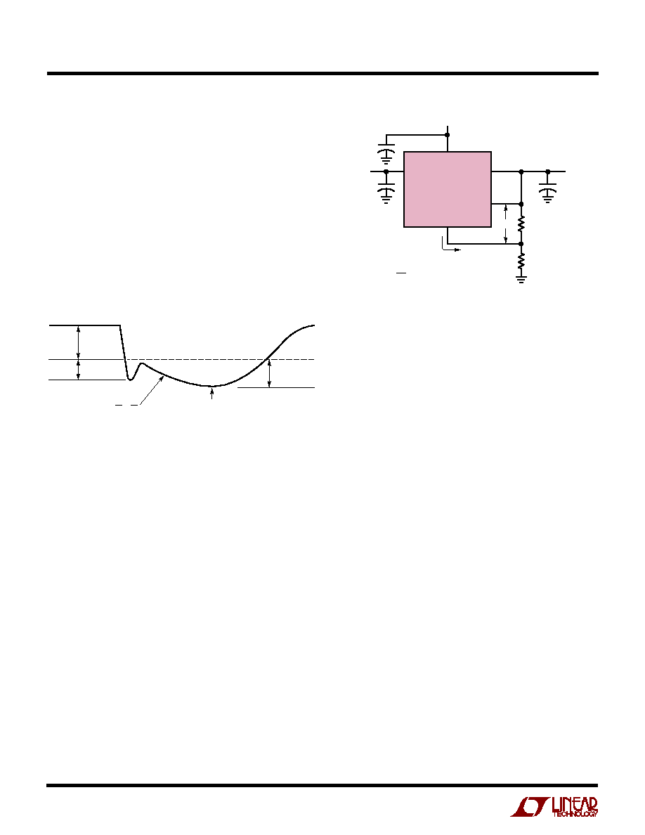
network must handle until the regulator throttles to the
load current level. Capacitors are not ideal elements and
contain parasitic resistance and inductance. These para-
sitic elements dominate the change in output voltage at
the beginning of a transient load step change. The ESR of
the output capacitors produces an instantaneous step in
output voltage (
V =
I)(ESR). The ESL of the output
capacitors produces a droop proportional to the rate of
change of the output current (V = L)(
I/
t). The output
capacitance produces a change in output voltage
proportional to the time until the regulator can respond
(
V =
t)(
I/C). These transient effects are illustrated in
Figure 4 .
ESR
EFFECTS
1581 F04
ESL
EFFECTS
CAPACITANCE
EFFECTS
POINT AT WHICH REGULATOR
TAKES CONTROL
SLOPE,
=
V
t
I
C
The use of capacitors with low ESR, low ESL and good
high frequency characteristics is critical in meeting the
output voltage tolerances of these high speed micropro-
cessors. These requirements dictate a combination of
high quality, surface mount, tantalum and ceramic capaci-
tors. The location of the decoupling network is critical to
transient performance. Place the decoupling network as
close to the processor pins as possible because trace runs
from the decoupling capacitors to the processor pins are
inductive. The ideal location for the decoupling network is
actually inside the microprocessor socket cavity. In addi-
tion, use large power and ground plane areas to minimize
distribution drops.
Output Voltage
The adjustable version of the LT1581 develops a 1.25V
reference voltage between the SENSE pin and the ADJUST
pin (see Figure 5). Placing a resistor R1 between these two
terminals causes a constant current to flow through R1
and down through R2 to set the overall output voltage.
Normally, R1 is chosen so that this current is the specified
Figure 4
OUTPUT
SENSE
ADJ
R2
I
ADJ
= 60
µ
A
1581 F05
LT1581
POWER
V
POWER
V
CONTROL
V
REF
CONTROL
R1
V
OUT
V
OUT
= V
REF
1 + + I
ADJ
(R2)
R2
R1
( )
+
+
+
minimum load current of 10mA. The current out of the
ADJUST pin adds to the current from R1. The ADJUST pin
current is small, typically 60
µ
A. The output voltage contri-
bution of the ADJUST pin current is small and only needs
to be considered when very precise output voltage setting
is required. Note that the top of the resistor divider should
be connected directly to the SENSE pin for best regulation.
See the section on grounding and Kelvin sensing above.
Protection Diodes
In normal operation the LT1581 does not require protec-
tion diodes. Older 3-terminal regulators require protection
diodes between the OUTPUT pin and the INPUT pin or
between the ADJUST pin and the OUTPUT pin to prevent
die overstress.
On the LT1581, internal resistors limit internal current
paths on the ADJUST pin. Therefore even with bypass
capacitors on the ADJUST pin, no protection diode is
needed to ensure device safety under short-circuit con-
ditions. The ADJUST pin can be driven on a transient
basis
±
7V with respect to the output without any device
degradation.
A protection diode between the OUTPUT pin and the
V
POWER
pin is usually not needed. An internal diode
between the OUTPUT pin and the V
POWER
pin on the
LT1581 can handle microsecond surge currents of 50A to
100A. Even with large value output capacitors it is difficult
to obtain those values of surge currents in normal opera-
tion. Only with large values of output capacitance, such as
Figure 5. Setting Output Voltage
9
LT1581/LT1581-2.5
Thermal Considerations
The LT1581 has internal current and thermal limiting
designed to protect the device under overload conditions.
For continuous normal load conditions maximum junction
temperature ratings must not be exceeded. It is important
to give careful consideration to all sources of thermal
resistance from junction to ambient. This includes junc-
tion-to-case, case-to-heat sink interface and heat sink
resistance itself. Thermal resistance specifications are
given in the electrical characteristics for both the Control
section and the Power section of the device. The thermal
resistance of the Control section is given as 0.65
°
C/W and
junction temperature of the Control section is allowed to
run at up to 125
°
C. The thermal resistance of the Power
section is given as 2.5
°
C/W and the junction temperature
of the Power section is allowed to run at up to 150
°
C. The
difference in thermal resistances between Control and
Power sections is due to thermal gradients between the
power transistor and the control circuitry.
Virtually all of the power dissipated by the device is
dissipated in the power transistor. The temperature rise in
the power transistor will be greater than the temperature
rise in the Control section so the effective thermal resis-
tance, temperature rise per watt dissipated, will be lower
in the Control section. At power levels below 12W the
temperature gradient will be less than 25
°
C and the
maximum ambient temperature will be determined by the
junction temperature of the Control section. This is due to
the lower maximum junction temperature in the Control
section. At power levels greater than 12W the temperature
gradient will be greater than 25
°
C and the maximum
ambient temperature will be determined by the Power
section. For both cases the junction temperature is deter-
mined by the total power dissipated in the device. For most
low dropout applications the power dissipation will be less
than 12W.
The power in the device is made up of two main compo-
nents: the power in the output transistor and the power in
the drive circuit. The additional power in the control circuit
is negligible.
The power in the drive circuit will be equal to:
P
DRIVE
= (V
CONTROL
V
OUT
)(I
CONTROL
)
APPLICATIO
N
S I
N
FOR
M
ATIO
N
W
U
U
U
1000
µ
F to 5000
µ
F, and with the V
POWER
pin instanta-
neously shorted to ground can damage occur. A crowbar
circuit at the power input can generate those levels of
current and a diode from output to power input is then
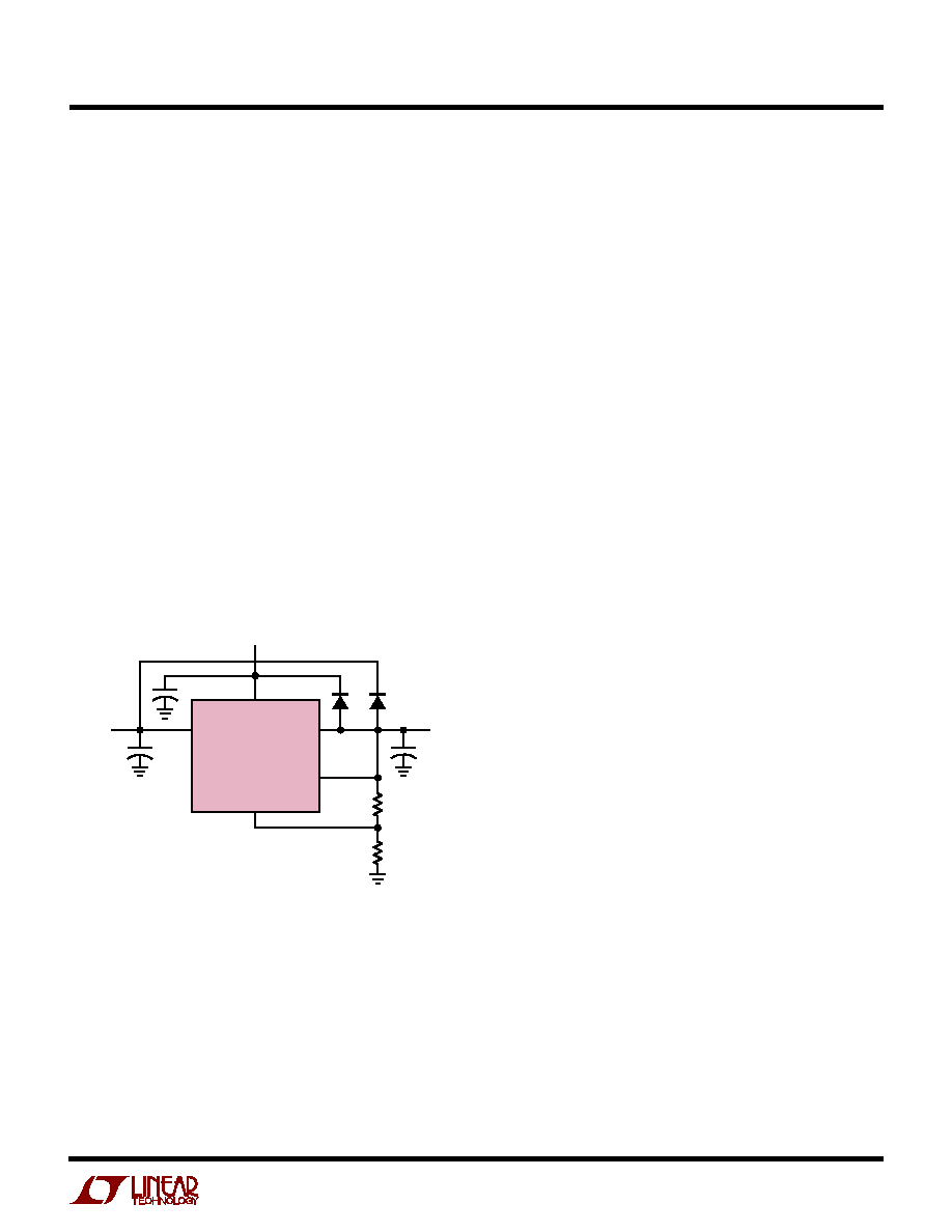
recommended. This is shown in Figure 6. Normal power
supply cycling or system "hot-plugging and unplugging"
will not do any damage.
A protection diode between the OUTPUT pin and the
V
CONTROL
pin is usually not needed. An internal diode
between the OUTPUT pin and the V
CONTROL
pin on the
LT1581 can handle microsecond surge currents of 1A to
10A. This can only occur if the V
CONTROL
pin is instanta-
neously shorted to ground with a crowbar circuit with
large value output capacitors. Since the V
CONTROL
pin is
usually a low current supply, this condition is unlikely. A
protection diode from the OUTPUT pin to the V
CONTROL
pin
is recommended if the V
CONTROL
pin can be instanta-
neously shorted to ground. This is shown in Figure 6.
Normal power supply cycling or system "hot-plugging
and unplugging" will not do any damage.
OUTPUT
SENSE
ADJ
R2
1581 F06
LT1581
POWER
V
POWER
V
CONTROL
CONTROL
R1
V
OUT
D1*
D2*
*OPTIONAL DIODES: 1N4002
+
+
+
Figure 6. Optional Clamp Diodes Protect Against
Input Crowbar Circuits
If the LT1581 is connected as a single supply device with
the control and power input pins shorted together, the
internal diode between the output and the power input pins
will protect the control input pin.
Like any other regulator exceeding the maximum input-to-
output differential can cause the internal transistors to
break down and none of the internal protection circuitry is
then functional.

10
LT1581/LT1581-2.5
APPLICATIO
N
S I
N
FOR
M
ATIO
N
W
U
U
U
where I
CONTROL
is equal to between I
OUT
/100 (typ) and
I
OUT
/58 (max).
I
CONTROL
is a function of output current. A curve of
I
CONTROL
vs I
OUT
can be found in the Typical Performance
Characteristics curves.
The power in the output transistor is equal to:
P
OUTPUT
= (V
POWER
V
OUT
)(I
OUT
)
The total power is equal to:
P
TOTAL
= P
DRIVE
+ P
OUTPUT
Junction-to-case thermal resistance is specified from the
IC junction to the bottom of the case directly below the die.
This is the lowest resistance path for heat flow. Proper
mounting is required to ensure the best possible thermal
flow from this area of the package to the heat sink. Thermal
compound at the case-to-heat sink interface is strongly
recommended. If the case of the device must be electroni-
cally isolated, a thermally conductive spacer can be used
as long as the added contribution to thermal resistance is
considered. Please consult Linear Technology's "Mount-
ing Considerations for Power Semiconductors,"
1990
Linear Applications Handbook, Volume 1, Pages RR3-1 to
RR3-20. Note that the case of the LT1581 is electrically
connected to the output.
The following example illustrates how to calculate
maximum junction temperature. Using an LT1581 and
assuming:
V
CONTROL
(max continuous) = 5.25V (5V + 5%),
V
POWER
(max continuous) = 3.465V (3.3V + 5%),
V
OUT
= 2.5V, Iout = 4A,
T
A
= 70
°
C,
HEATSINK
= 4
°
C/W,
CASE-HEATSINK
= 1
°
C/W (with thermal compound)
Power dissipation under these conditions is equal to:
Total Power Dissipation = P
DRIVE
+ P
OUTPUT
P
DRIVE
= (V
CONTROL
V
OUT
) (I
CONTROL
)
I
CONTROL
= I
OUT
/58 = 4A/58 = 69mA
P
DRIVE
= (5.25V 2.5V)(69mA) = 190mW
P
OUTPUT
= (V
POWER
V
OUT
)(I
OUT
)
= ( 3.465V 2.5V)(4A) = 3.9W
Total Power Dissipation = 4.09W
Junction temperature will be equal to:
T
J
= T
A
+ P
TOTAL
(
HEATSINK
+
CASE-HEATSINK
+
JC
)
For the Control section:
T
J
= 70
°
C + 4.09W(4
°
C/W + 1
°
C/W + 0.65
°
C/W) = 93
°
C
93
°
C < 125
°
C = T
JMAX
for Control Section
For the Power section:
T
J
= 70
°
C + 4.09W (4
°
C/W + 1
°
C/W + 2.5
°
C/W) = 101
°
C
101
°
C < 150
°
C = T
JMAX
for Power Section
In both cases the junction temperature is below the
maximum rating for the respective sections, ensuring
reliable operation.
11
LT1581/LT1581-2.5
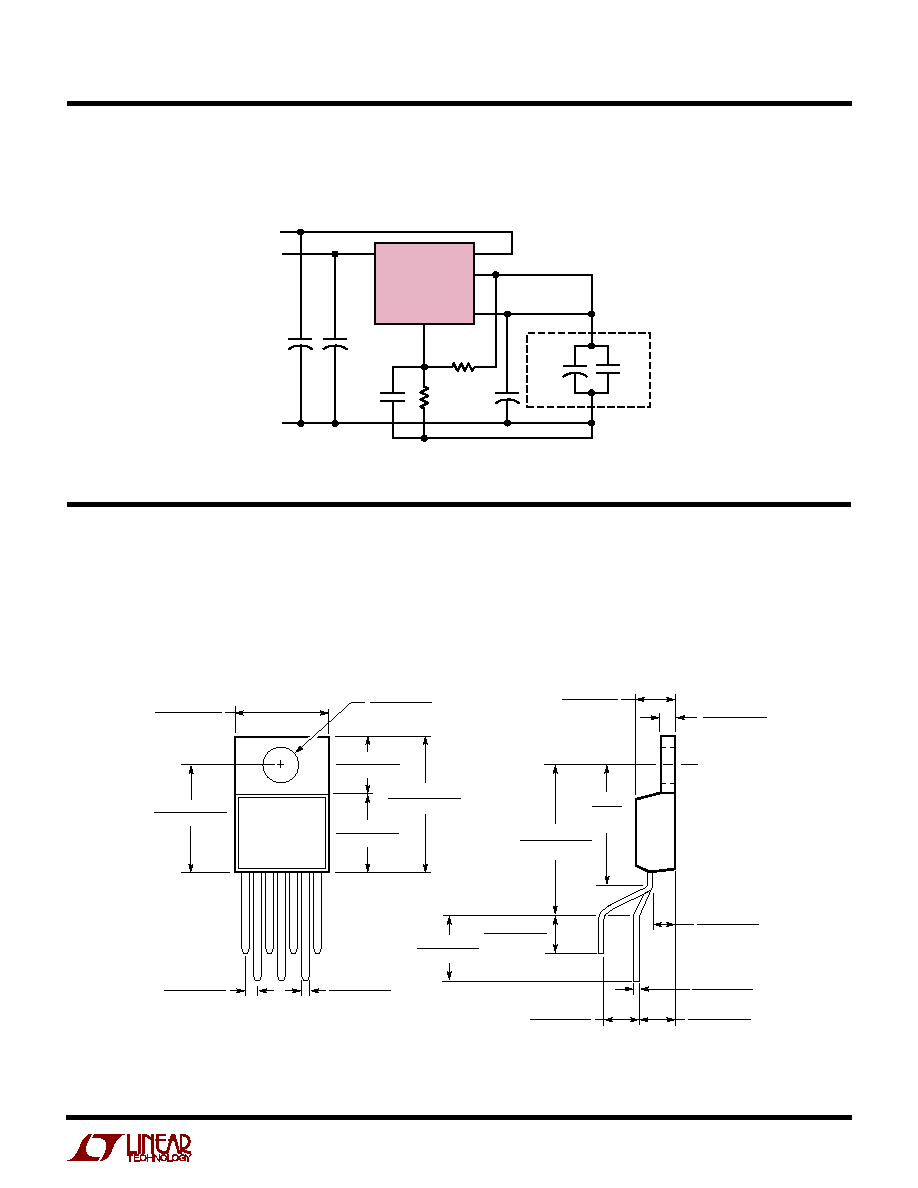
TYPICAL APPLICATIO
N
U
2.5V/10A Regulator
T7 Package
7-Lead Plastic TO-220 (Standard)
(LTC DWG # 05-08-1422)
PACKAGE DESCRIPTIO
N
U
Dimensions in inches (millimeters) unless otherwise noted.
Information furnished by Linear Technology Corporation is believed to be accurate and reliable.
However, no responsibility is assumed for its use. Linear Technology Corporation makes no represen-
tation that the interconnection of its circuits as described herein will not infringe on existing patent rights.
1581 TA03
+
+
+
C2
220
µ
F
10V
V
POWER
3
4
1
V
SS
6
V
CONT
5
3.3V
5V
RTN
SENSE
V
OUT
ADJ
R1
110
1%
V
OUT
= 2.5V
LT1581
C3
22
µ
F
25V
C4
0.33
µ
F
R2
110
1%
C1
100
µ
F
10V
+
V
CC
100
µ
F
10V
×
2
1
µ
F
25V
×
10
MICROPROCESSOR
SOCKET
0.040 0.060
(1.016 1.524)
0.026 0.036
(0.660 0.914)
T7 (TO-220) (FORMED) 1197
0.135 0.165
(3.429 4.191)
0.700 0.728
(17.780 18.491)
0.045 0.055
(1.143 1.397)
0.165 0.180
(4.191 4.572)
0.095 0.115
(2.413 2.921)
0.013 0.023
(0.330 0.584)
0.620
(15.75)
TYP
0.155 0.195
(3.937 4.953)
0.152 0.202
(3.860 5.130)
0.260 0.320
(6.604 8.128)
0.147 0.155
(3.734 3.937)
DIA
0.390 0.415
(9.906 10.541)
0.330 0.370
(8.382 9.398)
0.460 0.500
(11.684 12.700)
0.570 0.620
(14.478 15.748)
0.230 0.270
(5.842 6.858)
12
LT1581/LT1581-2.5
©
LINEAR TECHNOLOGY CORPORATION 1996
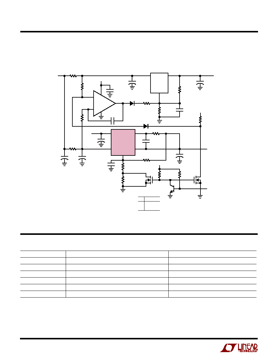
TYPICAL APPLICATIO
N
U
Dual Regulators Power Pentium Processor or Upgrade CPU
RELATED PARTS
PART NUMBER
DESCRIPTION
COMMENTS
LTC
®
1430
High Power Synchronous Step-Down Switching Regulator
> 90% Efficiency High Current Microprocessor Supply
LTC1435
High Current Synchronous Step-Down Controller
> 90% Efficiency in 12V to 3.3V Applications
LT1575/LT1577
Single and Dual Low Dropout Regulator Controllers
Fast Transient Response, No Bulk Capacitors Needed
LT1580
7A Fast Transient Response Regulator with 0.7V Dropout
For 3.3V to 2.XXV Applications
LT1584
7A Low Dropout Fast Transient Response Regulator
For High Performance Microprocessors
LT1585
4.6A Low Dropout Fast Transient Response Regulator
For High Performance Microprocessors
C1
220
µ
F
10V
C3
220
µ
F
10V
C10
1
µ
F
C9
220
µ
F
10V
C2
220
µ
F
10V
C5
0.33
µ
F
C11
22
µ
F
35V
LT1587
ADJ
V
IN
V
OUT
+
I/O
SUPPLY
3.5V/3.3V
C8
0.1
µ
F
C4
0.33
µ
F
C6
0.01
µ
F
R3
110
1%
R11
10k
R2
470
R14, 2
R13
0.005
*
R8
107
0.35%
R12
0.0075
*
D1
1N4148
D2
1N4148
R4
178
1%
R1
10k
5V
5V
12V
R10
10k
R7
107
0.25%
R5
10k
E3
TO CPU
VOLTAGE
SELECT PIN
5V
R9
10k
R6
89.8
0.5%
Q1
ZVN4206
Q2
2N3904
Q3
2N7002
1581 TA04
12V
3
4
1
CORE
SUPPLY
3.5V/2.5V
LT1006
C7
330
µ
F
6.3V
LT1581
6
5
V
CONT
V
POWER
SENSE
V
OUT
ADJ
*RESISTORS ARE IMPLEMENTED AS COPPER TRACES ON PCB
IF 1 OZ COPPER, TRACE WIDTHS ARE 0.05 INCH
IF 2 OZ COPPER, TRACE WIDTHS ARE 0.025 INCH
R13 IS 0.83 INCHES LONG, R12 IS 1.24 INCHES LONG
E3
0
1
CPU TYPE
P55C
P54C
+
+
+
+
+
+
Linear Technology Corporation
1630 McCarthy Blvd., Milpitas, CA 95035-7417
(408) 432-1900
q
FAX: (408) 434-0507
q
www.linear-tech.com
158125fa LT/TP 0399 2K REV A · PRINTED IN USA