 | ÐлекÑÑоннÑй компоненÑ: LT1614I | СкаÑаÑÑ:  PDF PDF  ZIP ZIP |
1614 Layout
1
LT1614
Inverting 600kHz
Switching Regulator
The LT
®
1614 is a fixed frequency, inverting mode switch-
ing reglator that operates from an input voltage as low as
1V. Utilizing a low noise topology, the LT1614 can gener-
ate a negative output down to 24V from a 1V to 5V input.
Fixed frequency switching ensures a clean output free
from low frequency noise. The device contains a low-
battery detector with a 200mV reference and shuts down
to less than 10
µ
A. No load quiescent current of the LT1614
is 1mA and the internal NPN power switch handles a
500mA current with a voltage drop of just 295mV.
High frequency switching enables the use of small induc-
tors and capacitors. Ceramic capacitors can be used in
many applications, eliminating the need for bulky tanta-
lum types.
The LT1614 is available in 8-lead MSOP or SO packages.
s
Better Regulation Than a Charge Pump
s
0.1
Effective Output Impedance
s
5V at 200mA from a 5V Input
s
600kHz Fixed Frequency Operation
s
Operates with V
IN
as Low as 1V
s
1mA Quiescent Current
s
Low Shutdown Current: 10
µ
A
s
Low-Battery Detector
s
Low V
CESAT
Switch: 295mV at 500mA
, LTC and LT are registered trademarks of Linear Technology Corporation.
s
MR Head Bias
s
LCD Bias
s
GaAs FET Bias
s
Positive-to-Negative Conversion
5V to 5V Converter Efficiency
Figure 1. 5V to 5V/200mA Converter
V
IN
SW
LT1614
L1
22
µ
H
V
IN
5V
D1
NFB
SHDN
69.8k
24.9k
100k
1nF
V
OUT
5V
200mA
C1, C2: AVX TAJB336M010
C3: TAIYO YUDEN EMK316BJ105MF
D1: MBR0520
L1, L2: MURATA LQH3C220
1614 TA01
C1
33
µ
F
C2
33
µ
F
V
C
GND
L2
22
µ
H
C3
1
µ
F
+
+
LOAD CURRENT (mA)
3
10
30
EFFICIENCY (%)
60
70
80
90
100
300
1614 TA02
50
40
APPLICATIO S
U
FEATURES
TYPICAL APPLICATIO
U
DESCRIPTIO
U
2
LT1614
A
U
G
W
A
W
U
W
A
R
BSOLUTE
XI
TI
S
V
IN
, SHDN, LBO Voltage ......................................... 12V
SW Voltage ............................................... 0.4V to 30V
NFB Voltage ............................................................ 3V
V
C
Voltage ................................................................ 2V
LBI Voltage ............................................ 0V
V
LBI
1V
Current into FB Pin ..............................................
±
1mA
Junction Temperature ........................................... 125
°
C
Operating Temperature Range
LT1614C ................................................. 0
°
C to 70
°
C
LT1614I ............................................. 40
°
C to 85
°
C
Extended Commercial
Temperature Range (Note 2) .................. 40
°
C to 85
°
C
Storage Temperature Range ................ 65
°
C to 150
°
C
Lead Temperature (Soldering, 10 sec)................. 300
°
C
ELECTRICAL C
C
HARA TERISTICS
PARAMETER
CONDITIONS
MIN
TYP
MAX
UNITS
Quiescent Current
1
2
mA
V
SHDN
= 0V
5
10
µ
A
Feedback Voltage
q
1.21
1.24
1.27
V
NFB Pin Bias Current (Note 3)
V
NFB
= 1.24V
q
2.5
4.5
7
µ
A
Reference Line Regulation
1V
V
IN
2V
0.6
1.1
%/V
2V
V
IN
6V
0.3
0.8
%/V
Minimum Input Voltage
0.92
1
V
Maximum Input Voltage
q
6
V
Error Amp Transconductance
I = 5
µ
A
16
µ
mhos
Error Amp Voltage Gain
100
V/V
Switching Frequency
q
500
600
750
kHz
Maximum Duty Cycle
73
80
%
q
70
80
%
Switch Current Limit (Note 4)
0.75
1.2
A
W
U
U
PACKAGE/ORDER I FOR ATIO
T
JMAX
= 125
°
C,
JA
= 160
°
C/W
Consult factory for Military grade parts.
ORDER PART
NUMBER
LT1614CS8
LT1614IS8
S8 PART MARKING
1614
1614I
ORDER PART
NUMBER
LT1614CMS8
LT1614IMS8
MS8 PART MARKING
LTID
LTJB
1
2
3
4
NFB
V
C
SHDN
GND
8
7
6
5
LBO
LBI
V
IN
SW
TOP VIEW
MS8 PACKAGE
8-LEAD PLASTIC MSOP
T
JMAX
= 125
°
C,
JA
= 120
°
C/W
1
2
3
4
8
7
6
5
TOP VIEW
LBO
LBI
V
IN
SW
NFB
V
C
SHDN
GND
S8 PACKAGE
8-LEAD PLASTIC SO
The
q
denotes the specifications which apply over the full operating
temperature range, otherwise specifications are at T
A
= 25
°
C. Commercial Grade 0
°
C to 70
°
C. V
IN
= 1.5V, V
SHDN
= V
IN
unless
otherwise noted.
(Note 1)
3
LT1614
PARAMETER
CONDITIONS
MIN
TYP
MAX
UNITS
Switch V
CESAT
I
SW
= 500mA (25
°
C, 0
°
C)
295
350
mV
I
SW
= 500mA (70
°
C)
400
mV
Shutdown Pin Current
V
SHDN
= V
IN
10
20
µ
A
V
SHDN
= 0V
5
10
µ
A
LBI Threshold Voltage
190
200
210
mV
q
185
215
mV
LBO Output Low
I
SINK
= 10
µ
A
0.1
0.25
V
LBO Leakage Current
V
LBI
= 250mV, V
LBO
= 5V
0.01
0.1
µ
A
LBI Input Bias Current (Note 5)
V
LBI
= 150mV
10
50
nA
Low-Battery Detector Gain
1M
Load
1000
V/V
Switch Leakage Current
V
SW
= 5V
0.01
3
µ
A
ELECTRICAL C
C
HARA TERISTICS
Note 1: Absolute Maximum Ratings are those values beyond which the life
of a device may be impaired.
Note 2: The LT1614C is guaranteed to meet specified performance from
0
°
C to 70
°
C and is designed, characterized and expected to meet these
extended temperature limits, but is not tested at 40
°
C and 85
°
C. The
LT1614I is guaranteed to meet the extended temperature limits.
Industrial Grade 40
°
C to 85
°
C. V
IN
= 1.5V, V
SHDN
= V
IN
unless otherwise noted.
PARAMETER
CONDITIONS
MIN
TYP
MAX
UNITS
Quiescent Current
1
2
mA
V
SHDN
= 0V
5
10
µ
A
Feedback Voltage
q
1.21
1.24
1.27
V
NFB Pin Bias Current (Note 3)
V
NFB
= 1.24V
q
2
4.5
7.5
µ
A
Reference Line Regulation
1V
V
IN
2V
0.6
1.1
%/V
2V
V
IN
6V
0.3
0.8
%/V
Minimum Input Voltage
40
°
C
1.1
1.25
V
85
°
C
0.8
1.0
V
Maximum Input Voltage
q
6
V
Error Amp Transconductance
I = 5
µ
A
16
µ
mhos
Error Amp Voltage Gain
100
V/V
Switching Frequency
q
500
600
750
kHz
Maximum Duty Cycle
q
70
80
%
Switch Current Limit (Note 4)
0.75
1.2
A
Switch V
CESAT
I
SW
= 500mA ( 40
°
C)
250
350
mV
I
SW
= 500mA (85
°
C)
330
400
mV
Shutdown Pin Current
V
SHDN
= V
IN
10
20
µ
A
V
SHDN
= 0V
5
10
µ
A
LBI Threshold Voltage
q
180
200
220
mV
LBO Output Low
I
SINK
= 10
µ
A
0.1
0.25
V
LBO Leakage Current
V
LBI
= 250mV, V
LBO
= 5V
0.1
0.3
µ
A
LBI Input Bias Current (Note 5)
V
LBI
= 150mV
5
30
nA
Low-Battery Detector Gain
1M
Load
1000
V/V
Switch Leakage Current
V
SW
= 5V
0.01
3
µ
A
Note 3: Bias current flows out of NFB pin.
Note 4: Switch current limit guaranteed by design and/or correlation to
static tests. Duty cycle affects current limit due to ramp generator.
Note 5: Bias current flows out of LBI pin.
The
q
denotes the specifications which apply over the full operating
temperature range, otherwise specifications are at T
A
= 25
°
C. Commercial Grade 0
°
C to 70
°
C. V
IN
= 1.5V, V
SHDN
= V
IN
unless
otherwise noted.
4
LT1614
TYPICAL PERFOR A CE CHARACTERISTICS
U
W
LBI Bias Current vs Temperature
Quiescent Current in Shutdown
Shutdown Pin Bias Current vs
Input Voltage
Switch V
CESAT
vs Current
Oscillator Frequency vs
Input Voltage
LBI Reference vs Temperature
TEMPERATURE (
°
C)
50
LBI BIAS CURRENT (nA)
25
75
1614 G03
25
0
50
16
14
12
10
8
6
4
2
0
100
SWITCH CURRENT (mA)
0
0
V
CESAT
(mV)
100
200
300
400
500
100
200
300
400
1614 G04
500
600
T
A
= 25
°
C
TEMPERATURE (
°
C)
50
REFERENCE VOLTAGE (mV)
25
0
25
50
1614 G05
75
210
208
206
204
202
200
198
196
194
192
190
100
INPUT VOLTAGE (V)
1
FREQUENCY (kHz)
600
700
5
1614 G06
500
400
2
3
4
900
800
85
°
C
40
°
C
25
°
C
INPUT VOLTAGE (V)
0
1
2
3
4
5
QUIESCENT CURRENT (
µ
A)
1614 G01
10
8
6
4
2
0
INPUT VOLTAGE (V)
0
1
2
3
4
5
SHDN BIAS CURRENT (
µ
A)
1614 G02
10
8
6
4
2
0
TEMPERATURE (
°
C)
50
0
50
25
25
75
100
V
NFB
(V)
1614 G09
1.245
1.240
1.235
1.230
1.225
1.220
1.215
1.210
V
NFB
vs Temperature
NFB Pin Bias Current vs
Temperature
TEMPERATURE (
°
C)
50
0
50
25
25
75
100
NFB PIN BIAS CURRENT (
µ
A)
1614 G08
6
5
4
3
2
1
0
TEMPERATURE (
°
C)
40
20
0
20
40
60
80
QUIESCENT CURRENT (mA)
1614 G07
6
5
4
3
2
1
0
V
IN
= 1.25V
V
IN
= 3V
V
IN
= 5V
Quiescent Current vs
Temperature*
*Includes diode leakage
5
LT1614
NFB (Pin 1): Negative Feedback Pin. Reference voltage is
1.24V. Connect resistive divider tap here. The sug-
gested value for R2 is 24.9k. Set R1 and R2 according to:
R
V
R
OUT
1
1 24
1 24
2
4 5 10
6
=
+
|
| .
.
. ·
V
C
(Pin 2): Compensation Pin for Error Amplifier. Con-
nect a series RC from this pin to ground. Typical values
are 100k
and 1nF. Minimize trace area at V
C
.
SHDN (Pin 3): Shutdown. Ground this pin to turn off
switcher. Must be tied to V
IN
(or higher voltage) to enable
switcher. Do not float the SHDN pin.
PI
N
FU
N
CTIO
N
S
U
U
U
GND (Pin 4): Ground. Connect directly to local ground
plane.
SW (Pin 5): Switch Pin. Minimize trace area at this pin to
keep EMI down.
V
IN
(Pin 6): Supply Pin. Must have 1
µ
F ceramic bypass
capacitor right at the pin, connected directly to ground.
LBI (Pin 7): Low-Battery Detector Input. 200mV refer-
ence. Voltage on LBI must stay between ground and
700mV. Float this pin if not used.
LBO (Pin 8): Low-Battery Detector Output. Open collec-
tor, can sink 10
µ
A. A 1M
pull-up is recommended. Float
this pin if not used. The low-battery detector is disabled
when SHDN is low. LBO is high-Z in this state.
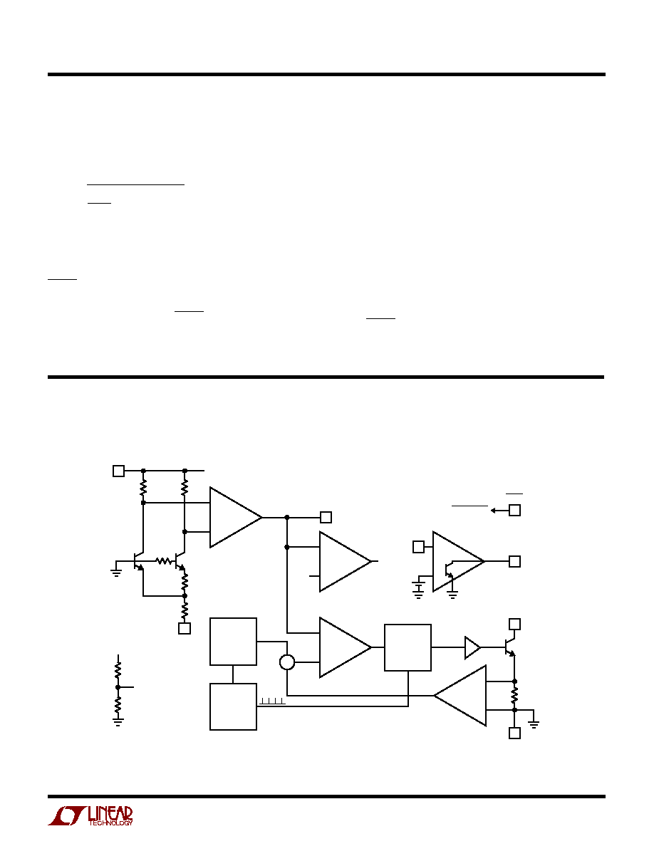
BLOCK DIAGRA
M
W
+
+
+
+
+
+
+
COMPARATOR
RAMP
GENERATOR
R
BIAS
V
C
g
m
Q2
×
10
Q1
NFB
NFB
ENABLE
200mV
A = 3
FF
A2
ERROR
AMPLIFIER
A1
A4
0.15
DRIVER
SW
GND
1614 BD
Q3
Q
S
600kHz
OSCILLATOR
5
LBO
LBI
SHDN
SHUTDOWN
3
7
2
4
R6
40k
R5
40k
R1
(EXTERNAL)
R3
30k
R4
140k
1
V
IN
V
IN
V
OUT
6
8
R2
(EXTERNAL)
Figure 2. Block Diagram