 | –≠–ª–µ–∫—Ç—Ä–æ–Ω–Ω—ã–π –∫–æ–º–ø–æ–Ω–µ–Ω—Ç: LT1615IS5 | –°–∫–∞—á–∞—Ç—å:  PDF PDF  ZIP ZIP |
1
LT1615/LT1615-1
Micropower Step-Up
DC/DC Converters
in ThinSOT
The LT
Æ
1615/LT1615-1 are micropower step-up DC/DC
converters in a 5-lead low profile (1mm) ThinSOT pack-
age. The LT1615 is designed for higher power systems
with a 350mA current limit and an input voltage range of
1.2V to 15V, whereas the LT1615-1 is intended for lower
power and single-cell applications with a 100mA current
limit and an extended input voltage range of 1V to 15V.
Otherwise, the two devices are functionally equivalent.
Both devices feature a quiescent current of only 20
µ
A at no
load, which further reduces to 0.5
µ
A in shutdown. A
current limited, fixed off-time control scheme conserves
operating current, resulting in high efficiency over a broad
range of load current. The 36V switch allows high voltage
outputs up to 34V to be easily generated in a simple boost
topology without the use of costly transformers. The
LT1615's low off-time of 400ns permits the use of tiny, low
profile inductors and capacitors to minimize footprint and
cost in space-conscious portable applications.
s
Low Quiescent Current:
20
µ
A in Active Mode
<1
µ
A in Shutdown Mode
s
Operates with V
IN
as Low as 1V
s
Low V
CESAT
Switch: 250mV at 300mA
s
Uses Small Surface Mount Components
s
High Output Voltage: Up to 34V
s
Low Profile (1mm) ThinSOT
TM
Package
s
LCD Bias
s
Handheld Computers
s
Battery Backup
s
Digital Cameras
, LTC and LT are registered trademarks of Linear Technology Corporation.
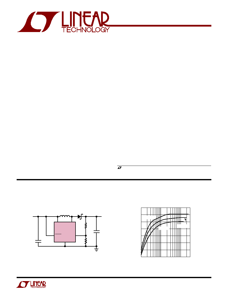
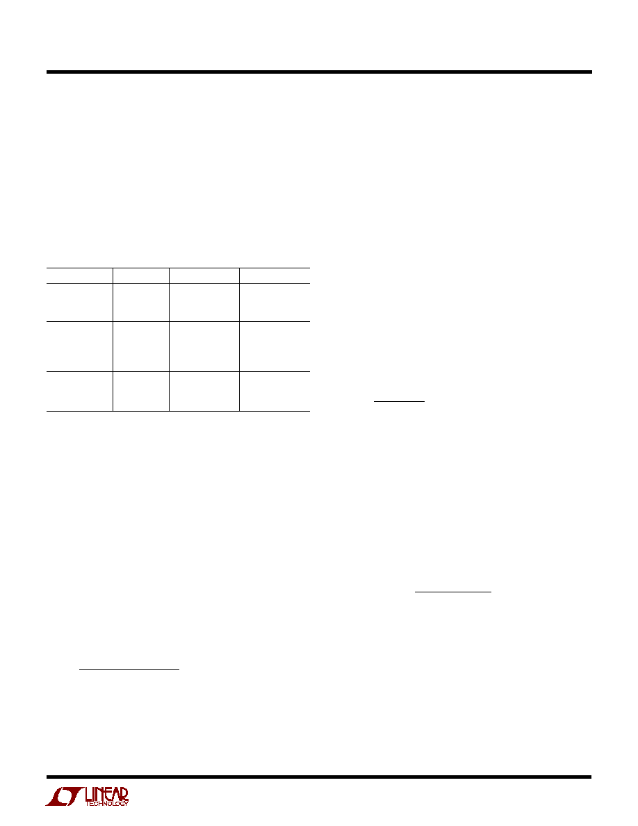
1-Cell Li-Ion to 20V Converter for LCD Bias
V
IN
SW
FB
LT1615
V
IN
2.5V TO 4.2V
L1
10
µ
H
D1
SHDN
R2
130k
R1
2M
C2
1
µ
F
20V
12mA
C1: TAIYO YUDEN LMK316BJ475
C2: TAIYO YUDEN TMK316BJ105
D1: MOTOROLA MBR0530
L1: MURATA LQH3C100K24
1615/-1 TA01
GND
C1
4.7
µ
F
Efficiency
LOAD CURRENT (mA)
0.1
0.3
EFFICIENCY (%)
1
3
10
30
1615
/-1
TA01a
85
80
75
70
65
60
55
50
V
IN
= 4.2V
V
IN
= 2.5V
V
IN
= 3.3V
APPLICATIO S
U
FEATURES
TYPICAL APPLICATIO
U
DESCRIPTIO
U
ThinSOT is a trademark of Linear Technology Corporation.
2
LT1615/LT1615-1
ABSOLUTE AXI U
RATI GS
W
W
W
U
PACKAGE/ORDER I FOR ATIO
U
U
W
(Note 1)
V
IN
, SHDN Voltage ................................................... 15V
SW Voltage .............................................................. 36V
FB Voltage .................................................................V
IN
Current into FB Pin ................................................. 1mA
Junction Temperature ........................................... 125
∞
C
Operating Temperature Range (Note 2) .. ≠ 40
∞
C to 85
∞
C
Storage Temperature Range ................. ≠ 65
∞
C to 150
∞
C
Lead Temperature (Soldering, 10 sec).................. 300
∞
C
ORDER PART
NUMBER
LT1615ES5
LT1615ES5-1
LT1615IS5
S5 PART MARKING
SW 1
GND 2
TOP VIEW
S5 PACKAGE
5-LEAD PLASTIC SOT-23
FB 3
5 V
IN
4 SHDN
ELECTRICAL CHARACTERISTICS
The
q
denotes the specifications which apply over the full operating
PARAMETER
CONDITIONS
MIN
TYP
MAX
UNITS
Minimum Input Voltage
LT1615-1
1.0
V
LT1615
1.2
V
Quiescent Current
Not Switching
20
30
µ
A
V
SHDN
= 0V
1
µ
A
FB Comparator Trip Point
q
1.205
1.23
1.255
V
FB Comparator Hysteresis
8
mV
Output Voltage Line Regulation
1.2V < V
IN
< 12V
0.05
0.1
%/V
FB Pin Bias Current (Note 3)
V
FB
= 1.23V
q
30
80
nA
Switch Off Time
V
FB
> 1V
400
ns
V
FB
< 0.6V
1.5
µ
s
Switch V
CESAT
I
SW
= 70mA (LT1615-1)
85
120
mV
I
SW
= 300mA (LT1615)
250
350
mV
Switch Current Limit
LT1615-1
75
100
125
mA
LT1615
300
350
400
mA
SHDN Pin Current
V
SHDN
= 1.2V
2
3
µ
A
V
SHDN
= 5V
8
12
µ
A
SHDN Input Voltage High
0.9
V
SHDN Input Voltage Low
0.25
V
Switch Leakage Current
Switch Off, V
SW
= 5V
0.01
5
µ
A
Note 1: Absolute Maximum Ratings are those values beyond which the life
of a device may be impaired.
Note 2: The LT1615E and LT1615E-1 are guaranteed to meet performance
specifications from 0
∞
C to 70
∞
C. Specifications over the
≠ 40
∞
C to 85
∞
C operating temperature range are assured by design,
T
JMAX
= 125
∞
C,
JA
= 256
∞
C/W
temperature range, otherwise specifications are at T
A
= 25
∞
C. V
IN
= 1.2V, V
SHDN
= 1.2V unless otherwise noted.
LTIZ
LTKH
LTXZ
Consult LTC Marketing for parts specified with wider operating temperature
ranges.
characterization and correlation with statistical process controls. The
LT1615I is guaranteed to meet performance specifications over the ≠40
∞
C
to 85
∞
C operating temperature range.
Note 3: Bias current flows into the FB pin.
3
LT1615/LT1615-1
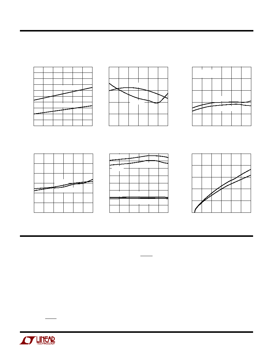
TYPICAL PERFOR A CE CHARACTERISTICS
U
W
Switch Saturation Voltage
(V
CESAT
)
Quiescent Current
Feedback Pin Voltage and
Bias Current
TEMPERATURE (
∞
C)
≠50
≠25
0
25
50
75
100
SWITCH VOLTAGE (V)
1615/-1 G01
0.60
0.55
0.50
0.45
0.40
0.35
0.30
0.25
0.20
0.15
0.10
I
SWITCH
= 500mA
I
SWITCH
= 300mA
TEMPERATURE (
∞
C)
≠50
FEEDBACK VOLTAGE (V)
1615/-1 G02
1.25
1.24
1.23
1.22
1.21
1.20
BIAS CURRENT (nA)
50
40
30
20
10
0
CURRENT
VOLTAGE
≠25
0
25
50
75
100
TEMPERATURE (
∞
C)
QUIESCENT CURRENT (
µ
A)
1615/-1 G03
25
23
21
19
17
15
≠50
≠25
0
25
50
75
100
V
IN
= 12V
V
IN
= 1.2V
V
FB
= 1.23V
NOT SWITCHING
PI FU CTIO S
U
U
U
SW (Pin 1): Switch Pin. This is the collector of the internal
NPN power switch. Minimize the metal trace area con-
nected to this pin to minimize EMI.
GND (Pin 2): Ground. Tie this pin directly to the local
ground plane.
FB (Pin 3): Feedback Pin. Set the output voltage by
selecting values for R1 and R2 (see Figure 1):
R
R
V
OUT
1
2
1 23
1
=
-
.
SHDN (Pin 4): Shutdown Pin. Tie this pin to 0.9V or higher
to enable the device. Tie below 0.25V to turn off the device.
V
IN
(Pin 5): Input Supply Pin. Bypass this pin with a
capacitor as close to the device as possible.
TEMPERATURE (
∞
C)
SWITCH OFF TIME (ns)
1615/-1 G04
550
500
450
400
350
300
250
≠50
≠25
0
25
50
75
100
V
IN
= 1.2V
V
IN
= 12V
TEMPERATURE (
∞
C)
PEAK CURRENT (mA)
1615/-1 G05
400
350
300
250
200
150
100
50
0
≠50
≠25
0
25
50
75
100
V
IN
= 12V
V
IN
= 1.2V
V
IN
= 12V
LT1615-1
LT1615
V
IN
= 1.2V
SHUTDOWN PIN VOLTAGE (V)
SHUTDOWN PIN CURRENT (
µ
A)
1615/-1 G03
25
20
15
10
5
0
0
5
10
15
25
∞
C
100
∞
C
Switch Off Time
Shutdown Pin Current
Switch Current Limit
4
LT1615/LT1615-1
BLOCK DIAGRA
W
Figure 1. LT1615 Block Diagram
≠
+
≠
+
5
400ns
ONE-SHOT
DRIVER
RESET
ENABLE
42mV*
0.12
A2
A1
Q3
2
R4
140k
R3
30k
R6
40k
R5
40k
Q2
X10
Q1
3
V
IN
FB
4
SHDN
1
SW
GND
1615/-1 BD
L1
C2
V
OUT
V
IN
D1
R2
(EXTERNAL)
R1
(EXTERNAL)
V
OUT
C1
* 12mV FOR LT1615-1
OPERATIO
U
The LT1615 uses a constant off-time control scheme to
provide high efficiencies over a wide range of output
current. Operation can be best understood by referring to
the block diagram in Figure 1. Q1 and Q2 along with R3 and
R4 form a bandgap reference used to regulate the output
voltage. When the voltage at the FB pin is slightly above
1.23V, comparator A1 disables most of the internal cir-
cuitry. Output current is then provided by capacitor C2,
which slowly discharges until the voltage at the FB pin
drops below the lower hysteresis point of A1 (typical
hysteresis at the FB pin is 8mV). A1 then enables the
internal circuitry, turns on power switch Q3, and the
current in inductor L1 begins ramping up. Once the switch
current reaches 350mA, comparator A2 resets the one-
shot, which turns off Q3 for 400ns. L1 then delivers
current to the output through diode D1 as the inductor
current ramps down. Q3 turns on again and the inductor
current ramps back up to 350mA, then A2 resets the one-
shot, again allowing L1 to deliver current to the output.
This switching action continues until the output voltage is
charged up (until the FB pin reaches 1.23V), then A1 turns
off the internal circuitry and the cycle repeats. The LT1615
contains additional circuitry to provide protection during
start-up and under short-circuit conditions. When the FB
pin voltage is less than approximately 600mV, the switch
off-time is increased to 1.5
µ
s and the current limit is
reduced to around 250mA (70% of its normal value). This
reduces the average inductor current and helps minimize
the power dissipation in the LT1615 power switch and in
the external inductor and diode. The LT1615-1 operates in
the same manner, except the switch current is limited to
100mA (the A2 reference voltage is 12mV instead of
42mV).
5
LT1615/LT1615-1
Choosing an Inductor
Several recommended inductors that work well with the
LT1615 and LT1615-1 are listed in Table 1, although there
are many other manufacturers and devices that can be
used. Consult each manufacturer for more detailed infor-
mation and for their entire selection of related parts. Many
different sizes and shapes are available. Use the equations
and recommendations in the next few sections to find the
correct inductance value for your design.
Table 1. Recommended Inductors
PART
VALUE (
µ
H)
MAX DCR (
)
VENDOR
LQH3C4R7
4.7
0.26
Murata
LQH3C100
10
0.30
(814) 237-1431
LQH3C220
22
0.92
www.murata.com
CD43-4R7
4.7
0.11
Sumida
CD43-100
10
0.18
(847) 956-0666
CDRH4D18-4R7
4.7
0.16
www.sumida.com
CDRH4D18-100
10
0.20
DO1608-472
4.7
0.09
Coilcraft
DO1608-103
10
0.16
(847) 639-6400
DO1608-223
22
0.37
www.coilcraft.com
Inductor Selection--Boost Regulator
The formula below calculates the appropriate inductor
value to be used for a boost regulator using the LT1615 or
LT1615-1 (or at least provides a good starting point). This
value provides a good tradeoff in inductor size and system
performance. Pick a standard inductor close to this value.
A larger value can be used to slightly increase the available
output current, but limit it to around twice the value
calculated below, as too large of an inductance will in-
crease the output voltage ripple without providing much
additional output current. A smaller value can be used
(especially for systems with output voltages greater than
12V) to give a smaller physical size. Inductance can be
calculated as:
L
V
V
V
I
t
OUT
IN MIN
D
LIM
OFF
=
-
+
( )
where V
D
= 0.4V (Schottky diode voltage), I
LIM
= 350mA or
100mA, and t
OFF
= 400ns; for designs with varying V
IN
such as battery powered applications, use the minimum
APPLICATIO S I FOR ATIO
W
U
U
U
V
IN
value in the above equation. For most systems with
output voltages below 7V, a 4.7
µ
H inductor is the best
choice, even though the equation above might specify a
smaller value. This is due to the inductor current over-
shoot that occurs when very small inductor values are
used (see Current Limit Overshoot section).
For higher output voltages, the formula above will give
large inductance values. For a 2V to 20V converter (typical
LCD Bias application), a 21
µ
H inductor is called for with
the above equation, but a 10
µ
H inductor could be used
without excessive reduction in maximum output current.
Inductor Selection--SEPIC Regulator
The formula below calculates the approximate inductor
value to be used for a SEPIC regulator using the LT1615.
As for the boost inductor selection, a larger or smaller
value can be used.
L
V
V
I
t
OUT
D
LIM
OFF
=
+
2
Current Limit Overshoot
For the constant off-time control scheme of the LT1615,
the power switch is turned off only after the 350mA (or
100mA) current limit is reached. There is a 100ns delay
between the time when the current limit is reached and
when the switch actually turns off. During this delay, the
inductor current exceeds the current limit by a small
amount. The peak inductor current can be calculated by:
I
I
V
V
L
ns
PEAK
LIM
IN MAX
SAT
=
+
-
(
)
100
Where V
SAT
= 0.25V (switch saturation voltage). The
current overshoot will be most evident for systems with
high input voltages and for systems where smaller induc-
tor values are used. This overshoot can be beneficial as it
helps increase the amount of available output current for
smaller inductor values. This will be the peak current seen
by the inductor (and the diode) during normal operation.
For designs using small inductance values (especially at
6
LT1615/LT1615-1
APPLICATIO S I FOR ATIO
W
U
U
U
input voltages greater than 5V), the current limit over-
shoot can be quite high. Although it is internally current
limited to 350mA, the power switch of the LT1615 can
handle larger currents without problem, but the overall
efficiency will suffer. Best results will be obtained when
I
PEAK
is kept below 700mA for the LT1615 and below
400mA for the LT1615-1.
Capacitor Selection
Low ESR (Equivalent Series Resistance) capacitors should
be used at the output to minimize the output ripple voltage.
Multilayer ceramic capacitors are the best choice, as they
have a very low ESR and are available in very small
packages. Their small size makes them a good companion
to the LT1615's SOT-23 package. Solid tantalum capaci-
tors (like the AVX TPS, Sprague 593D families) or OS-CON
capacitors can be used, but they will occupy more board
area than a ceramic and will have a higher ESR. Always use
a capacitor with a sufficient voltage rating.
Ceramic capacitors also make a good choice for the input
decoupling capacitor, which should be placed as close as
possible to the LT1615. A 4.7
µ
F input capacitor is suffi-
cient for most applications. Table 2 shows a list of several
capacitor manufacturers. Consult the manufacturers for
more detailed information and for their entire selection of
related parts.
Diode Selection
For most LT1615 applications, the Motorola MBR0520
surface mount Schottky diode (0.5A, 20V) is an ideal
choice. Schottky diodes, with their low forward voltage
drop and fast switching speed, are the best match for the
LT1615. For higher output voltage applications the 30V
MBR0530 can be used. Many different manufacturers
make equivalent parts, but make sure that the component
is rated to handle at least 0.35A. For LT1615-1 applica-
tions, a Philips BAT54 or Central Semiconductor CMDSH-3
works well.
Lowering Output Voltage Ripple
Using low ESR capacitors will help minimize the output
ripple voltage, but proper selection of the inductor and the
output capacitor also plays a big role. The LT1615 pro-
vides energy to the load in bursts by ramping up the
inductor current, then delivering that current to the load.
If too large of an inductor value or too small of a capacitor
value is used, the output ripple voltage will increase
because the capacitor will be slightly overcharged each
burst cycle. To reduce the output ripple, increase the
output capacitor value or add a 4.7pF feed-forward capaci-
tor in the feedback network of the LT1615 (see the circuits
in the Typical Applications section). Adding this small,
inexpensive 4.7pF capacitor will greatly reduce the output
voltage ripple.
Table 2. Recommended Capacitors
CAPACITOR TYPE
VENDOR
Ceramic
Taiyo Yuden
(408) 573-4150
www.t-yuden.com
Ceramic
AVX
(803) 448-9411
www.avxcorp.com
Ceramic
Murata
(714) 852-2001
www.murata.com
7
LT1615/LT1615-1
TYPICAL APPLICATIO S
U
2-Cell to 3.3V Boost Converter
V
IN
SW
FB
LT1615
V
IN
1.5V TO 3V
L1
4.7
µ
H
D1
SHDN
604k
1M
C2
22
µ
F
3.3V
60mA
1615/-1 TA03
GND
C1
4.7
µ
F
C1: TAIYO YUDEN LMK316BJ475
(408) 573-4150
C2: TAIYO YUDEN JMK325BJ226
(408) 573-4150
L1: MURATA LQH3C4R7M24
(814) 237-1431
D1: MOTOROLA MBR0520
(800) 441-2447
4
3
2
1
5
4.7pF
LOAD CURRENT (mA)
0.1
EFFICIENCY (%)
90
85
80
75
70
65
60
55
50
1
10
100
1615/-1 TA03a
V
IN
= 3V
V
IN
= 1.5V
2-Cell to 3.3V Converter Efficiency
1-Cell to 3.3V Boost Converter
4-Cell to 5V SEPIC Converter
V
IN
SW
FB
LT1615
V
IN
3V TO 6V
L1
10
µ
H
D1
C3
1
µ
F
SHDN
324k
1M
C2
10
µ
F
5V
40mA
1615/-1 TA07
GND
C1
4.7
µ
F
C1: TAIYO YUDEN LMK316BJ475
(408) 573-4150
C2: TAIYO YUDEN JMK316BJ106
(408) 573-4150
C3: TAIYO YUDEN JMK107BJ105
(408) 573-4150
L1, L2: MURATA LQH3C100K24
(814) 237-1431
D1: MOTOROLA MBR0520
(800) 441-2447
L2
10
µ
H
4
3
2
1
5
4.7pF
1-Cell Li-Ion to 3.3V SEPIC Converter
V
IN
SW
FB
LT1615
V
IN
2.5V TO 4.2V
L1
10
µ
H
D1
C3
1
µ
F
SHDN
604k
1M
C2
10
µ
F
3.3V
50mA
1615/-1 TA07
GND
C1
4.7
µ
F
C1: TAIYO YUDEN LMK316BJ475
(408) 573-4150
C2: TAIYO YUDEN JMK316BJ106
(408) 573-4150
C3: TAIYO YUDEN JMK107BJ105
(408) 573-4150
L1, L2: MURATA LQH3C100K24
(814) 237-1431
D1: MOTOROLA MBR0520
(800) 441-2447
L2
10
µ
H
4
3
2
1
5
4.7pF
Information furnished by Linear Technology Corporation is believed to be accurate and reliable.
However, no responsibility is assumed for its use. Linear Technology Corporation makes no represen-
tation that the interconnection of its circuits as described herein will not infringe on existing patent rights.
V
IN
SW
FB
LT1615-1
V
IN
1V TO 1.5V
L1
22
µ
H
D1
SHDN
604k
1M
C2
10
µ
F
3.3V
15mA
1615/-1 TA04
GND
C1
4.7
µ
F
C1: TAIYO YUDEN LMK316BJ475
(408) 573-4150
C2: TAIYO YUDEN JMK316BJ106
(408) 573-4150
L1: MURATA LQH3C220K24
(814) 237-1431
D1: CENTRAL SEMICONDUCTOR CMDSH-3
(516) 435-1110
4
3
2
1
5
4.7pF
PIN Diode Driver
V
IN
SW
FB
LT1615-1
V
IN
1V TO 6V
L1
22
µ
H
D1
SHDN
365k
10M
C2
1
µ
F
35V
500
µ
A
1615/-1 TA09
GND
C1
4.7
µ
F
C1: TAIYO YUDEN EMK316BJ475
(408) 573-4150
C2: TAIYO YUDEN GMK316BJ105
(408) 573-4150
L1: MURATA LQH3C220K24
(814) 237-1431
D1: MOTOROLA MBR0540
(800) 441-2447
4
3
2
1
5
8
LT1615/LT1615-1
Linear Technology Corporation
1630 McCarthy Blvd., Milpitas, CA 95035-7417
(408) 432-1900
q
FAX: (408) 434-0507
q
www.linear-tech.com
©
LINEAR TECHNOLOGY CORPORATION 1998
16151fa LT/TP 0601 1.5K REV A ∑ PRINTED IN USA
RELATED PARTS
PART NUMBER
DESCRIPTION
COMMENTS
LT1307
Single-Cell Micropower 600kHz PWM DC/DC Converter
3.3V at 75mA from One Cell, MSOP Package
LT1316
Burst Mode
TM
Operation DC/DC with Programmable Current Limit
1.5V Minimum, Precise Control of Peak Current Limit
LT1317
2-Cell Micropower DC/DC with Low-Battery Detector
3.3V at 200mA from Two Cells, 600kHz Fixed Frequency
LT1610
Single-Cell Micropower DC/DC Converter
3V at 30mA from 1V, 1.7MHz Fixed Frequency
LT1611
1.4MHz Inverting Switching Regulator in 5-Lead ThinSOT
≠ 5V at 150mA from 5V Input, Tiny ThinSOT Package
LT1613
1.4MHz Switching Regulator in 5-Lead ThinSOT
5V at 200mA from 3.3V Input, Tiny ThinSOT Package
LT1617
Micropower Inverting DC/DC Converter in 5-Lead ThinSOT
≠15V at 12mA from 2.5V Input, Tiny ThinSOT Package
Burst Mode is a trademark of Linear Technology Corporation
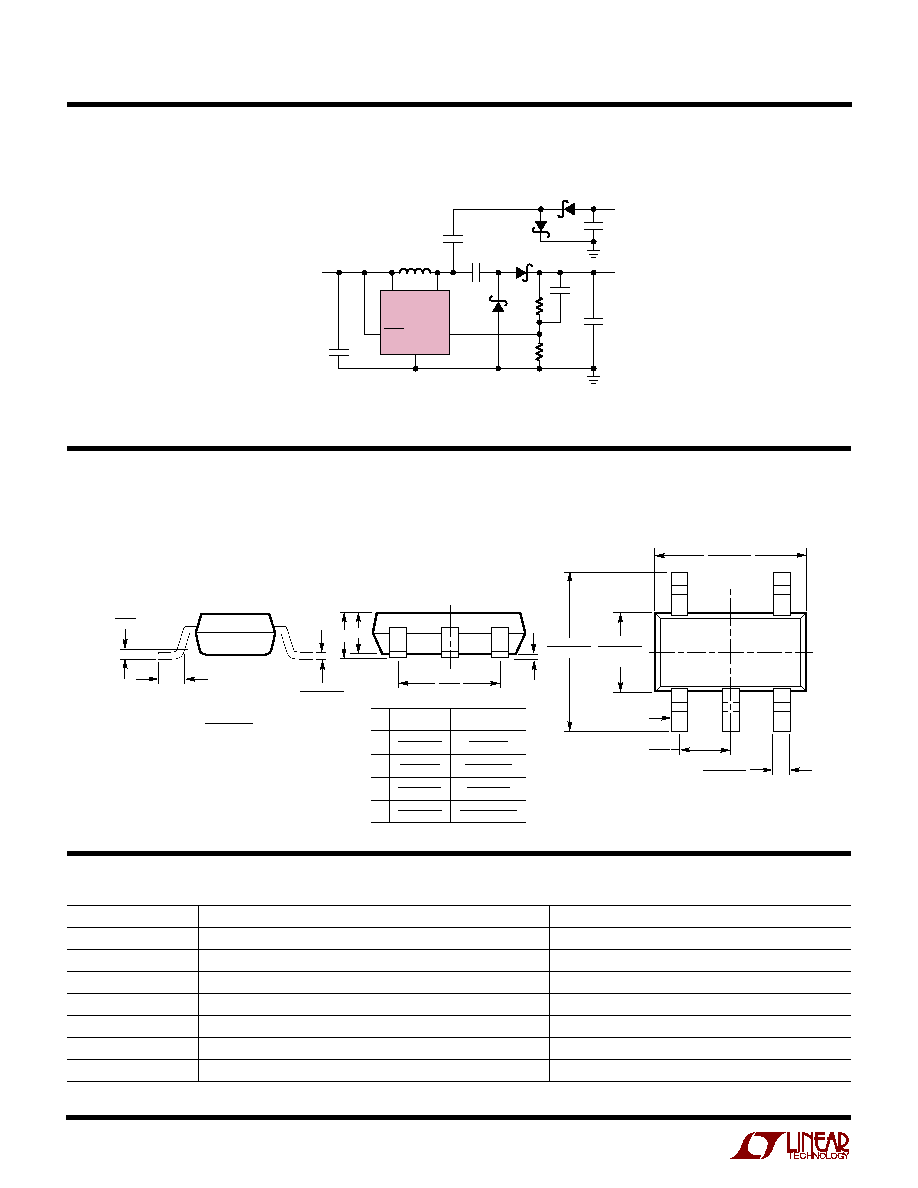
PACKAGE DESCRIPTIO
U
TYPICAL APPLICATIO S
U
V
IN
SW
FB
LT1615
V
IN
1.5V TO 5V
L1
10
µ
H
D1
D4
SHDN
130k
2M
C2
1
µ
F
20V
4mA
≠20V
4mA
1615/-1 TA05
GND
C3
1
µ
F
C1
4.7
µ
F
C1: TAIYO YUDEN LMK316BJ475
(408) 573-4150
C2, C3, C4: TAIYO YUDEN TMK316BJ105 (408) 573-4150
C5: TAIYO YUDEN LMK212BJ105
(408) 573-4150
L1: MURATA LQH3C100K24
(814) 237-1431
D1, D2, D3, D4: MOTOROLA MBR0530
(800) 441-2447
4
3
2
1
5
4.7pF
C4
1
µ
F
C5
1
µ
F
D3
D2
±
20V Dual Output Converter with Output Disconnect
S5 Package
5-Lead Plastic SOT-23
(Reference LTC DWG # 05-08-1633)
(Reference LTC DWG # 05-08-1635)
L
DATUM `A'
.09 ≠ .20
(.004 ≠ .008)
(NOTE 2)
A1
S5 SOT-23 0401
1.50 ≠ 1.75
(.059 ≠ .069)
(NOTE 3)
2.60 ≠ 3.00
(.102 ≠ .118)
.25 ≠ .50
(.010 ≠ .020)
(5PLCS, NOTE 2)
PIN ONE
2.80 ≠ 3.10
(.110 ≠ .118)
(NOTE 3)
.95
(.037)
REF
A A2
1.90
(.074)
REF
.20
(.008)
MILLIMETERS
(INCHES)
NOTE:
1. CONTROLLING DIMENSION: MILLIMETERS
2. DIMENSIONS ARE IN
3. DRAWING NOT TO SCALE
4. DIMENSIONS ARE INCLUSIVE OF PLATING
5. DIMENSIONS ARE EXCLUSIVE OF MOLD FLASH AND METAL BURR
6. MOLD FLASH SHALL NOT EXCEED .254mm
7. PACKAGE EIAJ REFERENCE IS:
SC-74A (EIAJ) FOR ORIGINAL
JEDEL MO-193 FOR THIN
.90 ≠ 1.45
(.035 ≠ .057)
SOT-23
(Original)
.00 ≠ .15
(.00 ≠ .006)
.90 ≠ 1.30
(.035 ≠ .051)
.35 ≠ .55
(.014 ≠ .021)
1.00 MAX
(.039 MAX)
SOT-23
(ThinSOT)
A
A1
A2
L
.01 ≠ .10
(.0004 ≠ .004)
.80 ≠ .90
(.031 ≠ .035)
.30 ≠ .50 REF
(.012 ≠ .019 REF)