 | ÐлекÑÑоннÑй компоненÑ: LT1636IS8 | СкаÑаÑÑ:  PDF PDF  ZIP ZIP |
Äîêóìåíòàöèÿ è îïèñàíèÿ www.docs.chipfind.ru
1
LT1636
Over-The-Top
Micropower Rail-to-Rail
Input and Output Op Amp
s
Rail-to-Rail Input and Output
s
Micropower: 50
µ
A I
Q
, 44V Supply
s
MSOP Package
s
Over-The-Top
TM
: Input Common Mode Range
Extends 44V Above V
EE
, Independent of V
CC
s
Low Input Offset Voltage: 225
µ
V Max
s
Specified on 3V, 5V and
±
15V Supplies
s
High Output Current: 18mA
s
Output Shutdown
s
Output Drives 10,000pF with Output Compensation
s
Reverse Battery Protection to 27V
s
High Voltage Gain: 2000V/mV
s
High CMRR: 110dB
s
220kHz Gain-Bandwidth Product
The LT
®
1636 op amp operates on all single and split supplies
with a total voltage of 2.7V to 44V drawing less than 50
µ
A of
quiescent current. The LT1636 can be shut down, making the
output high impedance and reducing the quiescent current to
4
µ
A. The LT1636 has a unique input stage that operates and
remains high impedance when above the positive supply. The
inputs take 44V both differential and common mode, even
when operating on a 3V supply. The output swings to both
supplies. Unlike most micropower op amps, the LT1636 can
drive heavy loads; its rail-to-rail output drives 18mA. The
LT1636 is unity-gain stable into all capacitive loads up to
10,000pF when a 0.22
µ
F and 150
compensation network
is used.
The LT1636 is reverse supply protected: it draws no current
for reverse supply up to 27V. Built-in resistors protect the
inputs for faults below the negative supply up to 22V. There
is no phase reversal of the output for inputs 5V below V
EE
or
44V above V
EE
, independent of V
CC
.
The LT1636 op amp is available in the 8-pin MSOP, PDIP and
SO packages.
, LTC and LT are registered trademarks of Linear Technology Corporation.
Over-The-Top is a trademark of Linear Technology Corporation.
COMMON MODE VOLTAGE (V)
4.0
10
INPUT BIAS CURRENT (nA)
0
20
30
40
5.2 10 20 30 40
5000
1636 G03
10
4.4
4.8
50
1000
3000
V
S
= 5V, 0V
T
A
= 55
°
C
T
A
= 125
°
C
T
A
= 25
°
C
Input Bias Current vs Common Mode Voltage
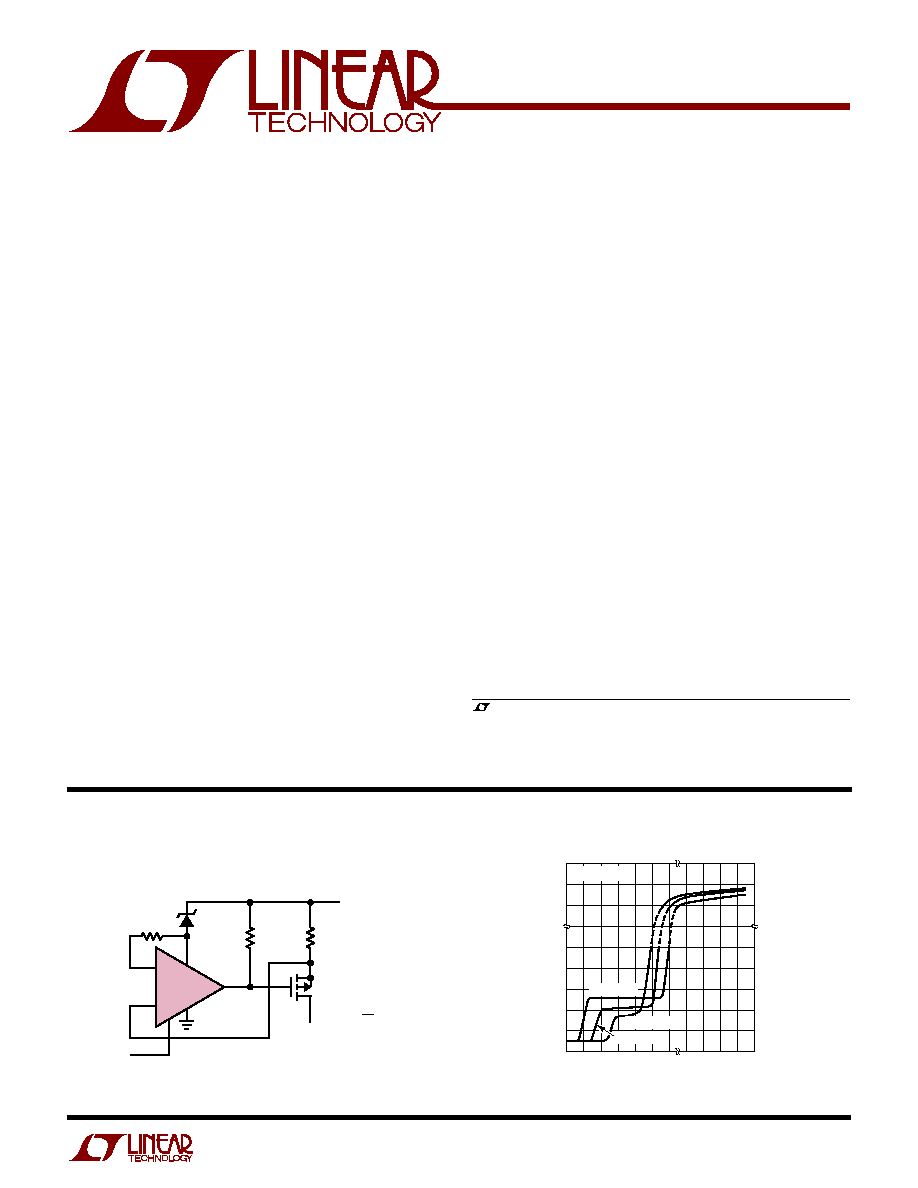
Over-The-Top Current Source with Shutdown
SHDN
I
OUT
LT1004-1.2
1M
*OPTIONAL FOR LOW OUTPUT CURRENTS
4V TO
44V
R
J176
1636 TA01
R*
+
LT1636
I
OUT
=
e.g., 10mA = 120
1.2
R
s
Battery- or Solar-Powered Systems
Portable Instrumentation
Sensor Conditioning
s
Supply Current Sensing
s
Battery Monitoring
s
MUX Amplifiers
s
4mA to 20mA Transmitters
FEATURES
DESCRIPTIO
U
APPLICATIO S
U
TYPICAL APPLICATIO
U
2
LT1636
ABSOLUTE
M
AXI
M
U
M
RATINGS
W
W
W
U
Total Supply Voltage (V
+
to V
) .............................. 44V
Input Differential Voltage ......................................... 44V
Input Current ......................................................
±
25mA
Shutdown Pin Voltage Above V
............................. 32V
Shutdown Pin Current .......................................
±
10mA
Output Short-Circuit Duration (Note 2) ......... Continuous
Operating Temperature Range ................ 40
°
C to 85
°
C
Specified Temperature Range (Note 3) .. 40
°
C to 85
°
C
Junction Temperature ........................................... 150
°
C
Storage Temperature Range ................. 65
°
C to 150
°
C
Lead Temperature (Soldering, 10 sec).................. 300
°
C
V
S
= 3V, 0V; V
S
= 5V, 0V; V
CM
= V
OUT
= half supply, Pin 5 = open or
V
EE
, Pins 1 and 8 open, T
A
= 25
°
C unless otherwise noted. (Note 3)
3V, 5V ELECTRICAL CHARACTERISTICS
SYMBOL
PARAMETER
CONDITIONS
MIN
TYP
MAX
UNITS
V
OS
Input Offset Voltage
N8 Package
50
225
µ
V
0
°
C
T
A
70
°
C
q
400
µ
V
40
°
C
T
A
85
°
C
q
550
µ
V
S8 Package
50
225
µ
V
0
°
C
T
A
70
°
C
q
600
µ
V
40
°
C
T
A
85
°
C
q
750
µ
V
MS8 Package
50
225
µ
V
0
°
C
T
A
70
°
C
q
700
µ
V
40
°
C
T
A
85
°
C
q
850
µ
V
Input Offset Voltage Drift (Note 8)
N8 Package, 40
°
C
T
A
85
°
C
q
1
5
µ
V/
°
C
S8 Package, 40
°
C
T
A
85
°
C
q
2
8
µ
V/
°
C
MS8 Package, 40
°
C
T
A
85
°
C
q
2
10
µ
V/
°
C
I
OS
Input Offset Current
q
0.1
0.8
nA
V
CM
= 44V (Note 4)
q
0.6
µ
A
I
B
Input Bias Current
q
5
8
nA
V
CM
= 44V (Note 4)
q
3
6
µ
A
V
S
= 0V
0.1
nA
Input Noise Voltage
0.1Hz to 10Hz
0.7
µ
V
P-P
e
n
Input Noise Voltage Density
f = 1kHz
52
nV/
Hz
i
n
Input Noise Current Density
f = 1kHz
0.035
pA/
Hz
PACKAGE/ORDER I
N
FOR
M
ATIO
N
W
U
U
MS8 PART MARKING
S8 PART MARKING
Consult factory for Military grade parts.
1636
1636I
LT1636CN8
LT1636CS8
LT1636IN8
LT1636IS8
LT1636CMS8
LTCL
ORDER PART
NUMBER
ORDER PART
NUMBER
T
JMAX
= 150
°
C,
JA
= 130
°
C/ W (N8)
T
JMAX
= 150
°
C,
JA
= 190
°
C/ W (S8)
1
2
3
4
8
7
6
5
TOP VIEW
NULL
IN
+IN
V
NULL
V
+
OUT
SHDN
N8 PACKAGE
8-LEAD PLASTIC DIP
S8 PACKAGE
8-LEAD PLASTIC SO
1
2
3
4
8
7
6
5
TOP VIEW
MS8 PACKAGE
8-LEAD PLASTIC MSOP
NULL
IN
+IN
V
NULL
V
+
OUT
SHDN
T
JMAX
= 150
°
C,
JA
= 250
°
C/ W
(Note 1)
3
LT1636
3V, 5V ELECTRICAL CHARACTERISTICS
SYMBOL
PARAMETER
CONDITIONS
MIN
TYP
MAX
UNITS
R
IN
Input Resistance
Differential
6
10
M
Common Mode, V
CM
= 0V to 44V
7
15
M
C
IN
Input Capacitance
4
pF
Input Voltage Range
q
0
44
V
CMRR
Common Mode Rejection Ratio
V
CM
= 0V to V
CC
1V
q
84
110
dB
(Note 4)
V
CM
= 0V to 44V (Note 7)
q
86
98
dB
A
VOL
Large-Signal Voltage Gain
V
S
= 3V, V
O
= 500mV to 2.5V, R
L
= 10k
200
1300
V/mV
V
S
= 3V, 0
°
C
T
A
70
°
C
q
133
V/mV
V
S
= 3V, 40
°
C
T
A
85
°
C
q
100
V/mV
V
S
= 5V, V
O
= 500mV to 4.5V, R
L
= 10k
400
2000
V/mV
V
S
= 5V, 0
°
C
T
A
70
°
C
q
250
V/mV
V
S
= 5V, 40
°
C
T
A
85
°
C
q
200
V/mV
V
OL
Output Voltage Swing LOW
No Load
q
2
10
mV
I
SINK
= 5mA
q
480
875
mV
V
S
= 5V, I
SINK
= 10mA
q
860
1600
mV
V
OH
Output Voltage Swing HIGH
V
S
= 3V, No Load
q
2.95
2.985
V
V
S
= 3V, I
SOURCE
= 5mA
q
2.55
2.8
V
V
S
= 5V, No Load
q
4.95
4.985
V
V
S
= 5V, I
SOURCE
= 10mA
q
4.30
4.75
V
I
SC
Short-Circuit Current (Note 2)
V
S
= 3V, Short to GND
7
15
mA
V
S
= 3V, Short to V
CC
20
42
mA
V
S
= 5V, Short to GND
12
25
mA
V
S
= 5V, Short to V
CC
25
50
mA
PSRR
Power Supply Rejection Ratio
V
S
= 2.7V to 12.5V, V
CM
= V
O
= 1V
q
90
103
dB
Reverse Supply Voltage
I
S
= 100
µ
A
q
27
40
V
I
S
Supply Current (Note 5)
42
55
µ
A
q
60
µ
A
Supply Current, SHDN
V
PIN5
= 2V, No Load (Note 5)
q
4
12
µ
A
I
SD
Shutdown Pin Current
V
PIN5
= 0.3V, No Load (Note 5)
q
0.5
15
nA
V
PIN5
= 2V, No Load (Note 4)
q
1.1
5
µ
A
Output Leakage Current
V
PIN5
= 2V, No Load (Note 5)
q
0.05
1
µ
A
Maximum Shutdown Pin Current
V
PIN5
= 32V, No Load (Note 4)
q
27
150
µ
A
t
ON
Turn-On Time
V
PIN5
= 5V to 0V, R
L
= 10k
120
µ
s
t
OFF
Turn-Off Time
V
PIN5
= 0V to 5V, R
L
= 10k
2.5
µ
s
GBW
Gain Bandwidth Product
f = 1kHz
110
200
kHz
(Note 4)
0
°
C
T
A
70
°
C
q
100
kHz
40
°
C
T
A
85
°
C
q
90
kHz
SR
Slew Rate
A
V
= 1, R
L
=
0.035
0.07
V/
µ
s
(Note 6)
0
°
C
T
A
70
°
C
q
0.031
V/
µ
s
40
°
C
T
A
85
°
C
q
0.030
V/
µ
s
V
S
= 3V, 0V; V
S
= 5V, 0V; V
CM
= V
OUT
= half supply, Pin 5 = open or
V
EE
, Pins 1 and 8 open, T
A
= 25
°
C unless otherwise noted. (Note 3)
4
LT1636
SYMBOL
PARAMETER
CONDITIONS
MIN
TYP
MAX
UNITS
V
OS
Input Offset Voltage
N8 Package
100
450
µ
V
0
°
C
T
A
70
°
C
q
550
µ
V
40
°
C
T
A
85
°
C
q
700
µ
V
S8 Package
100
450
µ
V
0
°
C
T
A
70
°
C
q
750
µ
V
40
°
C
T
A
85
°
C
q
900
µ
V
MS8 Package
100
450
µ
V
0
°
C
T
A
70
°
C
q
850
µ
V
40
°
C
T
A
85
°
C
q
1000
µ
V
Input Offset Voltage Drift (Note 8)
N8 Package, 40
°
C
T
A
85
°
C
q
1
4
µ
V/
°
C
S8 Package, 40
°
C
T
A
85
°
C
q
2
8
µ
V/
°
C
MS8 Package, 40
°
C
T
A
85
°
C
q
2
10
µ
V/
°
C
I
OS
Input Offset Current
q
0.2
1.0
nA
I
B
Input Bias Current
q
4
10
nA
Input Noise Voltage
0.1Hz to 10Hz
1
µ
V
P-P
e
n
Input Noise Voltage Density
f = 1kHz
52
nV/
Hz
i
n
Input Noise Current Density
f = 1kHz
0.035
pA/
Hz
R
IN
Input Resistance
Differential
5.2
13
M
Common Mode, V
CM
= 15V to 14V
12000
M
C
IN
Input Capacitance
4
pF
Input Voltage Range
q
15
29
V
CMRR
Common Mode Rejection Ratio
V
CM
= 15V to 29V
q
86
103
dB
A
VOL
Large-Signal Voltage Gain
V
O
=
±
14V, R
L
= 10k
100
500
V/mV
0
°
C
T
A
70
°
C
q
75
V/mV
40
°
C
T
A
85
°
C
q
50
V/mV
V
OL
Output Voltage Swing LOW
No Load
q
14.997
14.95
V
I
SINK
= 5mA
q
14.500
14.07
V
I
SINK
= 10mA
q
14.125
13.35
V
V
OH
Output Voltage Swing HIGH
No Load
q
14.9
14.975
V
I
SOURCE
= 5mA
q
14.5
14.750
V
I
SOURCE
= 10mA
q
14.3
14.650
V
I
SC
Short-Circuit Current (Note 2)
Short to GND
±
18
±
30
mA
0
°
C
T
A
70
°
C
q
±
15
mA
40
°
C
T
A
85
°
C
q
±
10
mA
PSRR
Power Supply Rejection Ratio
V
S
=
±
1.35V to
±
22V
q
90
114
dB
I
S
Supply Current
50
70
µ
A
q
85
µ
A
Positive Supply Current, SHDN
V
PIN5
= 20V, V
S
=
±
22V, No Load
q
12
30
µ
A
I
SHDN
Shutdown Pin Current
V
PIN5
= 21.7V, V
S
=
±
22V, No Load
q
0.7
15
nA
V
PIN5
= 20V, V
S
=
±
22V, No Load
q
1.2
8
µ
A
Maximum Shutdown Pin Current
V
PIN5
= 32V, V
S
=
±
22V
q
27
150
µ
A
Output Leakage Current
V
PIN5
= 20V, V
S
=
±
22V, No Load
q
0.1
2
µ
A
GBW
Gain Bandwidth Product
f = 1kHz
125
220
kHz
0
°
C
T
A
70
°
C
q
110
kHz
40
°
C
T
A
85
°
C
q
100
kHz
±
15V
ELECTRICAL CHARACTERISTICS
V
S
=
±
15V, V
CM
= 0V, V
OUT
= 0V, Pin 5 = open or
V
EE
, Pins 1 and 8 open, T
A
= 25
°
C unless otherwise noted. (Note 3)
5
LT1636
SYMBOL
PARAMETER
CONDITIONS
MIN
TYP
MAX
UNITS
SR
Slew Rate
A
V
= 1, R
L
=
, V
O
=
±
10V Measured at
±
5V
0.0375
0.075
V/
µ
s
0
°
C
T
A
70
°
C
q
0.033
V/
µ
s
40
°
C
T
A
85
°
C
q
0.030
V/
µ
s
V
S
=
±
15V, V
CM
= 0V, V
OUT
= 0V, Pin 5 = open or
V
EE
, Pins 1 and 8 open, T
A
= 25
°
C unless otherwise noted. (Note 3)
±
15V ELECTRICAL CHARACTERISTICS
Note 4: V
S
= 5V limits are guaranteed by correlation to V
S
= 3V, and
V
S
=
±
15V or V
S
=
±
22V tests.
Note 5: V
S
= 3V limits are guaranteed by correlation to V
S
= 5V, and
V
S
=
±
15V or V
S
=
±
22V tests.
Note 6: Guaranteed by correlation to slew rate at V
S
=
±
15V, and GBW at
V
S
= 3V and V
S
=
±
15V tests.
Note 7: This specification implies a typical input offset voltage of 600
µ
V at
V
CM
= 44V and a maximum input offset voltage of 3mV at V
CM
= 44V.
Note 8: This parameter is not 100% tested.
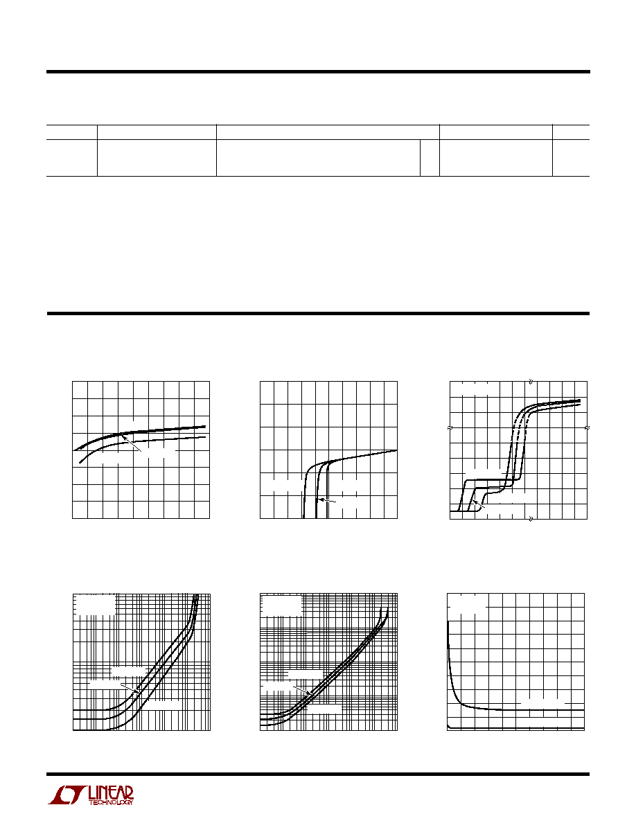
TYPICAL PERFOR A CE CHARACTERISTICS
U
W
TOTAL SUPPLY VOLTAGE (V)
0
SUPPLY CURRENT (
µ
A)
40
50
60
40
35
25
15
5
45
1636 G01
30
20
0
10
20
30
10
80
70
T
A
= 125
°
C
T
A
= 25
°
C
T
A
= 55
°
C
Supply Current vs Supply Voltage
COMMON MODE VOLTAGE (V)
4.0
10
INPUT BIAS CURRENT (nA)
0
20
30
40
5.2 10 20 30 40
5000
1636 G03
10
4.4
4.8
50
1000
3000
V
S
= 5V, 0V
T
A
= 55
°
C
T
A
= 125
°
C
T
A
= 25
°
C
Input Bias Current
vs Common Mode Voltage
SOURCING LOAD CURRENT (mA)
0.0001 0.001
0.01
OUTPUT SATURATION VOLTAGE (V)
0.1
1
0.01
0.1
1
10
100
1636 G04
V
S
= 5V
V
OD
= 30mV
T
A
= 125
°
C
T
A
= 25
°
C
T
A
= 55
°
C
Output Saturation Voltage
vs Load Current (Output High)
INPUT OVERDRIVE (mV)
0
OUTPUT SATURATION VOLTAGE (mV)
60
80
100
80
1636 G06
40
20
50
70
90
30
10
0
20
40
60
10
90
30
50
70
100
OUTPUT HIGH
OUTPUT LOW
V
S
=
±
2.5V
NO LOAD
Output Saturation Voltage
vs Input Overdrive
Output Saturation Voltage
vs Load Current (Output Low)
SINKING LOAD CURRENT (mA)
0.0001 0.001
0.001
0.01
OUTPUT SATURATION VOLTAGE (V)
0.1
1
10
0.01
0.1
1
10
100
1636 G05
V
S
= 5V
V
OD
= 30mV
T
A
= 125
°
C
T
A
= 55
°
C
T
A
= 25
°
C
Minimum Supply Voltage
TOTAL SUPPLY VOLTAGE (V)
CHANGE IN INPUT OFFSET VOLTAGE (
µ
V)
300
100
300
200
200
100
0
1
2
3
4
1636 G02
5
0
T
A
= 55
°
C
T
A
= 125
°
C
T
A
= 25
°
C
The
q
denotes specifications that apply over the full specified temperature
range.
Note 1: Absolute Maximum Ratings are those values beyond which the life
of a device may be impaired.
Note 2: A heat sink may be required to keep the junction temperature
below absolute maximum.
Note 3: The LT1636C is guaranteed to meet specified performance from
0
°
C to 70
°
C and is designed, characterized and expected to meet these
extended temperature limits, but is not tested at 40
°
C and 85
°
C. The
LT1636I is guaranteed to meet the extended temperature limits.