 | ÐлекÑÑоннÑй компоненÑ: LT1637 | СкаÑаÑÑ:  PDF PDF  ZIP ZIP |
Äîêóìåíòàöèÿ è îïèñàíèÿ www.docs.chipfind.ru
1
LT1637
The LT
®
1637 is a rugged op amp that operates on all single
and split supplies with a total voltage of 2.7V to 44V. The
LT1637 has a gain-bandwidth product of 1.1MHz while
drawing less than 250
µ
A of quiescent current. The LT1637
can be shut down, making the output high impedance and
reducing the quiescent current to only 3
µ
A. The LT1637 is
reverse supply protected: it draws virtually no current for
reverse supply up to 25V. The input range of the LT1637
includes both supplies and the output swings to both
supplies. Unlike most micropower op amps, the LT1637
can drive heavy loads; its rail-to-rail output drives 25mA.
The LT1637 is unity-gain stable into all capacitive loads up
to 4700pF when optional 0.22
µ
F and 150
compensation
is used.
The LT1637 has a unique input stage that operates and
remains high impedance when above the positive supply.
The inputs take 44V both differential and common mode,
even when operating on a 3V supply. Built-in resistors
protect the inputs for faults below the negative supply up
to 22V. There is no phase reversal of the output for inputs
5V below V
EE
or 44V above V
EE
, independent of V
CC
.
The LT1637 op amp is available in the 8-pin MSOP, PDIP
and SO packages.
s
Battery or Solar Powered Systems:
Portable Instrumentation
Sensor Conditioning
s
Supply Current Sensing
s
Battery Monitoring
s
MUX Amplifiers
s
4mA to 25mA Transmitters
, LTC and LT are registered trademarks of Linear Technology Corporation.
s
Operates with Inputs Above V
+
s
Rail-to-Rail Input and Output
s
Micropower: 250
µ
A Supply Current Max
s
Gain-Bandwidth Product: 1.1MHz
s
Slew Rate: 0.4V/
µ
s
s
Low Input Offset Voltage: 350
µ
V Max
s
Single Supply Input Range: 0.4V to 44V
s
High Output Current: 25mA Min
s
Specified on 3V, 5V and
±
15V Supplies
s
Output Shutdown
s
Output Drives 4700pF with Output Compensation
s
Reverse Battery Protection to 25V
s
High Voltage Gain: 800V/mV
s
High CMRR: 110dB
Over-The-Top is a trademark of Linear Technology Corporation.
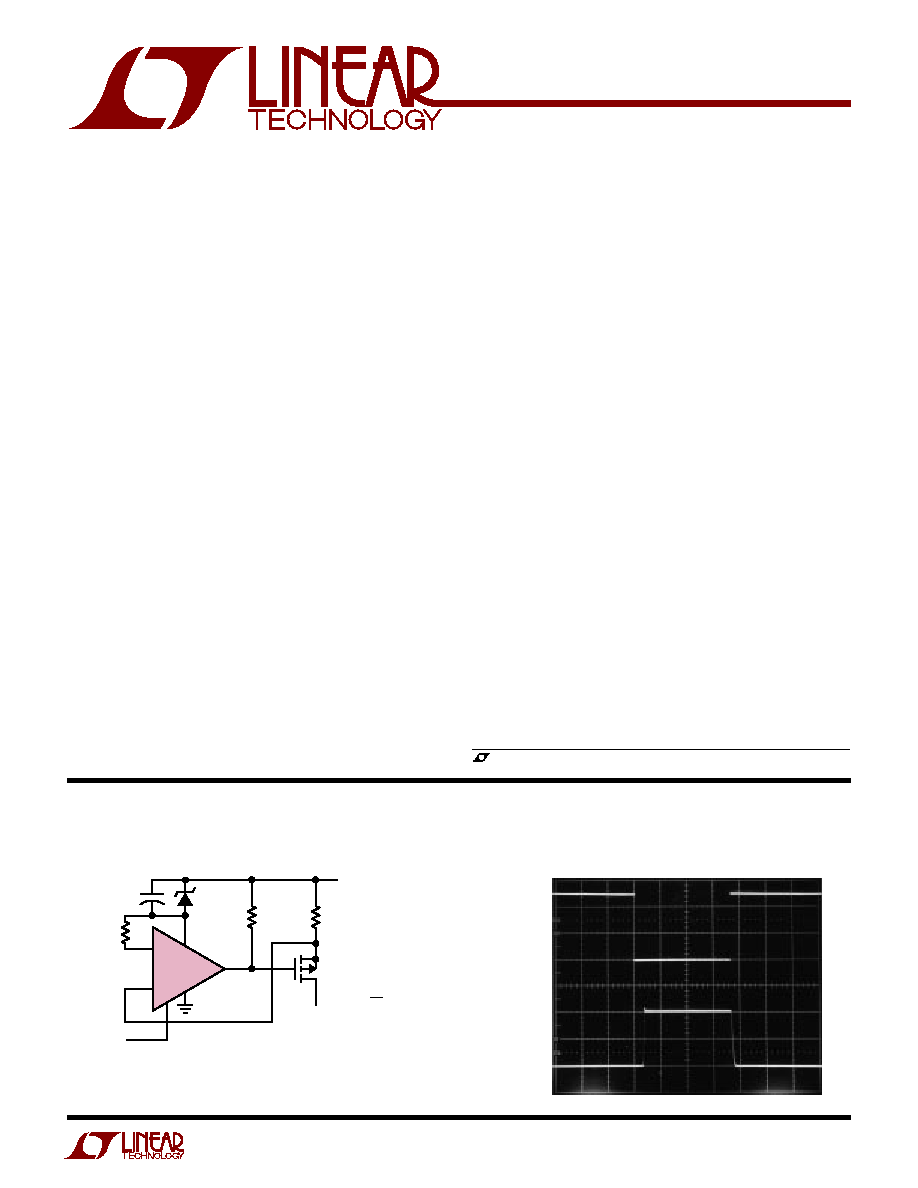
Over-The-Top
TM
Current Source with Shutdown
SHDN
I
OUT
LT1004-1.2
4.7
µ
F
2k
*OPTIONAL FOR LOW OUTPUT CURRENTS,
R* = R
R
4V TO 44V
TP0610
1637 TA01
R*
+
LT1637
I
OUT
=
e.g., 10mA = 120
1.2
R
+
V
SHDN
6V
4V
2V
0V
10mA
5mA
0mA
I
OUT
100
µ
s/DIV
1637 TA01b
Switchable Precision Current Source
Current Source Timing
APPLICATIO S
U
TYPICAL APPLICATIO
U
1.1MHz, 0.4V/
µ
s
Over-The-Top Micropower, Rail-To-Rail
Input and Output Op Amp
FEATURES
DESCRIPTIO
U
2
LT1637
Total Supply Voltage (V
+
to V
) .............................. 44V
Input Differential Voltage ......................................... 44V
Input Current ......................................................
±
25mA
Shutdown Pin Voltage Above V
.....................................
32V
Shutdown Pin Current ........................................
±
10mA
Output Short-Circuit Duration (Note 2) ......... Continuous
Consult factory for Military grade parts.
(Note 1)
ORDER PART
NUMBER
S8 PART
MARKING
1637
1637I
LT1637CN8
LT1637CS8
LT1637IN8
LT1637IS8
1
2
3
4
8
7
6
5
TOP VIEW
NULL
V
+
OUT
SHDN
NULL
IN
+
IN
V
S8 PACKAGE
8-LEAD PLASTIC SO
N8 PACKAGE
8-LEAD PDIP
T
JMAX
= 150
°
C,
JA
= 130
°
C/W (N8)
T
JMAX
= 150
°
C,
JA
= 190
°
C/W (S8)
SYMBOL
PARAMETER
CONDITIONS
MIN
TYP
MAX
UNITS
V
OS
Input Offset Voltage
N8, S8 Packages
100
350
µ
V
0
°
C
T
A
70
°
C
q
550
µ
V
40
°
C
T
A
85
°
C
q
700
µ
V
MS8 Package
100
350
µ
V
0
°
C
T
A
70
°
C
q
750
µ
V
40
°
C
T
A
85
°
C
q
900
µ
V
Input Offset Voltage Drift (Note 9)
N8, S8 Packages, 40
°
C
T
A
85
°
C
q
1
3
µ
V/
°
C
MS8 Package, 40
°
C
T
A
85
°
C
q
2
6
µ
V/
°
C
I
OS
Input Offset Current
q
0.4
6.0
nA
V
CM
= 44V (Note 5)
q
2.5
µ
A
I
B
Input Bias Current
q
20
50
nA
V
CM
= 44V (Note 5)
q
23
60
µ
A
V
S
= 0V
0.1
nA
Input Noise Voltage
0.1Hz to 10Hz
0.6
µ
V
P-P
e
n
Input Noise Voltage Density
f = 1kHz
27
nV/
Hz
i
n
Input Noise Current Density
f = 1kHz
0.08
pA/
Hz
The
q
denotes the specifications which apply over the specified temperature range, otherwise specifications are at T
A
= 25
°
C.
V
S
= 3V, 0V; V
S
= 5V, 0V; V
SHDN
= V
,V
CM
= V
OUT
= Half Supply unless otherwise specified. (Note 4)
3V
5V
A
U
D
ELECTRICAL CHARACTERISTICS
PACKAGE/ORDER I FOR ATIO
U
U
W
ABSOLUTE AXI U
RATI GS
W
W
W
U
Operating Temperature Range (Note 3) .. 40
°
C to 85
°
C
Specified Temperature Range (Note 4) ... 40
°
C to 85
°
C
Junction Temperature ........................................... 150
°
C
Storage Temperature Range ................. 65
°
C to 150
°
C
Lead Temperature (Soldering, 10 sec).................. 300
°
C
1
2
3
4
NULL
IN
+
IN
V
8
7
6
5
NULL
V
+
OUT
SHDN
TOP VIEW
MS8 PACKAGE
8-LEAD PLASTIC MSOP
ORDER PART
NUMBER
MS8 PART
MARKING
LTIE
LT1637CMS8
T
JMAX
= 150
°
C,
JA
= 250
°
C/W
3
LT1637
R
IN
Input Resistance
Differential
1
2.6
M
Common Mode, V
CM
= 0V to 44V
0.7
1.4
M
C
IN
Input Capacitance
4
pF
Input Voltage Range
q
0
44
V
CMRR
Common Mode Rejection Ratio
V
CM
= 0V to (V
CC
1V)
q
88
110
dB
(Note 5)
V
CM
= 0V to 44V (Note 8)
q
80
98
dB
A
VOL
Large-Signal Voltage Gain
V
S
= 3V, V
O
= 500mV to 2.5V, R
L
= 10k
150
400
V/mV
V
S
= 3V, 0
°
C
T
A
70
°
C
q
100
V/mV
V
S
= 3V, 40
°
C
T
A
85
°
C
q
75
V/mV
V
S
= 5V, V
O
= 500mV to 4.5V, R
L
= 10k
300
800
V/mV
V
S
= 5V, 0
°
C
T
A
70
°
C
q
200
V/mV
V
S
= 5V, 40
°
C
T
A
85
°
C
q
150
V/mV
V
OL
Output Voltage Swing LOW
No Load
q
3
8
mV
I
SINK
= 5mA
q
325
700
mV
V
S
= 5V, I
SINK
= 10mA
q
580
1300
mV
V
OH
Output Voltage Swing HIGH
V
S
= 3V, No Load
q
2.94
2.975
V
V
S
= 3V, I
SOURCE
= 5mA
q
2.25
2.67
V
V
S
= 5V, No Load
q
4.94
4.975
V
V
S
= 5V, I
SOURCE
= 10mA
q
3.80
4.45
V
I
SC
Short-Circuit Current (Note 2)
V
S
= 3V, Short Output to Ground
10
14
mA
V
S
= 3V, Short Output to V
CC
15
45
mA
V
S
= 5V, Short Output to Ground
15
22
mA
V
S
= 5V, Short Output to V
CC
15
60
mA
PSRR
Power Supply Rejection Ratio
V
S
= 3V to 12.5V, V
CM
= V
O
= 1V
q
90
98
dB
Minimum Supply Voltage
q
2.7
V
Reverse Supply Voltage
I
S
= 100
µ
A
q
25
40
V
I
S
Supply Current
190
250
µ
A
(Note 6)
q
295
µ
A
Supply Current, SHDN
V
PIN5
= 2V, No Load (Note 6)
q
3
12
µ
A
I
SHDN
Shutdown Pin Current
V
PIN5
= 0.3V, No Load (Note 6)
q
0.2
15
nA
V
PIN5
= 2V, No Load (Note 5)
q
1.0
5
µ
A
V
PIN5
= 3.3V
2.5
µ
A
V
PIN5
= 5V
4.3
µ
A
Output Leakage Current
V
PIN5
= 2V, No Load (Note 6)
q
0.02
1
µ
A
Maximum Shutdown Pin Current
V
PIN5
= 32V, No Load (Note 5)
q
20
150
µ
A
t
ON
Turn-On Time
V
PIN5
= 5V to 0V, R
L
= 10k
45
µ
s
t
OFF
Turn-Off Time
V
PIN5
= 0V to 5V, R
L
= 10k
3
µ
s
t
SETTLING
Settling Time
0.1% A
V
= 1,
V
O
= 2V
9
µ
s
GBW
Gain-Bandwidth Product
f = 10kHz
650
1000
kHz
(Note 5)
0
°
C
T
A
70
°
C
q
550
kHz
40
°
C
T
A
85
°
C
q
500
kHz
SR
Slew Rate
A
V
= 1, R
L
=
0.210
0.35
V/
µ
s
(Note 7)
0
°
C
T
A
70
°
C
q
0.185
V/
µ
s
40
°
C
T
A
85
°
C
q
0.170
V/
µ
s
SYMBOL
PARAMETER
CONDITIONS
MIN
TYP
MAX
UNITS
The
q
denotes the specifications which apply over the specified temperature range, otherwise specifications are at T
A
= 25
°
C.
V
S
= 3V, 0V; V
S
= 5V, 0V; V
SHDN
= V
, V
CM
= V
OUT
= Half Supply unless otherwise specified. (Note 4)
3V
5V
A
U
D
ELECTRICAL CHARACTERISTICS
4
LT1637
SYMBOL
PARAMETER
CONDITIONS
MIN
TYP
MAX
UNITS
V
OS
Input Offset Voltage
N8, S8 Packages
100
450
µ
V
0
°
C
T
A
70
°
C
q
650
µ
V
40
°
C
T
A
85
°
C
q
800
µ
V
MS8 Package
100
450
µ
V
0
°
C
T
A
70
°
C
q
800
µ
V
40
°
C
T
A
85
°
C
q
950
µ
V
Input Offset Voltage Drift (Note 9)
N8, S8 Packages, 40
°
C
T
A
85
°
C
q
1
3
µ
V/
°
C
MS8 Package, 40
°
C
T
A
85
°
C
q
2
6
µ
V/
°
C
I
OS
Input Offset Current
q
1
6
nA
I
B
Input Bias Current
q
17
50
nA
Input Noise Voltage
0.1Hz to 10Hz
0.6
µ
V
P-P
e
n
Input Noise Voltage Density
f = 1kHz
27
nV/
Hz
i
n
Input Noise Current Density
f = 1kHz
0.08
pA/
Hz
R
IN
Input Resistance
Differential
1
3
M
Common Mode, V
CM
= 15V to 14V
2200
M
C
IN
Input Capacitance
4
pF
Input Voltage Range
q
15
29
V
CMRR
Common Mode Rejection Ratio
V
CM
= 15V to 29V
q
80
110
dB
A
VOL
Large-Signal Voltage Gain
V
O
=
±
14V, R
L
= 10k
100
400
V/mV
0
°
C
T
A
70
°
C
q
75
V/mV
40
°
C
T
A
85
°
C
q
50
V/mV
V
OL
Output Voltage Swing LOW
No Load
q
14.997
14.95
V
I
SINK
= 5mA
q
14.680
14.25
V
I
SINK
= 10mA
q
14.420
13.65
V
V
OH
Output Voltage Swing HIGH
No Load
q
14.9
14.967
V
I
SOURCE
= 5mA
q
14.2
14.667
V
I
SOURCE
= 10mA
q
13.7
14.440
V
I
SC
Short-Circuit Current (Note 2)
Short Output to GND
±
25
±
31.7
mA
0
°
C
T
A
70
°
C
q
±
20
mA
40
°
C
T
A
85
°
C
q
±
15
mA
PSRR
Power Supply Rejection Ratio
V
S
=
±
1.5V to
±
22V
q
90
115
dB
Minimum Supply Voltage
q
±
1.35
V
I
S
Supply Current
230
300
µ
A
q
370
µ
A
Positive Supply Current, SHDN
V
PIN5
= 20V, V
S
=
±
22V, No Load
q
6
40
µ
A
I
SHDN
Shutdown Pin Current
V
PIN5
= 21.7V, V
S
=
±
22V, No Load
q
0.3
15
nA
V
PIN5
= 20V, V
S
=
±
22V, No Load
q
0.9
8
µ
A
Maximum Shutdown Pin Current
V
PIN5
= 32V, V
S
=
±
22V
q
20
150
µ
A
Output Leakage Current
V
PIN5
= 20V, V
S
=
±
22V, No Load
q
0.02
2
µ
A
V
L
Shutdown Pin Input Low Voltage
V
S
=
±
22V
q
21.7
21.6
V
V
H
Shutdown Pin Input High Voltage
V
S
=
±
22V
q
20.8
20.0
V
t
ON
Turn-On Time
V
PIN5
= 10V to 15V, R
L
= 10k
35
µ
s
t
OFF
Turn-Off Time
V
PIN5
= 15V to 10V, R
L
= 10k
3
µ
s
The
q
denotes the specifications which apply over the specified temperature range, otherwise specifications are at T
A
= 25
°
C.
V
S
=
±
15V, V
CM
= 0V, V
OUT
= 0V, V
SHDN
= V
unless otherwise specified. (Note 4)
±
15V ELECTRICAL CHARACTERISTICS
5
LT1637
GBW
Gain-Bandwidth Product
f = 10kHz
750
1100
kHz
0
°
C
T
A
70
°
C
q
650
kHz
40
°
C
T
A
85
°
C
q
600
kHz
SR
Slew Rate
A
V
= 1, R
L
=
, V
O
=
±
10V, Measure at V
O
=
±
5V
0.225
0.4
V/
µ
s
0
°
C
T
A
70
°
C
q
0.200
V/
µ
s
40
°
C
T
A
85
°
C
q
0.180
V/
µ
s
The
q
denotes the specifications which apply over the specified temperature range, otherwise specifications are at T
A
= 25
°
C.
V
S
=
±
15V, V
CM
= 0V, V
OUT
= 0V, V
SHDN
= V
unless otherwise specified. (Note 4)
SYMBOL
PARAMETER
CONDITIONS
MIN
TYP
MAX
UNITS
±
15V ELECTRICAL CHARACTERISTICS
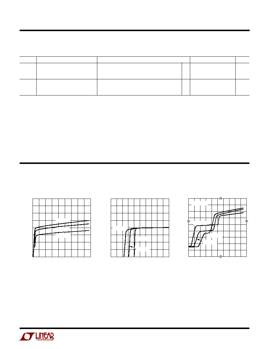
Supply Current vs Supply Voltage
Input Bias Current
vs Common Mode Voltage
Minimum Supply Voltage
TYPICAL PERFOR A CE CHARACTERISTICS
U
W
TOTAL SUPPLY VOLTAGE (V)
0
10
20
30
40
SUPPLY CURRENT (
µ
A)
1637 G01
400
350
300
250
200
150
100
50
0
T
A
= 125
°
C
T
A
= 25
°
C
T
A
= 55
°
C
TOTAL SUPPLY VOLTAGE (V)
0
1
2
3
4
5
CHANGE IN INPUT OFFSET VOLTAGE (
µ
V)
1637 G02
400
300
200
100
0
100
200
300
400
T
A
= 125
°
C
T
A
= 55
°
C
T
A
= 25
°
C
COMMON MODE VOLTAGE (V)
4
4.2 4.4 4.6 4.8
5
10 20 30 40 50
INPUT BIAS CURRENT (
µ
A)
40
30
20
10
0.12
0.08
0.04
0
0.04
0.08
1637 G03
V
S
= 5V, 0V
T
A
= 125
°
C
T
A
= 55
°
C
T
A
= 25
°
C
Note 1: Absolute Maximum Ratings are those values beyond which the life
of a device may be impaired.
Note 2: A heat sink may be required to keep the junction temperature
below absolute maximum.
Note 3: The LT1637 is guaranteed functional over the operating
temperature range of 40
°
C to 85
°
C.
Note 4: The LT1637C is guaranteed to meet specified performance from
0
°
C to 70
°
C. The LT1637C is designed, characterized and expected to
meet specified performance from 40
°
C to 85
°
C but is not tested or QA
sampled at these temperatures. The LT1637I is guaranteed to meet
specified performance from 40
°
C to 85
°
C.
Note 5: V
S
= 5V limits are guaranteed by correlation to V
S
= 3V and
V
S
=
±
15V or V
S
=
±
22V tests.
Note 6: V
S
= 3V limits are guaranteed by correlation to V
S
= 5V and
V
S
=
±
15V or V
S
=
±
22V tests.
Note 7: Guaranteed by correlation to slew rate at V
S
=
±
15V and GBW at
V
S
= 3V and V
S
=
±
15V tests.
Note 8: This specification implies a typical input offset voltage of 650
µ
V at
V
CM
= 44V and a maximum input offset voltage of 5.4mV at V
CM
= 44V.
Note 9: This parameter is not 100% tested.