ƒÓÍÛÏÂÌÚýˆËˇ Ë ÓÔËÒýÌˡ www.docs.chipfind.ru
1
LT1640L/LT1640H
Negative Voltage
Hot Swap Controller
FEATURES
s
Allows Safe Board Insertion and Removal
from a Live ≠ 48V Backplane
s
Operates from ≠10V to ≠ 80V
s
Programmable Inrush Current
s
Programmable Electronic Circuit Breaker
s
Programmable Overvoltage Protection
s
Programmable Undervoltage Lockout
s
Power Good Control Output
The LT
Æ
1640L/LT1640H is an 8-pin, negative voltage Hot
Swap
TM
controller that allows a board to be safely inserted
and removed from a live backplane. Inrush current is
limited to a programmable value by controlling the gate
voltage of an external N-channel pass transistor. The pass
transistor is turned off if the input voltage is less than the
programmable undervoltage threshold or greater than the
overvoltage threshold. A programmable electronic circuit
breaker protects the system against shorts. The PWRGD
(LTC1640L) or PWRGD (LTC1640H) signal can be used to
directly enable a power module. The LT1640L is designed
for modules with a low enable input and the LT1640H for
modules with a high enable input.
The LT1640L/LT1640H is available in 8-pin PDIP and SO
packages.
DESCRIPTIO
N
U
s
Central Office Switching
s
≠ 48V Distributed Power Systems
s
Negative Power Supply Control
APPLICATIO
N
S
U
Hot Swap is a trademark of Linear Technology Corporation.
, LTC and LT are registered trademarks of Linear Technology Corporation.
TYPICAL APPLICATIO
N
U
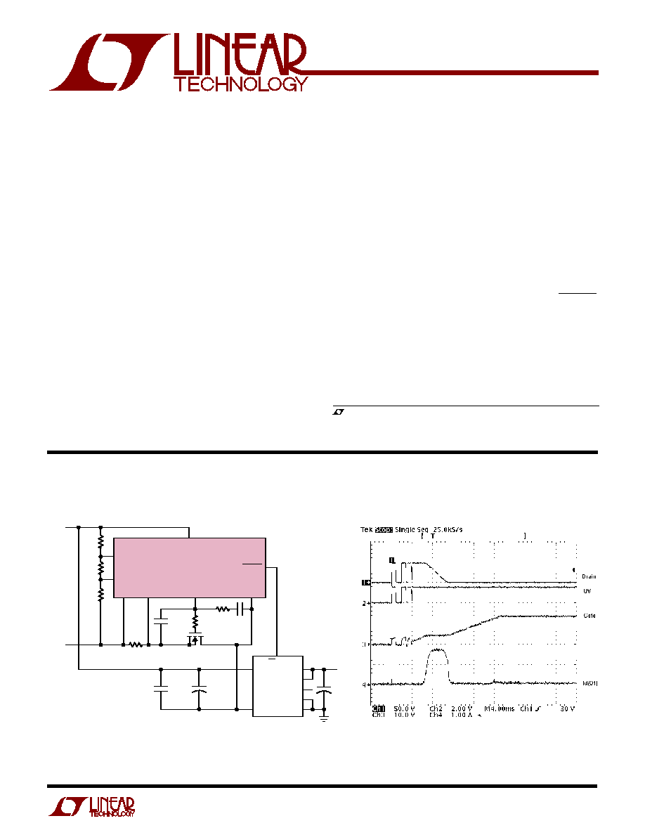
Input Inrush Current
CONTACT
BOUNCE
1640 F07b
V
EE
V
DD
LT1640L
SENSE
C1
33nF
24V
C3
0.1
µ
F
100V
C4
100
µ
F
100V
Q1
IRF530
R2
10
5%
R3
10k
5%
C2
3.3nF
100V
R4
562k
1%
R5
9.09k
1%
R6
10k
1%
R1
0.02
5%
4
OV
GND
3
2
≠ 48V
OV = 71V
UV = 37V
UV
5
6
8
7
1
GATE
DRAIN
PWRGD
1640 TA01
V
OUT
+
SENSE
+
TRIM
SENSE
≠
V
OUT
≠
V
IN
≠
ON/OFF
LUCENT
JW050A1-E
V
IN
+
2
9
5V
8
7
6
5
1
4
+
C5
100
µ
F
16V
+
2
LT1640L/LT1640H
ABSOLUTE
M
AXI
M
U
M
RATINGS
W
W
W
U
Supply Voltage (V
DD
≠ V
EE
) .................... ≠ 0.3V to 100V
DRAIN, PWRGD, PWRGD Pins ............... ≠ 0.3V to 100V
SENSE, GATE Pins .................................... ≠ 0.3V to 20V
UV, OV Pins .............................................. ≠ 0.3V to 60V
Maximum Junction Temperature ......................... 125
∞
C
Operating Temperature Range
LT1640LC/LT1640HC ............................. 0
∞
C to 70
∞
C
LT1640LI/LT1640HI .......................... ≠ 40
∞
C to 85
∞
C
Storage Temperature Range ................ ≠ 65
∞
C to 150
∞
C
Lead Temperature (Soldering, 10 sec)................. 300
∞
C
(Note 1), All Voltages Referred to V
EE
ELECTRICAL CHARACTERISTICS
SYMBOL
PARAMETER
CONDITIONS
MIN
TYP
MAX
UNITS
DC
V
DD
Supply Voltage
q
10
80
V
I
DD
Supply Current
UV = 3V, OV = V
EE
, SENSE = V
EE
q
1.3
5
mA
V
CB
Circuit Breaker Trip Voltage
V
CB
= (V
SENSE
≠ V
EE
)
q
40
50
60
mV
I
PU
GATE Pin Pull-Up Current
Gate Drive On, V
GATE
= V
EE
q
≠ 30
≠ 45
≠ 60
µ
A
I
PD
GATE Pin Pull-Down Current
Any Fault Condition
24
50
70
mA
I
SENSE
SENSE Pin Current
V
SENSE
= 50mV
≠ 20
µ
A
V
GATE
External Gate Drive
(V
GATE
≠ V
EE
), 15V
V
DD
80V
q
10
13.5
18
V
(V
GATE
≠ V
EE
), 10V
V
DD
< 15V
q
6
8
15
V
V
UVH
UV Pin High Threshold Voltage
UV Low to High Transition
q
1.213
1.243
1.272
V
V
UVL
UV Pin Low Threshold Voltage
UV High to Low Transition
q
1.198
1.223
1.247
V
V
UVHY
UV Pin Hysteresis
20
mV
I
INUV
UV Pin Input Current
V
UV
= V
EE
q
≠ 0.02
≠ 0.5
µ
A
V
OVH
OV Pin High Threshold Voltage
OV Low to High Transition
q
1.198
1.223
1.247
V
V
OVL
OV Pin Low Threshold Voltage
OV High to Low Transition
q
1.165
1.203
1.232
V
V
OVHY
OV Pin Hysteresis
20
mV
I
INOV
OV Pin Input Current
V
OV
= V
EE
q
≠ 0 .03
≠ 0.5
µ
A
(Note 2), V
DD
= 48V, V
EE
= 0V, T
A
= 25
∞
C unless otherwise noted.
W
U
U
PACKAGE/ORDER I FOR ATIO
Consult factory for Military grade parts.
ORDER PART
NUMBER
S8 PART MARKING
LT1640LCN8
LT1640LCS8
LT1640LIN8
LT1640LIS8
1640L
1640LI
T
JMAX
= 125
∞
C,
JA
= 120
∞
C/W (N8)
T
JMAX
= 125
∞
C,
JA
= 150
∞
C/W (S8)
1
2
3
4
8
7
6
5
TOP VIEW
V
DD
DRAIN
GATE
SENSE
PWRGD
OV
UV
V
EE
N8 PACKAGE
8-LEAD PDIP
S8 PACKAGE
8-LEAD PLASTIC SO
ORDER PART
NUMBER
S8 PART MARKING
LT1640HCN8
LT1640HCS8
LT1640HIN8
LT1640HIS8
1640H
1640HI
T
JMAX
= 125
∞
C,
JA
= 120
∞
C/W (N8)
T
JMAX
= 125
∞
C,
JA
= 150
∞
C/W (S8)
1
2
3
4
8
7
6
5
TOP VIEW
V
DD
DRAIN
GATE
SENSE
PWRGD
OV
UV
V
EE
N8 PACKAGE
8-LEAD PDIP
S8 PACKAGE
8-LEAD PLASTIC SO
3
LT1640L/LT1640H
ELECTRICAL CHARACTERISTICS
V
DD
= 48V, V
EE
= 0V, T
A
= 25
∞
C unless otherwise noted.
SYMBOL
PARAMETER
CONDITIONS
MIN
TYP
MAX
UNITS
V
PG
Power Good Threshold
V
DRAIN
≠ V
EE
, High to Low Transition
1.1
1.4
2.0
V
V
PGHY
Power Good Threshold Hysteresis
0.4
V
V
OL
Output Low Voltage
PWRGD (LT1640L), I
OUT
= 1mA,
q
0.48
0.8
V
(V
DRAIN
≠ V
EE
) < V
PG
R
OUT
Power Good Output Impedance
PWRGD (LT1460H), (V
DRAIN
≠ V
EE
) < V
PG
q
2
6.5
k
AC
t
PHLOV
OV High to GATE Low
Figures 1, 2
1.7
µ
s
t
PHLUV
UV Low to GATE Low
Figures 1, 3
1.5
µ
s
t
PLHOV
OV Low to GATE High
Figures 1, 2
5.5
µ
s
t
PLHUV
UV High to GATE High
Figures 1, 3
6.5
µ
s
t
PHLSENSE
SENSE High to Gate Low
Figures 1, 4
2
3
4
µ
s
t
PHLPG
DRAIN Low to PWRGD Low
(LT1640L) Figures 1, 5
0.5
µ
s
DRAIN Low to (PWRGD ≠ DRAIN) High
(LT1640H) Figures 1, 5
0.5
µ
s
t
PLHPG
DRAIN High to PWRGD High
(LT1640L) Figures 1, 5
0.5
µ
s
DRAIN High to (PWRGD ≠ DRAIN) Low
(LT1640H) Figures 1, 5
0.5
µ
s
The
q
denotes specifications which apply over the full operating
temperature range.
Note 1: Absolute Maximum Ratings are those values beyond which the life
of a device may be impaired.
Note 2: All currents into device pins are positive; all currents out of device
pins are negative. All voltages are referenced to V
EE
unless otherwise
specified.
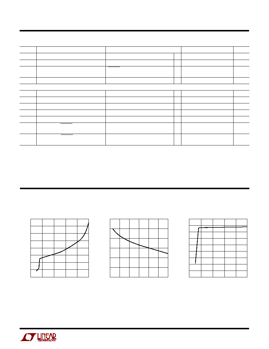
TYPICAL PERFOR A CE CHARACTERISTICS
U
W
SUPPLY VOLTAGE (V)
0
SUPPLY CURRENT (mA)
1.3
1.4
1.5
60
100
1640 G01
1.2
1.1
0
20
40
80
1.6
1.7
1.8
Supply Current vs Supply Voltage
TEMPERATURE (
∞
C)
≠ 50
≠ 25
1.0
SUPPLY CURRENT (mA)
1.1
1.2
1.3
1.4
1.6
0
25
50
75
1640 G02
100
1.5
Supply Current vs Temperature
SUPPLY VOLTAGE (V)
0
6
GATE VOLTAGE (V)
7
9
10
11
40
80
100
15
1640 G03
8
20
60
12
13
14
Gate Voltage vs Supply Voltage
4
LT1640L/LT1640H
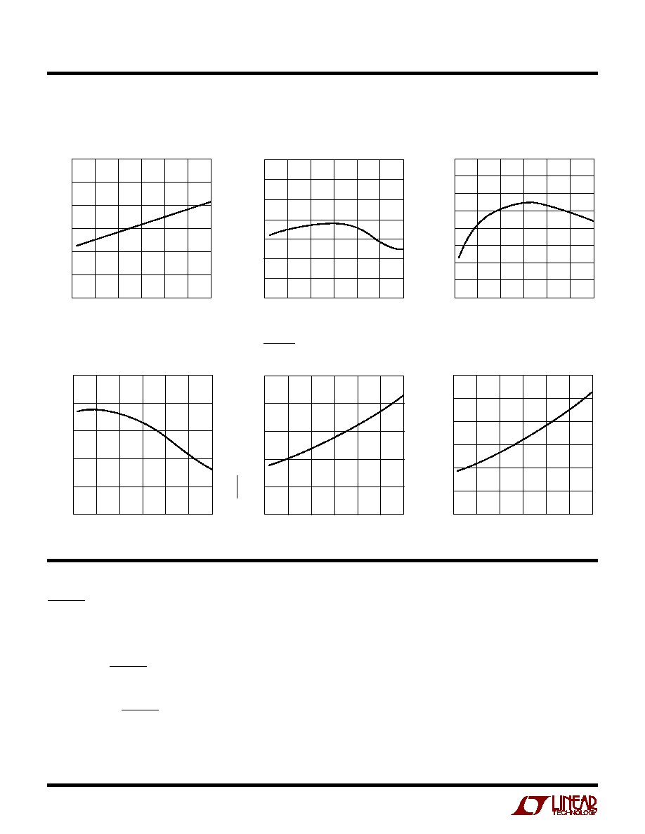
TYPICAL PERFOR A CE CHARACTERISTICS
U
W
Gate Voltage vs Temperature
TEMPERATURE (
∞
C)
12.0
GATE VOLTAGE (V) 13.0
14.0
15.0
12.5
13.5
14.5
≠ 25
0
75
1640 G04
100
≠ 50
25
50
TEMPERATURE (
∞
C)
≠ 50
48
TRIP VOLTAGE (mV)
49
51
52
53
55
25
0
50
1640 G05
50
54
100
≠ 25
75
TEMPERATURE (
∞
C)
≠ 50
GATE PULL-UP CURRENT (
µ
A)
48
47
46
45
44
43
42
41
40
75
1640 G06
≠ 25
100
50
25
0
Gate Pull-Up Current
vs Temperature
Gate Pull-Down Current
vs Temperature
TEMPERATURE (
∞
C)
≠ 50
GATE PULL-DOWN CURRENT (mA)
49
52
55
75
1640 G07
46
43
40
≠ 25
0
25
50
100
PWRGD Output Low Voltage
vs Temperature (LT1640L)
TEMPERATURE (
∞
C)
≠ 50
PWRGD OUTPUT LOW VOLTAGE (V)
0.3
0.4
0.5
75
1640 G08
0.2
0.1
0
≠ 25
25
0
50
100
TEMPERATURE (
∞
C)
≠ 50
2
OUTPUT IMPEDANCE (
)
3
4
5
6
7
8
≠ 25
25
0
50
75
1640 G09
100
PWRGD Output Impedance
vs Temperature (LT1640H)
Circuit Breaker Trip Voltage
vs Temperature
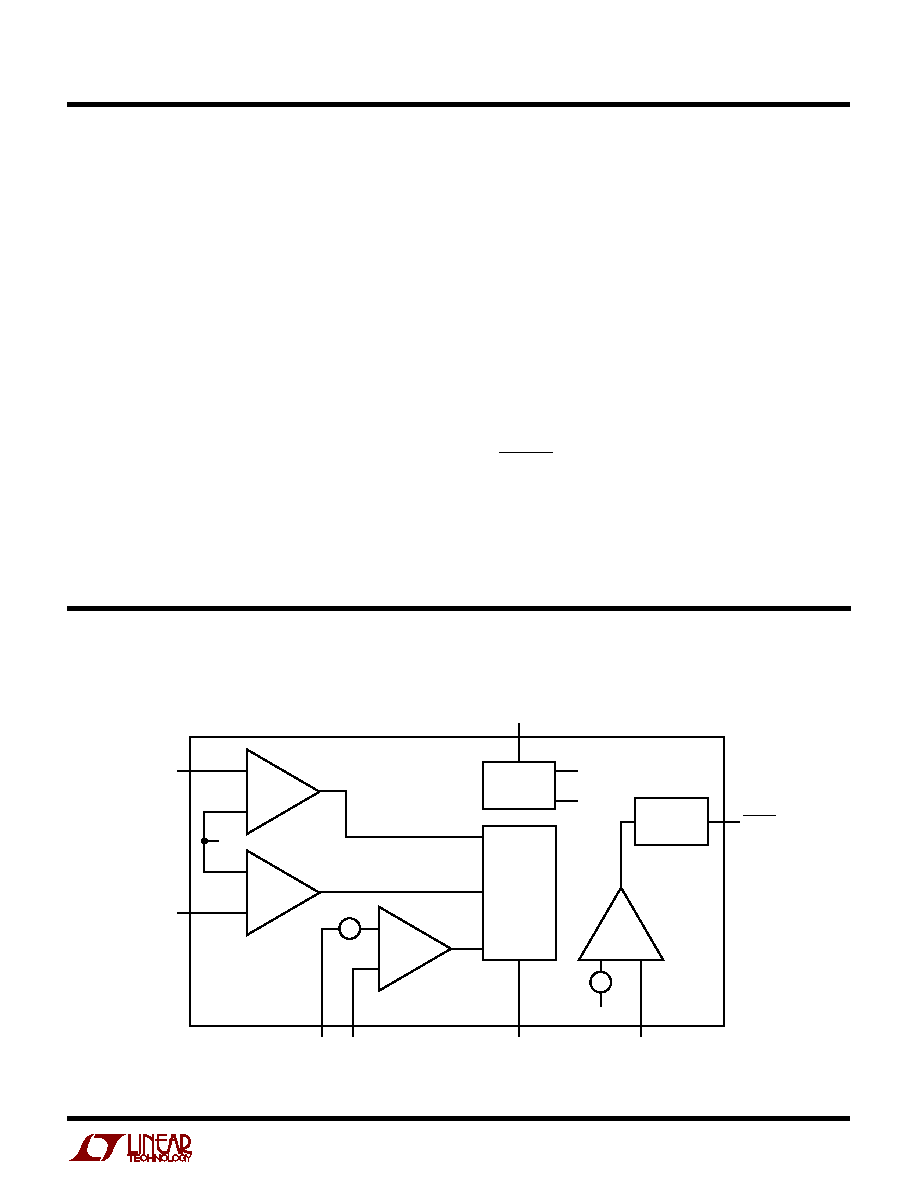
pin which pulls the module's enable pin low, forcing it off.
When V
DRAIN
drops below V
PG
, the PWRGD sink current
is turned off and a 5k resistor is connected between
PWRGD and DRAIN, allowing the module's pull-up cur-
rent to pull the enable pin high and turn on the module.
OV
(Pin 2): Analog Overvoltage Input. When OV is pulled
above the 1.223V low to high threshold, an overvoltage
condition is detected and the GATE pin will be immediately
pulled low. The GATE pin will remain low until OV drops
below the 1.203V high to low threshold.
PI
N
FU
N
CTIO
N
S
U
U
U
PWRGD/PWRGD (Pin 1): Power Good Output Pin. This pin
will toggle when V
DRAIN
is within V
PG
of V
EE
. This pin can
be connected directly to the enable pin of a power module.
When the DRAIN pin of the LT1640L is above V
EE
by more
than V
PG
, the PWRGD pin will be high impedance, allowing
the pull-up current of the module's enable pin to pull the
pin high and turn the module off. When V
DRAIN
drops
below V
PG
, the PWRGD pin sinks current to V
EE
, pulling
the enable pin low and turning on the module.
When the DRAIN pin of the LT1640H is above V
EE
by more
than V
PG
, the PWRGD pin will sink current to the DRAIN
5
LT1640L/LT1640H
PI
N
FU
N
CTIO
N
S
U
U
U
UV (Pin 3): Analog Undervoltage Input. When UV is
pulled below the 1.223V high to low threshold, an under-
voltage condition is detected and the GATE pin will be
immediately pulled low. The GATE pin will remain low
until UV rises above the 1.243 low to high threshold.
The UV pin is also used to reset the electronic circuit
breaker. If the UV pin is cycled low and high following the
trip of the circuit breaker, the circuit breaker is reset and
a normal power-up sequence will occur.
V
EE
(Pin 4): Negative Supply Voltage Input. Connect to
the lower potential of the power supply.
SENSE (Pin 5): Circuit Breaker Sense Pin. With a sense
resistor placed in the supply path between V
EE
and
SENSE, the circuit breaker will trip when the voltage
across the resistor exceeds 50mV. Noise spikes of less
than 2
µ
s are filtered out and will not trip the circuit
breaker.
If the circuit breaker trip current is set to twice the normal
operating current, only 25mV is dropped across the
sense resistor during normal operation. To disable the
circuit breaker, V
EE
and SENSE can be shorted together.
GATE (Pin 6): Gate Drive Output for the External
N-Channel. The GATE pin will go high when the following
start-up conditions are met: the UV pin is high, the OV pin
is low and (V
SENSE
≠ V
EE
) < 50mV. The GATE pin is pulled
high by a 45
µ
A current source and pulled low with a
50mA current source.
DRAIN (Pin 7): Analog Drain Sense Input. Connect this
pin to the drain of the external N-channel and the V
≠
pin
of the power module. When the DRAIN pin is below V
PG
,
the PWRGD or PWRGD pin will toggle.
V
DD
(Pin 8): Positive Supply Voltage Input. Connect this
pin to the higher potential of the power supply inputs and
the V
+
pin of the power module. The input supply voltage
ranges from 10V to 80V.
BLOCK DIAGRA
W
≠
+
≠
+
+
≠
+
≠
DRAIN
1640 BD
GATE
SENSE
V
EE
V
EE
V
PG
OUTPUT
DRIVE
PWRGD/PWRGD
50mV
V
CC
V
DD
REF
REF
UV
OV
LOGIC
AND
GATE DRIVE
V
CC
AND
REFERENCE
GENERATOR
≠
+
≠
+