 | –≠–ª–µ–∫—Ç—Ä–æ–Ω–Ω—ã–π –∫–æ–º–ø–æ–Ω–µ–Ω—Ç: LT1674CS | –°–∫–∞—á–∞—Ç—å:  PDF PDF  ZIP ZIP |

1
LT1672/LT1673/LT1674
APPLICATIO S
U
FEATURES
DESCRIPTIO
U
TYPICAL APPLICATIO
N
U
2
µ
A Max, A
V
5 Single, Dual
and Quad Over-The-Top Precision
Rail-to-Rail Input and Output Op Amps
s
Gain of 5 Stable
s
Low Supply Current: 2
µ
A Max per Amplifier
s
Rail-to-Rail Input and Output
s
Low Offset Voltage: 375
µ
V Max
s
Over-The-Top
TM
Inputs Operate Above V
+
s
Gain Bandwidth Product: 12kHz
s
Wide Supply Range: 2.2V to 36V
s
Single Supply Input Range: ≠ 0.3V to 36V
s
Low Input Bias Current: 250pA
s
Low Input Offset Current: 20pA
s
High A
VOL
: 100V/mV Minimum Driving 100k
Load
s
Output Sources and Sinks 500
µ
A Load Current
s
Reverse Battery Protected to 18V
The LT
Æ
1672/LT1673/LT1674 are ultralow power
(I
S
2
µ
A) decompensated (A
V
5) op amps with preci-
sion specifications. The extremely low supply current is
combined with excellent amplifier specifications: input
offset voltage is 375
µ
V maximum with a typical drift of
only 0.4
µ
V/
∞
C, input offset current is 100pA maximum. A
minimum open-loop gain (A
VOL
) of 100V/mV ensures that
gain errors are small. The devices' characteristics change
little over the supply range of 2.2V to
±
15V. Supply
rejection is 90dB and the common mode rejection ratio is
90dB. Operation is specified for 3V, 5V and
±
15V supplies.
Reverse battery protection (≠18V min) and inputs that
operate above the positive supply make the LT1672/
LT1673/LT1674 easy to use in harsh environments.
The low bias currents and offset current of the amplifier
permit the use of megohm level source resistors without
introducing significant errors. Voltage noise at 4
µ
V
P-P
is
remarkably low considering the low supply current. For
unity gain stable versions of these amplifiers, see the
LT1494/LT1495/LT1496.
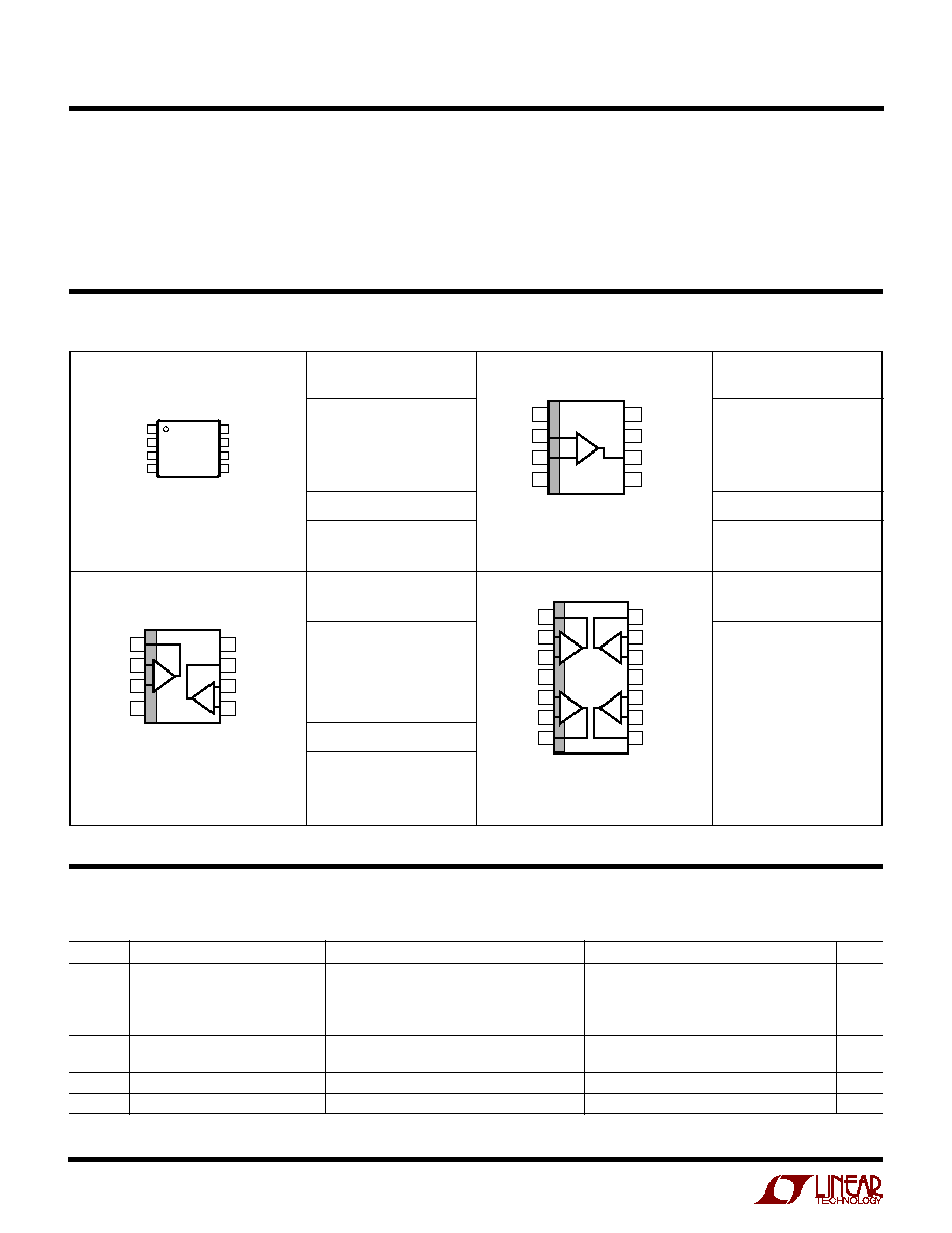
The LT1672 is available in the 8-pin MSOP, PDIP and SO
packages. The LT1673 is available in plastic 8-pin PDIP
and SO-8 packages with the standard dual op amp pinout.
The LT1674 is available in 14-pin PDIP and SO packages.
s
Battery- or Solar-Powered Systems
s
Portable Instrumentation
s
Remote Sensor Amplifier
s
Micropower Filter
s
Photodiode Amplifier
s
High Impedance Circuits
Single Supply, 60
µ
W Precision Instrumentation Amplifier
TC V
OS
Distribution
, LTC and LT are registered trademarks of Linear Technology Corporation.
100k*
100k*
5V
5V
1M
0.0047
µ
F
A
V
= 100
BANDWIDTH = 1kHz
CMRR = 65dB AT 120Hz
*500V TRANSIENT PROTECTION
TOTAL SUPPLY CURRENT = 12
µ
A
+
≠
1M
1M
100k
100k
1M
1M
V
OUT
5V
LT1389-2.5
1672/3/4 TA01
LT1672
1000pF
110k
110k
V
IN1
V
IN2
≠
+
≠
+
1/2 LT1673
1/2 LT1673
TC V
OS
(
µ
V/
∞
C)
≠1.5
UNITS
80
70
60
50
40
30
20
10
0
0.9
1672/3/4 TA02
≠ 0.9
≠ 0.3
0.3
1.5
120 AMPLIFIERS
V
S
=
±
2.5V
≠ 40
∞
C to 85
∞
C
Over-The-Top is a trademark of Linear Technology Corporation.
2
LT1672/LT1673/LT1674
S8 PART MARKING
Total Supply Voltage (V
+
to V
≠
) .............................. 36V
Differential Input Voltage ......................................... 36V
Input Current ......................................................
±
10mA
Output Short-Circuit Duration ....................... Continuous
Operating Temperature Range (Note 2) .. ≠ 40
∞
C to 85
∞
C
ORDER PART
NUMBER
T
JMAX
= 150
∞
C,
JA
= 150
∞
C/ W (N8)
T
JMAX
= 150
∞
C,
JA
= 190
∞
C/ W (S8)
1
2
3
4
8
7
6
5
TOP VIEW
OUT A
≠IN A
+IN A
V
≠
V
+
OUT B
≠IN B
+IN B
N8 PACKAGE
8-LEAD PDIP
S8 PACKAGE
8-LEAD PLASTIC SO
B
A
S8 PART MARKING
1673
1673I
LT1672CMS8
LT1672IMS8
ABSOLUTE AXI U RATI GS
W
W
W
U
PACKAGE/ORDER I FOR ATIO
U
U
W
Specified Temperature Range (Note 3) ... ≠ 40
∞
C to 85
∞
C
Storage Temperature Range ................. ≠ 65
∞
C to 150
∞
C
Junction Temperature ........................................... 150
∞
C
Lead Temperature (Soldering, 10 sec).................. 300
∞
C
(Note 1)
TOP VIEW
S PACKAGE
14-LEAD PLASTIC SO
N PACKAGE
14-LEAD PDIP
1
2
3
4
5
6
7
14
13
12
11
10
9
8
OUT A
≠IN A
+IN A
V
+
+IN B
≠IN B
OUT B
OUT D
≠IN D
+IN D
V
≠
+IN C
≠IN C
OUT C
A
B
D
C
ORDER PART
NUMBER
LT1674CN
LT1674CS
LT1674IN
LT1674IS
T
JMAX
= 150
∞
C,
JA
= 110
∞
C/ W (N)
T
JMAX
= 150
∞
C,
JA
= 150
∞
C/ W (S)
ORDER PART
NUMBER
MS8 PART MARKING
LTFH
LTFJ
LT1673CN8
LT1673CS8
LT1673IN8
LT1673IS8
1
2
3
4
NC
≠IN
+IN
V
≠
8
7
6
5
NC
V
+
OUT
NC
TOP VIEW
MS8 PACKAGE
8-LEAD PLASTIC MSOP
T
JMAX
= 150
∞
C,
JA
= 250
∞
C/ W
LT1672CN8
LT1672CS8
LT1672IN8
LT1672IS8
ORDER PART
NUMBER
1672
1672I
1
2
3
4
8
7
6
5
TOP VIEW
NC
V
+
OUT
NC
NC
≠IN
+IN
V
≠
S8 PACKAGE
8-LEAD PLASTIC SO
N8 PACKAGE
8-LEAD PDIP
T
JMAX
= 150
∞
C,
JA
= 130
∞
C/ W (N8)
T
JMAX
= 150
∞
C,
JA
= 190
∞
C/ W (S8)
Consult factory for parts specified with wider operating temperature ranges.
SYMBOL
PARAMETER
CONDITIONS
MIN
TYP
MAX
UNITS
V
OS
Input Offset Voltage
V
S
= 5V
150
375
µ
V
V
S
= 3V
200
475
µ
V
V
S
= 5V, MS8 Package
150
475
µ
V
V
S
= 3V, MS8 Package
200
575
µ
V
I
B
Input Bias Current
(Note 5)
250
1000
pA
V
CM
= 10V (Note 6)
180
360
nA
I
OS
Input Offset Current
(Note 5)
20
100
pA
Input Noise Voltage
0.1Hz to 10Hz
4
µ
V
P-P
T
A
= 25
∞
C, V
S
= 5V, 0V; V
S
= 3V, 0V; V
CM
= V
O
= half supply, unless otherwise noted.
ELECTRICAL CHARACTERISTICS

3
LT1672/LT1673/LT1674
SYMBOL
PARAMETER
CONDITIONS
MIN
TYP
MAX
UNITS
e
n
Input Noise Voltage Density
f = 100Hz
185
nV/
Hz
i
n
Input Noise Current Density
f = 100Hz
10
fA/
Hz
A
VOL
Large-Signal Voltage Gain
V
S
= 5V, V
O
= 0.25V to 4.5V, R
L
= 100k
100
500
V/mV
V
S
= 3V, V
O
= 0.25V to 2.5V, R
L
= 100k
50
250
V/mV
Input Voltage Range
0
36
V
CMRR
Common Mode Rejection Ratio
V
CM
= 0V to 4V, V
S
= 5V
90
106
dB
V
CM
= 0V to 10V, V
S
= 5V
74
95
dB
PSRR
Power Supply Rejection Ratio
V
S
= 2.2V to 12V, V
CM
= V
O
= 0.5V
90
99
dB
Minimum Operating Supply Voltage
2.1
2.2
V
V
OL
Output Voltage Swing LOW
No Load
50
100
mV
I
SINK
= 100
µ
A
210
410
mV
V
OH
Output Voltage Swing HIGH
No Load
V
+
≠ 0.07
V
+
≠ 0.035
V
I
SOURCE
= 100
µ
A
V
+
≠ 0.32
V
+
≠ 0.160
V
I
SC
Short-Circuit Current
(Note 5)
0.7
1.3
mA
I
S
Supply Current per Amplifier
(Note 6)
1.5
2
µ
A
Reverse Supply Voltage
I
S
= 10
µ
A per Amplifier
≠18
V
SR
Slew Rate
A
V
= ≠ 5, V
S
=
±
10V
1.6
5
V/ms
GBW
Gain Bandwidth Product
f = 100Hz
12
kHz
T
A
= 25
∞
C, V
S
= 5V, 0V; V
S
= 3V, 0V; V
CM
= V
O
= half supply, unless otherwise noted.
ELECTRICAL CHARACTERISTICS
The
q
denotes the specifications which apply over the temperature range of 0
∞
C
T
A
70
∞
C. V
S
= 5V, 0V; V
S
= 3V, 0V;
V
CM
= V
O
= half supply, unless otherwise noted. (Note 3)
SYMBOL
PARAMETER
CONDITIONS
MIN
TYP
MAX
UNITS
V
OS
Input Offset Voltage
V
S
= 5V
q
175
425
µ
V
V
S
= 3V
q
225
525
µ
V
V
S
= 5V, MS8 Package
q
175
525
µ
V
V
S
= 3V, MS8 Package
q
225
625
µ
V
V
OS
TC
Input Offset Voltage Drift
(Note 4)
q
0.4
2
µ
V/
∞
C
I
B
Input Bias Current
(Note 5)
q
250
1200
pA
V
CM
= 10V (Note 6)
q
240
500
nA
I
OS
Input Offset Current
(Note 5)
q
20
120
pA
A
VOL
Large-Signal Voltage Gain
V
S
= 5V, V
O
= 0.25V to 4.5V, R
L
= 100k
q
75
280
V/mV
V
S
= 3V, V
O
= 0.25V to 2.5V, R
L
= 100k
q
40
150
V/mV
Input Voltage Range
q
0.2
36
V
CMRR
Common Mode Rejection Ratio
V
CM
= 0.2V to 4V, V
S
= 5V
q
89
106
dB
V
CM
= 0.2V to 10V, V
S
= 5V
q
64
85
dB
PSRR
Power Supply Rejection Ratio
V
S
= 2.4V to 12V, V
CM
= V
O
= 0.5V
q
89
99
dB
Minimum Operating Supply Voltage
q
2.3
2.4
V
V
OL
Output Voltage Swing LOW
No Load
q
55
110
mV
I
SINK
= 100
µ
A
q
225
450
mV
V
OH
Output Voltage Swing HIGH
No Load
q
V
+
≠ 0.08
V
+
≠ 0.04
V
I
SOURCE
= 100
µ
A
q
V
+
≠ 0.36
V
+
≠ 0.18
V
I
SC
Short-Circuit Current
(Note 5)
q
0.6
1.1
mA
I
S
Supply Current per Amplifier
(Note 6)
q
1.9
2.8
µ
A

4
LT1672/LT1673/LT1674
SYMBOL
PARAMETER
CONDITIONS
MIN
TYP
MAX
UNITS
V
OS
Input Offset Voltage
200
575
µ
V
MS8 Package
200
675
µ
V
I
B
Input Bias Current
25
1000
pA
I
OS
Input Offset Current
20
100
pA
A
VOL
Large-Signal Voltage Gain
V
O
=
±
10V, R
L
= 100k
100
360
V/mV
Input Voltage Range
≠ 15
21
V
CMRR
Common Mode Rejection Ratio
V
CM
= ≠ 15V to 14V
100
120
dB
PSRR
Power Supply Rejection Ratio
V
S
=
±
5V to
±
15V
96
120
dB
V
OL
Output Voltage Swing LOW
R
L
= 1M
≠14.85
≠14.70
V
R
L
= 100k
≠14.75
≠14.50
V
V
OH
Output Voltage Swing HIGH
R
L
= 1M
14.78
14.89
V
R
L
= 100k
14.62
14.81
V
I
SC
Short-Circuit Current
0.7
1.5
mA
I
S
Supply Current per Amplifier
1.9
2.8
µ
A
SYMBOL
PARAMETER
CONDITIONS
MIN
TYP
MAX
UNITS
V
OS
Input Offset Voltage
V
S
= 5V
q
200
475
µ
V
V
S
= 3V
q
250
575
µ
V
V
S
= 5V, MS8 Package
q
200
575
µ
V
V
S
= 3V, MS8 Package
q
250
675
µ
V
V
OS
TC
Input Offset Voltage Drift
(Note 4)
q
0.4
2
µ
V/
∞
C
I
B
Input Bias Current
(Note 5)
q
250
1700
pA
V
CM
= 10V (Note 6)
q
275
750
nA
I
OS
Input Offset Current
(Note 5)
q
20
170
pA
A
VOL
Large-Signal Voltage Gain
V
S
= 5V, V
O
= 0.25V to 4.5V, R
L
= 100k
q
55
215
V/mV
V
S
= 3V, V
O
= 0.25V to 2.5V, R
L
= 100k
q
30
115
V/mV
Input Voltage Range
q
0.2
36
V
CMRR
Common Mode Rejection Ratio
V
CM
= 0.2V to 4V, V
S
= 5V
q
88
106
dB
V
CM
= 0.2V to 10V, V
S
= 5V
q
62
75
dB
PSRR
Power Supply Rejection Ratio
V
S
= 2.7V to 12V, V
CM
= V
O
= 0.5V
q
88
99
dB
Minimum Operating Supply Voltage
q
2.6
2.7
V
V
OL
Output Voltage Swing LOW
No Load
q
60
120
mV
I
SINK
= 100
µ
A
q
245
490
mV
V
OH
Output Voltage Swing HIGH
No Load
q
V
+
≠ 0.10
V
+
≠ 0.05
mV
I
SOURCE
= 100
µ
A
q
V
+
≠ 0.38
V
+
≠ 0.19
mV
I
SC
Short-Circuit Current
(Note 5)
q
0.4
0.9
mA
I
S
Supply Current per Amplifier
(Note 6)
q
2.1
3.1
µ
A
The
q
denotes the specifications which apply over the temperature range of ≠ 40
∞
C
T
A
85
∞
C. V
S
= 5V, 0V; V
S
= 3V, 0V;
V
CM
= V
O
= half supply, unless otherwise noted. (Note 3)
ELECTRICAL CHARACTERISTICS
T
A
= 25
∞
C, V
S
=
±
15V, V
CM
= V
O
= 0V, unless otherwise noted.

5
LT1672/LT1673/LT1674
SYMBOL
PARAMETER
CONDITIONS
MIN
TYP
MAX
UNITS
V
OS
Input Offset Voltage
q
250
675
µ
V
MS8 Package
q
250
775
µ
V
I
B
Input Bias Current
q
250
1700
pA
I
OS
Input Offset Current
q
20
170
pA
A
VOL
Large-Signal Voltage Gain
V
O
=
±
10V, R
L
= 100k
q
50
200
V/mV
Input Voltage Range
q
≠ 14.8
21
V
CMRR
Common Mode Rejection Ratio
V
CM
= ≠14.8V to 14V
q
96
114
dB
PSRR
Power Supply Rejection Ratio
V
S
=
±
5V to
±
15V
q
92
120
dB
V
OL
Output Voltage Swing LOW
R
L
= 1M
q
≠14.83
≠14.66
V
R
L
= 100k
q
≠14.72
≠14.44
V
V
OH
Output Voltage Swing HIGH
R
L
= 1M
q
14.74
14.87
V
R
L
= 100k
q
14.54
14.77
V
I
SC
Short-Circuit Current
q
0.4
1.1
mA
I
S
Supply Current per Amplifier
q
2.8
4.2
µ
A
ELECTRICAL CHARACTERISTICS
Note 1: Absolute Maximum Ratings are those values beyond which the life
of the device may be impaired.
Note 2: The LT1672C/LT1673C/LT1674C and LT1672I/LT1673I/LT1674I
are guaranteed functional over the Operating Temperature Range of ≠ 40
∞
C
to 85
∞
C.
Note 3: The LT1672C/LT1673C/LT1674C are guaranteed to meet specified
performance from 0
∞
C to 70
∞
C. The LT1672C/LT1673C/LT1674C are
designed, characterized and expected to meet specified performance from
≠ 40
∞
C to 85
∞
C but are not tested or QA sampled at these temperatures.
The LT1672I/LT1673I/LT1674I are guaranteed to meet specified
performance from ≠ 40
∞
C to 85
∞
C.
Note 4: This parameter is not 100% tested.
Note 5: V
S
= 5V limit guaranteed by correlation to V
S
= 3V and V
S
=
±
15V
tests.
Note 6: V
S
= 3V limit guaranteed by correlation to V
S
= 5V and V
S
=
±
15V
tests.
The
q
denotes the specifications which apply over the temperature range of ≠40
∞
C
T
A
85
∞
C, V
S
=
±
15V, V
CM
= V
O
= 0V,
unless otherwise noted. (Note 3)
SYMBOL
PARAMETER
CONDITIONS
MIN
TYP
MAX
UNITS
V
OS
Input Offset Voltage
q
225
625
µ
V
MS8 Package
q
225
725
µ
V
I
B
Input Bias Current
q
250
1200
pA
I
OS
Input Offset Current
q
20
120
pA
A
VOL
Large-Signal Voltage Gain
V
O
=
±
10V, R
L
= 100k
q
60
240
V/mV
Input Voltage Range
q
≠ 14.8
21
V
CMRR
Common Mode Rejection Ratio
V
CM
= ≠14.8V to 14V
q
98
120
dB
PSRR
Power Supply Rejection Ratio
V
S
=
±
5V to
±
15V
q
94
120
dB
V
OL
Output Voltage Swing LOW
R
L
= 1M
q
≠14.84
≠14.67
V
R
L
= 100k
q
≠14.73
≠14.46
V
V
OH
Output Voltage Swing HIGH
R
L
= 1M
q
14.76
14.88
V
R
L
= 100k
q
14.58
14.79
mV
I
SC
Short-Circuit Current
q
0.6
1.3
mA
I
S
Supply Current per Amplifier
q
2.4
3.5
µ
A
The
q
denotes the specifications which apply over the temperature range of 0
∞
C
T
A
70
∞
C, V
S
=
±
15V, V
CM
= V
O
= 0V,
unless otherwise noted. (Note 3)