Äîêóìåíòàöèÿ è îïèñàíèÿ www.docs.chipfind.ru
1
LT1675/LT1675-1
250MHz, Triple and Single
RGB Multiplexer with Current Feedback Amplifiers
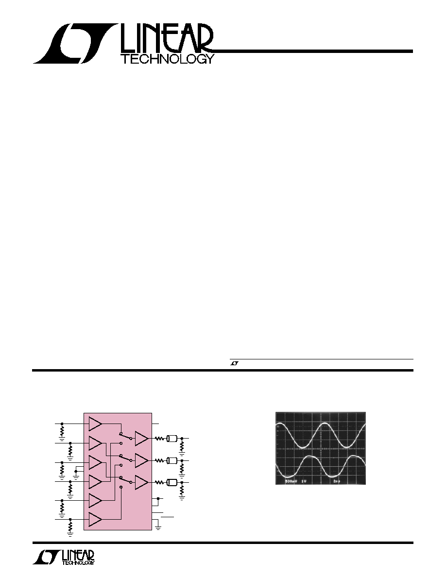
RED 1
GREEN 1
BLUE 1
RED 2
GREEN 2
BLUE 2
75
75
75
75
CABLE
CABLE
CABLE
V
+
V
SELECT RGB1/RGB2
1675 TA01
ENABLE
75
75
75
75
75
75
V
OUT RED
75
LT1675
75
V
OUT GREEN
V
OUT BLUE
+1
+1
+2
+2
+2
+1
+1
+1
+1
TYPICAL APPLICATIO
N
U
High Speed RGB MUX
FEATURES
s
RGB Switching
s
Workstation Graphics
s
Pixel Switching
s
Coaxial Cable Drivers
s
High Speed Signal Processing
APPLICATIO
N
S
U
The LT
®
1675 is a high speed RGB multiplexer designed for
pixel switching and fast workstation graphics.
Included on chip are three SPDT switches and three
current feedback amplifiers. The current feedback ampli-
fiers drive double-terminated 50
or 75
cables and are
DESCRIPTIO
N
U
s
100MHz Pixel Switching
s
3dB Bandwidth: 250MHz
s
Small 16-Pin SSOP Package
s
Channel Switching Time: 2.5ns
s
Expandable to Larger Arrays
s
Drives Cables Directly
s
High Slew Rate: 1100V/
µ
s
s
Low Switching Transient: 50mV
s
Shutdown Supply Current: 0mA
s
Output Short-Circuit Protected
configured for a fixed gain of 2, eliminating six external
gain setting resistors. The SPDT switches are designed to
be break-before-make to minimize unwanted signals cou-
pling to the input.
The LT1675-1 is a single version with two inputs, a single
output and is ideal for a single channel application such as
video sync.
The key to the LT1675 fast switching speed is Linear
Technology's proprietary high speed bipolar process. This
MUX can toggle between sources in excess of 100MHz,
has a slew rate over 1000V/
µ
s and has a 3dB bandwidth
of 250MHz. The speed and ease of use of the LT1675 make
it ideal for high performance PCs, workstations and pro-
fessional video monitors. The input-referred switching
transient is only 50mV
P-P
and lasts just 5ns, making it
virtually undetectable. Power supply requirements are
±
4V to
±
6V and power dissipation is only 300mW on
±
5V,
or 100mW for the LT1675-1. The expandable feature uses
the disable pin to reduce the power dissipation to near
0mW in the off parts.
Unlike competitive solutions that are in bulky high pin
count packages, the LT1675 is in a 16-lead narrow body
SSOP. This small footprint, the size of an SO-8, results in
a very clean high performance solution. The LT1675-1 is
available in the tiny MSOP and the SO-8.
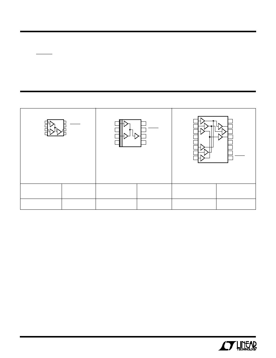
RED 1 = 0V, RED 2 = 1V, R
L
= 100
MEASURED BETWEEN 50
BACK TERMINATION AND 50
LOAD
500mV/DIV
1V/DIV
1675 TA02
0V
RED
OUT
1V
0V
SELECT
LOGIC
PIN 10
3V
Select Pin Switches Inputs at 100MHz
, LTC and LT are registered trademarks of Linear Technology Corporation.
2
LT1675/LT1675-1
ABSOLUTE
M
AXI
M
U
M
RATINGS
W
W
W
U
Supply Voltage .....................................................
±
6.3V
Inputs, ENABLE and SELECT, Current ................
±
20mA
Output Short-Circuit Duration (Note 2) ......... Continuous
Specified Temperature Range (Note 3) ....... 0
°
C to 70
°
C
Operating Temperature Range ................ 40
°
C to 85
°
C
Storage Temperature Range ................. 65
°
C to 150
°
C
Junction Temperature (Note 4) ............................ 150
°
C
Lead Temperature (Soldering, 10 sec).................. 300
°
C
(Note 1)
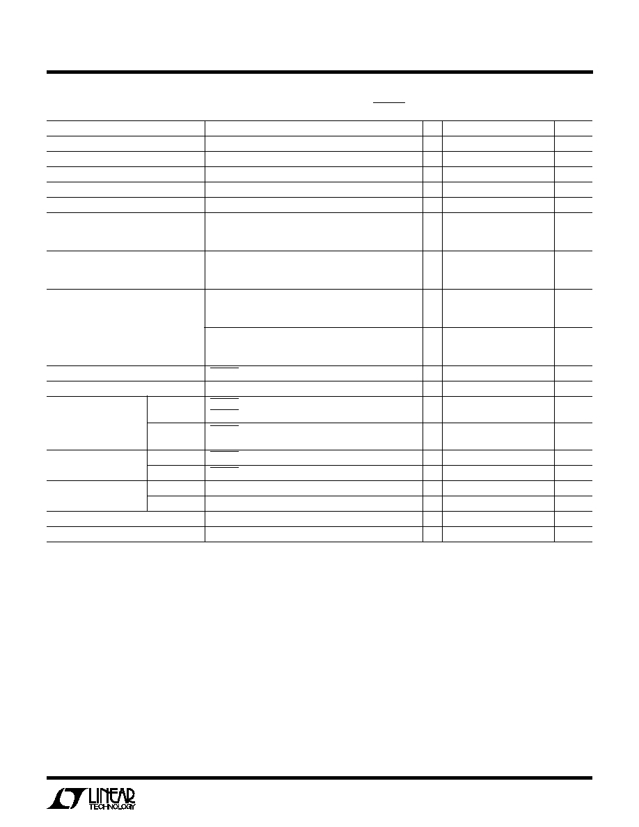
PACKAGE/ORDER I
N
FOR
M
ATIO
N
W
U
U
1
2
3
4
5
6
7
8
TOP VIEW
GN PACKAGE
16-LEAD PLASTIC SSOP NARROW
16
15
14
13
12
11
10
9
V
+
V
OUT RED
V
OUT GREEN
V
OUT BLUE
V
V
SELECT
ENABLE
RED 1
GREEN 1
BLUE 1
GND
GND
RED 2
GREEN 2
BLUE 2
T
JMAX
= 150
°
C,
JA
= 120
°
C/ W
T
JMAX
= 150
°
C,
JA
= 250
°
C/ W
T
JMAX
= 150
°
C,
JA
= 150
°
C/ W
LT1675CMS8-1
1
2
3
4
V
IN1
GND
V
IN2
V
8
7
6
5
V
+
ENABLE
V
OUT
SELECT
TOP VIEW
MS8 PACKAGE
8-LEAD PLASTIC MSOP
1
2
3
4
8
7
6
5
TOP VIEW
V
+
ENABLE
V
OUT
SELECT
V
IN1
GND
V
IN2
V
S8 PACKAGE
8-LEAD PLASTIC SO
MS8 PART
MARKING
LTGX
S8 PART
MARKING
16751
ORDER PART
NUMBER
LT1675CS8-1
ORDER PART
NUMBER
Consult factory for Industrial and Military grade parts.
GN PART
MARKING
1675
ORDER PART
NUMBER
LT1675CGN
3
LT1675/LT1675-1
ELECTRICAL CHARACTERISTICS
PARAMETER
CONDITIONS
MIN
TYP
MAX
UNITS
Output Offset Voltage
Any Input Selected
q
20
40
mV
Output Offset Matching
Between Outputs R1 to R2, G1 to G2, B1 to B2
q
5
20
mV
Input Current
Any Input Selected
q
12
30
µ
A
Input Resistance
V
IN
=
±
1V
q
100
700
k
PSRR
V
S
=
±
2.6V to
±
6V, Measured at Output
q
38
50
dB
DC Gain Error 0V to 1V
V
IN
= 1V, R
L
=
q
3
6
%
V
IN
= 1V, R
L
= 150
q
4
8
%
V
IN
= 1V, R
L
= 75
q
5
10
%
DC Gain Error 0V to 1V
V
IN
= 1V, R
L
=
q
3
6
%
V
IN
= 1V, R
L
= 150
q
4
8
%
V
IN
= 1V, R
L
= 75
q
8
20
%
Output Voltage
V
IN
= 2V, R
L
=
q
3.1
3.4
V
V
IN
= 2V, R
L
= 150
q
2.8
3.0
V
V
IN
= 2V, R
L
= 75
q
2.4
2.8
V
V
IN
= 2V, R
L
=
q
3.1
3.3
V
V
IN
= 2V, R
L
= 150
q
2.7
3.0
V
V
IN
= 2V, R
L
= 75
q
2.3
2.6
V
Disabled Output Impedance
ENABLE Open
q
1.1
1.5
2.0
k
Maximum Output Current
V
IN
=
±
1V, V
O
= 0V
q
50
70
mA
Supply Current
LT1675
ENABLE = 0V
q
25
33
42
mA
ENABLE = 4.7V
q
1
100
µ
A
LT1675-1
ENABLE = 0V
q
8
11
14
mA
ENABLE = 4.7V
q
0.3
33
µ
A
ENABLE Pin Current
LT1675
ENABLE= 0V
q
450
600
µ
A
LT1675-1
ENABLE= 0V
q
150
200
µ
A
SELECT Pin Current
LT1675
SELECT = 0V
q
90
180
µ
A
LT1675-1
SELECT = 0V
q
30
60
µ
A
SELECT Low
SELECT (See Truth Table)
q
0.8
V
SELECT High
SELECT (See Truth Table)
q
2
V
0
°
C
T
A
70
°
C, V
S
=
±
5V, R
L
=
,
V
IN
= 0V LT1675 (Pins 1, 2, 3, 6, 7, 8),
LT1675-1 (Pins 1, 3), ENABLE = 0V, unless otherwise specified.
4
LT1675/LT1675-1
AC CHARACTERISTICS
PARAMETER
CONDITIONS
MIN
TYP
MAX
UNITS
Slew Rate
V
OUT
= 5V
P-P
1100
V/
µ
s
Full Power Bandwidth (Note 5)
V
OUT
=6V
P-P
58
MHz
Small-Signal 3dB Bandwidth
Less Than 1dB Peaking
250
MHz
Gain Flatness
Less Than 0.1dB
70
MHz
Gain Matching
R to G to B
0.10
dB
R1 to R2, G1 to G2, B1 to B2, LT1675-1 V
IN1
to V
IN2
0.01
dB
Channel-to-Channel Select Time
R1 = 0V, R2 = 1V
Delay Time
Measured from Time SELECT Pin Crosses Logic Threshold
5.0
ns
Switching Time
Time for V
OUT
to Go from 0V to 1V
2.5
ns
Enable Time
10
ns
Disable Time
100
ns
Input Pin Capacitance
2
pF
SELECT Pin Capacitance
LT1675
2.2
pF
LT1675-1
1.5
pF
ENABLE Pin Capacitance
LT1675
2.1
pF
LT1675-1
1.5
pF
Output Pin Capacitance (Disabled)
ENABLE Open
4.4
pF
Small-Signal Rise Time
V
IN
= 300mV
P-P
, R
L
= 100
1.85
ns
Propagation Delay
V
IN
= 300mV
P-P
, R
L
= 100
3
ns
Overshoot
V
IN
= 300mV
P-P
, R
L
= 100
10
%
On-Channel to Off-Channel Crosstalk
Measured at 10MHz
60
dB
Chip Disable Crosstalk
Measured at 10MHz, ENABLE Open
90
dB
Channel Select Output Transient
Measured Between Back Termination and Load
50
mV
P-P
Differential Gain (Note 6)
0.07
%
Differential Phase (Note 6)
0.05
DEG
Note 4: T
J
is calculated from the ambient temperature T
A
and power
dissipation P
D
according to the following formula:
LT1675CGN: T
J
= T
A
+ (P
D
)(120
°
C/W)
LT1675CMS8-1: T
J
= T
A
+ (P
D
)(250
°
C/W)
LT1675CS8-1: T
J
= T
A
+ (P
D
)(150
°
C/W)
Note 5: Full power bandwidth is calculated from the slew rate
measurement:
FPBW = SR/2
V
PEAK
.
Note 6: Differential Gain and Phase are measured using a Tektronix
TSG120 YC/NTSC signal generator and a Tektronix 1780R Video
Measurement Set. The resolution of this equipment is 0.1% and 0.1
°
. Nine
identical MUXs were cascaded giving an effective resolution of 0.011%
and 0.011
°
.
The
q
denotes specifications that apply over the specified temperature
range.
Note 1: Absolute Maximum Ratings are those values beyond which the life
of a device may be impaired.
Note 2: May require a heat sink.
Note 3: The LT1675/LT1675-1 are guaranteed to meet specified
performance from 0
°
C to 70
°
C and are designed, characterized and
expected to meet these extended temperature limits, but are not tested at
40
°
C and 85
°
C. Guaranteed I grade parts are available; consult factory.
Truth Table
LT1675
LT1675-1
SELECT
ENABLE
RED OUT
GREEN OUT
BLUE OUT
VOUT
1
0
RED 1
GREEN 1
BLUE 1
VIN1
0
0
RED 2
GREEN 2
BLUE 2
VIN2
X
1
OFF
OFF
OFF
OFF
0
°
C
T
A
70
°
C, V
S
=
±
5V, R
L
= 150
,
V
IN
= 0V LT1675 (Pins 1, 2, 3, 6, 7, 8),
LT1675-1 (Pins 1, 3), ENABLE = 0V, unless otherwise specified.
5
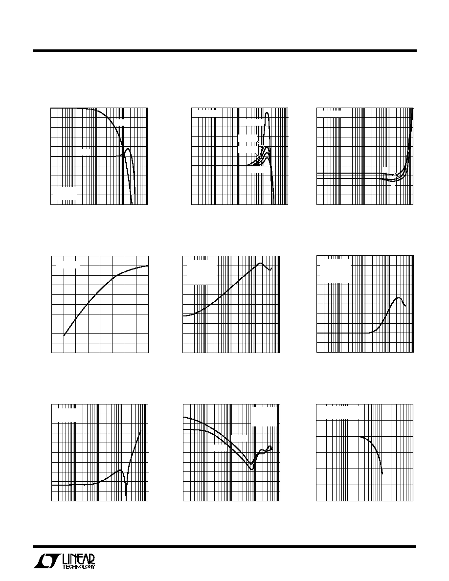
LT1675/LT1675-1
TYPICAL PERFOR
M
A
N
CE CHARACTERISTICS
U
W
FREQUENCY (Hz)
GAIN (dB)
6.5
6.4
6.3
6.2
6.1
6.0
5.9
5.8
5.7
5.6
5.5
10k
1M
10M
100M
1675 G03
100k
R
L
= 100
R G
B
Gain vs Frequency
FREQUENCY (Hz)
GAIN (dB)
6
5
4
3
2
1
0
1
2
3
4
100k
10M
100M
1G
1675 G02
1M
C
L
= 5pF
C
L
= 3pF
C
L
= 10pF
R
L
= 150
C
L
= 0pF
Frequency Response with
Capacitive Loads
FREQUENCY (Hz)
CROSSTALK REJECTION (dB)
20
10
0
10
20
30
40
50
60
70
80
100k
10M
100M
1G
1675 G23
1M
R
S
= 75
R
L
= 150
G1 DRIVEN
R1 SELECTED
Crosstalk Rejection vs Frequency
Crosstalk Rejection vs Frequency
(Disabled)
3dB Bandwidth vs
Supply Voltage
SUPPLY VOLTAGE (
±
V)
2
FREQUENCY (MHz)
300
280
260
240
220
200
180
160
140
120
100
3
4
1675 G04
5
6
R
L
= 150
FREQUENCY (Hz)
GAIN (dB)
PHASE (DEG)
5
4
3
2
1
0
1
2
3
4
5
0
20
40
60
80
100
120
140
160
180
200
100k
10M
100M
1G
1675 G01
1M
PHASE
GAIN
C
L
= 0pF
R
L
= 150
Gain and Phase vs
Frequency
FREQUENCY (Hz)
1M
OUTPUT VOLTAGE (V
P-P
)
8
7
6
5
4
3
2
10M
100M
1G
1675 G08
V
S
=
±
5V
R
L
= 150
Undistorted Output Swing
vs Frequency
FREQUENCY (Hz)
CROSSTALK REJECTION (dB)
30
40
50
60
70
80
90
100
110
120
130
100k
10M
100M
1G
1675 G05
1M
R
S
= 75
R
L
= 150
R1 DRIVEN
R2 SELECTED
Crosstalk Rejection vs Frequency
Power Supply Rejection Ratio
vs Frequency
FREQUENCY (Hz)
CROSSTALK REJECTION (dB)
10
20
30
40
50
60
70
80
90
100
110
100k
10M
100M
1G
1675 G06
1M
R
S
= 75
R
L
= 150
FREQUENCY (Hz)
POWER SUPPLY REJECTION RATIO (dB)
70
60
50
40
30
20
10
0
10
20
30
100k
10M
100M
1G
1675 G07
1M
PSRR
+PSRR
V
S
=
±
5V
T
A
= 25
°
C
R
L
= 150