 | ÐлекÑÑоннÑй компоненÑ: LT1677C | СкаÑаÑÑ:  PDF PDF  ZIP ZIP |
Äîêóìåíòàöèÿ è îïèñàíèÿ www.docs.chipfind.ru
1
LT1677
Low Noise, Rail-to-Rail
Precision Op Amp
February 2000
s
Rail-to-Rail Input and Output
s
100% Tested Low Voltage Noise:
3.2nV/
Hz Typ at 1kHz
4.5nV/
Hz Max at 1kHz
s
Offset Voltage: 60
µ
V Max
s
Low V
OS
Drift: 0.2
µ
V/
°
C Typ
s
Low Input Bias Current: 20nA Max
s
Wide Supply Range: 3V to
±
15V
s
High A
VOL
: 4V/
µ
V Min, R
L
= 1k
s
High CMRR: 109dB Min
s
High PSRR: 108dB Min
s
Gain Bandwidth Product: 7.2MHz
s
Slew Rate: 2.5V/
µ
s
s
Operating Temperature Range: 40
°
C to 85
°
C
The LT
®
1677 features the lowest noise performance avail-
able for a rail-to-rail operational amplifier: 3.2nV/
Hz
wideband noise, 1/f corner frequency of 13Hz and 70nV
peak-to-peak 0.1Hz to 10Hz noise. Low noise is combined
with outstanding precision: 20
µ
V offset voltage and
0.2
µ
V/
°
C drift, 130dB common mode and power supply
rejection and 7.2MHz gain bandwidth product. The com-
mon mode range exceeds the power supply by 100mV.
The voltage gain of the LT1677 is extremely high, especially
with a single supply: 20 million driving a 1k load.
In the design, processing and testing of the device, particular
attention has been paid to the optimization of the entire
distribution of several key parameters. Consequently, the
specifications of even the lowest cost grade have been
spectacularly improved compared to competing rail-to-rail
amplifiers.
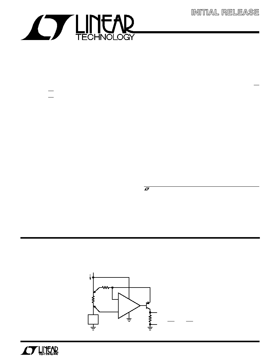
Precision High Side Current Sense
s
Low Noise Signal Processing
s
Microvolt Accuracy Threshold Detection
s
Strain Gauge Amplifiers
s
Tape Head Preamplifiers
s
Direct Coupled Audio Gain Stages
s
Infrared Detectors
+
LT1677
2
7
ZETEX
BC856B
V
OUT
1677 TA01
4
6
3
R
IN
1k
SOURCE
R
LINE
0.1
R
OUT
20k
LOAD
V
OUT
I
LOAD
= R
LINE
= 2V/AMP
R
OUT
R
IN
, LTC and LT are registered trademarks of Linear Technology Corporation.
Final Electrical Specifications
Information furnished by Linear Technology Corporation is believed to be accurate and reliable.
However, no responsibility is assumed for its use. Linear Technology Corporation makes no represen-
tation that the interconnection of its circuits as described herein will not infringe on existing patent rights.
FEATURES
DESCRIPTIO
U
APPLICATIO S
U
TYPICAL APPLICATIO
U
2
LT1677
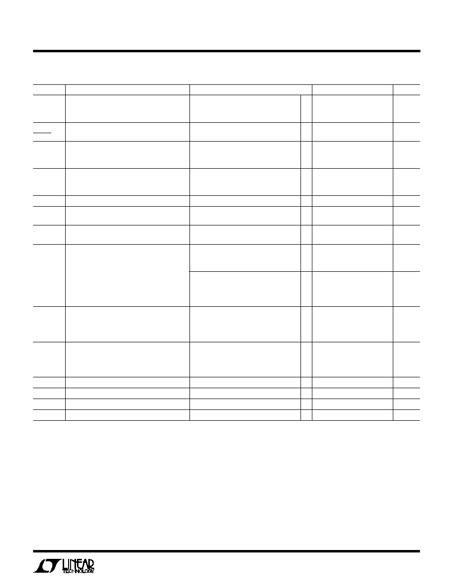
SYMBOL
PARAMETER
CONDITIONS (Note 6)
MIN
TYP
MAX
UNITS
V
OS
Input Offset Voltage
20
60
µ
V
V
CM
= 14V to 15.1V
150
400
µ
V
V
CM
= 13.3V to 15.1V
1.5
5
mV
V
OS
Long Term Input Voltage Stability
0.3
µ
V/Mo
Time
I
B
Input Bias Current
±
2
±
20
nA
V
CM
= 14V to 15.1V
0.16
0.4
µ
A
V
CM
= 13.3V to 15.1V
1.5
0.4
µ
A
I
OS
Input Offset Current
3
15
nA
V
CM
= 14V to 15.1V
5
25
nA
V
CM
= 13.3V to 15.1V
20
200
nA
e
n
Input Noise Voltage
0.1Hz to 10Hz (Note 7)
70
nV
P-P
V
CM
= 15V
33
nV
P-P
V
CM
= 15V
100
nV
P-P
Input Noise Voltage Density
V
CM
= 0V, f
O
= 10Hz
5.2
nV/
Hz
V
CM
= 15V, f
O
= 10Hz
25
nV/
Hz
V
CM
= 15V, f
O
= 10Hz
7
nV/
Hz
V
CM
= 0V, f
O
= 1kHz (Note 8)
3.2
4.5
nV/
Hz
V
CM
= 15V, f
O
= 1kHz
17
nV/
Hz
V
CM
= 15V, f
O
= 1kHz
5.3
nV/
Hz
Supply Voltage ......................................................
±
22V
Input Voltages (Note 2) ............ 0.3V Beyond Either Rail
Differential Input Current (Note 2) .....................
±
25mA
Output Short-Circuit Duration (Note 3) ............ Indefinite
Storage Temperature Range ................. 65
°
C to 150
°
C
Lead Temperature (Soldering, 10 sec.)................. 300
°
C
ORDER PART
NUMBER
T
A
= 25
°
C, V
S
=
±
15V, V
CM
= V
O
= 0V unless otherwise noted.
LT1677CN8
LT1677IN8
T
JMAX
= 150
°
C,
JA
= 130
°
C/ W
Operating Temperature Range
LT1677C (Note 4) ............................. 40
°
C to 85
°
C
LT1677I ............................................. 40
°
C to 85
°
C
Specified Temperature Range
LT1677C (Note 5) ............................. 40
°
C to 85
°
C
LT1677I ............................................. 40
°
C to 85
°
C
1
2
3
4
8
7
6
5
TOP VIEW
V
OS
TRIM
V
OS
TRIM
V
+
OUT
NC
IN
+IN
V
+
N8 PACKAGE
8-LEAD PDIP
ORDER PART
NUMBER
LT1677CS8
LT1677IS8
S8 PART MARKING
1677
1677I
TOP VIEW
S8 PACKAGE
8-LEAD PLASTIC SO
1
2
3
4
8
7
6
5
V
OS
TRIM
V
OS
TRIM
V
+
OUT
NC
IN
+IN
V
+
T
JMAX
= 150
°
C,
JA
= 190
°
C/ W
(Note 1)
Consult factory for Military grade parts.
ABSOLUTE AXI U RATI GS
W
W
W
U
PACKAGE/ORDER I FOR ATIO
U
U
W
ELECTRICAL CHARACTERISTICS
3
LT1677
SYMBOL
PARAMETER
CONDITIONS (Note 6)
MIN
TYP
MAX
UNITS
i
n
Input Noise Current Density
f
O
= 10Hz
1.2
pA/
Hz
f
O
= 1kHz
0.3
pA/
Hz
V
CM
Input Voltage Range
±
15.1
±
15.2
V
R
IN
Input Resistance
Common Mode
2
G
C
IN
Input Capacitance
3.8
pF
V
S
=
±
2.5V
4.2
pF
CMRR
Common Mode Rejection Ratio
V
CM
= 13.3V to 14.0V
109
130
dB
V
CM
=
±
15.1V
74
95
dB
PSRR
Power Supply Rejection Ratio
V
S
=
±
1.7V to
±
18V
106
130
dB
V
S
= 2.7V to 40V, V
CM
= V
O
= 1.7V
108
125
dB
A
VOL
Large-Signal Voltage Gain
R
L
10k, V
O
=
±
14V
7
25
V/
µ
V
R
L
1k, V
O
=
±
13.5V
4
20
V/
µ
V
R
L
600
, V
O
=
±
10V
0.4
0.7
V/
µ
V
V
CC
= 5V or 3V, V
EE
= 0V, V
CM
= 1.7V,
R
L
to GND, V
OUT
= 0.5V to:
R
L
10k, V
CC
0.5V
2
10
V/
µ
V
R
L
1k, V
CC
0.7V
1.5
4
V/
µ
V
V
OL
Output Voltage Swing Low
Above V
EE
I
SINK
= 0.1mA
80
170
mV
I
SINK
= 2.5mA
110
250
mV
I
SINK
= 10mA
300
500
mV
V
OH
Output Voltage Swing High
Below V
CC
I
SOURCE
= 0.1mA
110
170
mV
I
SOURCE
= 2.5mA
190
300
mV
I
SOURCE
= 10mA
500
700
mV
I
SC
Output Short-Circuit Current (Note 3)
25
35
mA
SR
Slew Rate
R
L
10k (Note 9)
1.7
2.5
V/
µ
s
GBW
Gain Bandwidth Product
f
O
= 100kHz
4.5
7.2
MHz
THD
Total Harmonic Distortion
R
L
= 2k, A
V
= 1, f
O
= 1kHz, V
O
= 10V
P-P
0.0006
%
t
S
Settling Time
10V Step 0.1%, A
V
= +1
5
µ
s
10V Step 0.01%, A
V
= +1
6
µ
s
R
O
Open-Loop Output Resistance
I
OUT
= 0
80
Closed-Loop Output Resistance
A
V
= 100, f = 10kHz
1
I
S
Supply Current
2.75
3.5
mA
T
A
= 25
°
C, V
S
=
±
15V, V
CM
= V
O
= 0V unless otherwise noted.
ELECTRICAL CHARACTERISTICS
4
LT1677
SYMBOL
PARAMETER
CONDITIONS (Note 6)
MIN
TYP
MAX
UNITS
V
OS
Input Offset Voltage
q
30
120
µ
V
V
CM
= 14.0V to 14.8V
q
180
550
µ
V
V
CM
= 13.3V to 15V
q
1.8
6
mV
V
OS
Average Input Offset Drift
SO-8
q
0.40
2
µ
V/
°
C
Temp
N8 (Note 10)
q
0.20
0.5
µ
V/
°
C
I
B
Input Bias Current
q
±
3
±
35
nA
V
CM
= 14.0V to 14.8V
q
0.19
0.6
µ
A
V
CM
= 13.3V to 15V
q
2
0.43
µ
A
I
OS
Input Offset Current
q
2
20
nA
V
CM
= 14.0V to 14.8V
q
90
220
nA
V
CM
= 13.3V to 15V
q
90
350
nA
V
CM
Input Voltage Range
q
15
14.8
V
CMRR
Common Mode Rejection Ratio
V
CM
= 13.3V to 14.0V
q
106
126
dB
V
CM
= 15V to 14.8V
q
73
93
dB
PSRR
Power Supply Rejection Ratio
V
S
=
±
1.7V to
±
18V
q
104
127
dB
V
S
= 2.8V to 40V, V
CM
= V
O
= 1.7V
q
106
122
dB
A
VOL
Large-Signal Voltage Gain
R
L
10k, V
O
=
±
14V
q
4
20
V/
µ
V
R
L
1k, V
O
=
±
13.5V
q
2
10
V/
µ
V
R
L
600
, V
O
=
±
10V
q
0.3
0.5
V/
µ
V
V
CC
= 5V or 3V, V
EE
= 0V, V
CM
= 1.7V,
V
OUT
= 0.4V to:
R
L
10k, V
CC
0.5V
q
3
8
V/
µ
V
R
L
1k, V
CC
0.7V
q
0.5
4
V/
µ
V
V
OL
Output Voltage Swing Low
Above V
EE
I
SINK
= 0.1mA
q
85
200
mV
I
SINK
= 2.5mA
q
160
320
mV
I
SINK
= 10mA
q
400
600
mV
V
OH
Output Voltage Swing High
Below V
CC
I
SOURCE
= 0.1mA
q
140
200
mV
I
SOURCE
= 2.5mA
q
230
350
mV
I
SOURCE
= 10mA
q
580
800
mV
I
SC
Output Short-Circiut Current (Note 3)
q
20
27
mA
SR
Slew Rate
R
L
10k (Note 9)
q
1.5
2.3
V/
µ
s
GBW
Gain Bandwidth Product
f
O
= 100kHz
q
6.2
MHz
I
S
Supply Current
q
3.0
3.9
mA
The
q
denotes the specifications which apply over the temperature range of
0
°
C < T
A
< 70
°
C. V
S
=
±
15V, V
CM
= V
O
= 0V unless otherwise noted.
ELECTRICAL CHARACTERISTICS
5
LT1677
SYMBOL
PARAMETER
CONDITIONS (Note 6)
MIN
TYP
MAX
UNITS
V
OS
Input Offset Voltage
q
45
180
µ
V
V
CM
= 14.0V to 14.7V
q
200
650
µ
V
V
CM
= 13.3V to 15V
q
2
6.5
mV
V
OS
Average Input Offset Drift
SO-8
q
0.40
2.0
µ
V/
°
C
Temp
N8 (Note 10)
q
0.20
0.5
µ
V/
°
C
I
B
Input Bias Current
q
±
7
±
50
nA
V
CM
= 14.0V to 14.7V
q
0.25
0.75
µ
A
V
CM
= 13.3V to 15V
q
2.3
0.45
µ
A
I
OS
Input Offset Current
q
6
40
nA
V
CM
= 14.0V to 14.7V
q
100
250
nA
V
CM
= 13.3V to 15V
q
100
400
nA
V
CM
Input Voltage Range
q
15
14.7
V
CMRR
Common Mode Rejection Ratio
V
CM
= 13.3V to 14.0V
q
105
124
dB
V
CM
= 15V to 14.7V
q
72
91
dB
PSRR
Power Supply Rejection Ratio
V
S
=
±
1.7V to
±
18V
q
103
125
dB
V
S
= 3.1V to 40V, V
CM
= V
O
= 1.7V
q
105
120
dB
A
VOL
Large-Signal Voltage Gain
R
L
10k, V
O
=
±
14V
q
3
17
V/
µ
V
R
L
1k, V
O
=
±
13.5V
q
1.5
8
V/
µ
V
R
L
600
, V
O
=
±
10V
q
0.2
0.35
V/
µ
V
V
CC
= 5V or 3V, V
EE
= 0V, V
CM
= 1.7V,
V
OUT
= 0.5V to:
R
L
10k, V
CC
0.5V
q
2
15
V/
µ
V
R
L
1k, V
CC
0.7V
q
0.2
2
V/
µ
V
V
OL
Output Voltage Swing Low
Above V
EE
I
SINK
= 0.1mA
q
90
230
mV
I
SINK
= 2.5mA
q
175
350
mV
I
SINK
= 10mA
q
450
650
mV
V
OH
Output Voltage Swing High
Below V
CC
I
SOURCE
= 0.1mA
q
150
250
mV
I
SOURCE
= 2.5mA
q
250
375
mV
I
SOURCE
= 10mA
q
600
850
mV
I
SC
Output Short-Circuit Current (Note 3)
q
18
25
mA
SR
Slew Rate
R
L
10k (Note 9)
q
1.2
2.0
V/
µ
s
GBW
Gain Bandwidth Product
f
O
= 100kHz
q
5.8
MHz
I
S
Supply Current
q
3.1
4.0
mA
Note 1: Absolute Maximum Ratings are those values beyond which the life
of the device may be impaired.
Note 2: The inputs are protected by back-to-back diodes. Current limiting
resistors are not used in order to achieve low noise. If differential input
voltage exceeds
±
1.4V, the input current should be limited to 25mA. If the
common mode range exceeds either rail, the input current should be
limited to 10mA.
Note 3: A heat sink may be required to keep the junction temperature
below absolute maximum.
Note 4: The LT1677C and LTC1677I are guaranteed functional over the
Operating Temperature Range of 40
°
C to 85
°
C.
Note 5: The LT1677C is guaranteed to meet specified performance from
0
°
C to 70
°
C. The LT1677C is designed, characterized and expected to
meet specified performance from 40
°
C to 85
°
C but is not tested or QA
sampled at these temperatures. The LT1677I is guaranteed to meet the
extended temperature limits.
Note 6: Typical parameters are defined as the 60% yield of parameter
distributions of individual amplifier; i.e., out of 100 LT1677s, typically 60
op amps will be better than the indicated specification.
Note 7: See the test circuit and frequency response curve for 0.1Hz to
10Hz tester in the Applications Information section of the LT1677 data
sheet.
Note 8: Noise is 100% tested.
Note 9: Slew rate is measured in A
V
= 1; input signal is
±
7.5V, output
measured at
±
2.5V.
Note 10: This parameter is not 100% tested.
The
q
denotes the specifications which apply over the temperature range of
40
°
C < T
A
< 85
°
C. V
S
=
±
15V, V
CM
= V
O
= 0V unless otherwise noted. (Note 5)
ELECTRICAL CHARACTERISTICS