 | –≠–ª–µ–∫—Ç—Ä–æ–Ω–Ω—ã–π –∫–æ–º–ø–æ–Ω–µ–Ω—Ç: LT1720C | –°–∫–∞—á–∞—Ç—å:  PDF PDF  ZIP ZIP |

1
LT1720/LT1721
17201fa
Dual/Quad,
4.5ns, Single Supply
3V/5V Comparators
with Rail-to-Rail Outputs
s
UltraFast: 4.5ns at 20mV Overdrive
7ns at 5mV Overdrive
s
Low Power: 4mA per Comparator
s
Tiny 3mm x 3mm x 0.8mm DFN Package (LT1720)
s
Optimized for 3V and 5V Operation
s
Pinout Optimized for High Speed Ease of Use
s
Input Voltage Range Extends 100mV
Below Negative Rail
s
TTL/CMOS Compatible Rail-to-Rail Outputs
s
Internal Hysteresis with Specified Limits
s
Low Dynamic Current Drain; 15
µ
A/(V-MHz),
Dominated by Load In Most Circuits
The LT
Æ
1720/LT1721 are UltraFast
TM
dual/quad compara-
tors optimized for single supply operation, with a supply
voltage range of 2.7V to 6V. The input voltage range extends
from 100mV below ground to 1.2V below the supply voltage.
Internal hysteresis makes the LT1720/LT1721 easy to use
even with slow moving input signals. The rail-to-rail outputs
directly interface to TTL and CMOS. Alternatively, the sym-
metric output drive can be harnessed for analog applications
or for easy translation to other single supply logic levels.
The LT1720 is available in three 8-pin packages; three pins
per comparator plus power and ground. In addition to SO and
MSOP packages, a 3mm x 3mm low profile (0.8mm) dual fine
pitch leadless package (DFN) is available for space limited
applications. The LT1721 is available in the 16-pin SSOP and
S packages.
The pinouts of the LT1720/LT1721 minimize parasitic effects
by placing the most sensitive inputs (inverting) away from the
outputs, shielded by the power rails. The LT1720/LT1721 are
ideal for systems where small size and low power are
paramount.
, LTC and LT are registered trademarks of Linear Technology Corporation.
UltraFast is a trademark of Linear Technology Corporation.
s
High Speed Differential Line Receiver
s
Crystal Oscillator Circuits
s
Window Comparators
s
Threshold Detectors/Discriminators
s
Pulse Stretchers
s
Zero-Crossing Detectors
s
High Speed Sampling Circuits
2.7V to 6V Crystal Oscillator with TTL/CMOS Output
≠
+
C1
1/2 LT1720
2.7V TO 6V
2k
620
220
1MHz TO 10MHz
CRYSTAL (AT-CUT)
2k
1720/21 TA01
0.1
µ
F
1.8k
OUTPUT
GROUND
CASE
Propagation Delay vs Overdrive
OVERDRIVE (mV)
0
DELAY (ns)
30
50
1720/21 TA02
10
20
40
8
7
6
5
4
3
2
1
0
25
∞
C
V
STEP
= 100mV
V
CC
= 5V
C
LOAD
= 10pF
RISING EDGE
(t
PDLH
)
FALLING EDGE
(t
PDHL
)
FEATURES
DESCRIPTIO
U
APPLICATIO S
U
TYPICAL APPLICATIO
U
2
LT1720/LT1721
17201fa
ABSOLUTE
M
AXI
M
U
M
RATINGS
W
W
W
U
PACKAGE/ORDER I
N
FOR
M
ATIO
N
W
U
U
Consult LTC Marketing for parts specified with wider operating temperature ranges.
*The temperature grades are identified by a label on the shipping container.
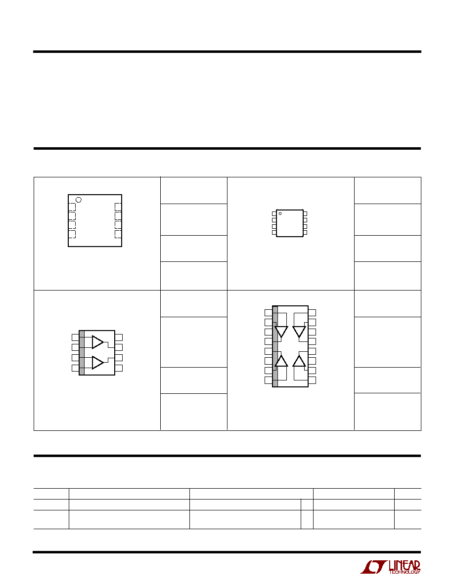
TOP VIEW
V
CC
OUT A
OUT B
GND
+IN A
≠IN A
≠IN B
+IN B
S8 PACKAGE
8-LEAD PLASTIC SO
1
2
3
4
8
7
6
5
T
JMAX
= 150
∞
C,
JA
= 200
∞
C/ W
(Note 1)
Supply Voltage, V
CC
to GND ...................................... 7V
Input Current ......................................................
±
10mA
Output Current (Continuous) .............................
±
20mA
Junction Temperature ........................................... 150
∞
C
(DD Package) ................................................... 125
∞
C
Lead Temperature (Soldering, 10 sec).................. 300
∞
C
1
2
3
4
+IN A
≠IN A
≠IN B
+IN B
8
7
6
5
V
CC
OUT A
OUT B
GND
TOP VIEW
MS8 PACKAGE
8-LEAD PLASTIC MSOP
ORDER PART
NUMBER
1
2
3
4
5
6
7
8
TOP VIEW
GN PACKAGE
16-LEAD NARROW
PLASTIC SSOP
S PACKAGE
16-LEAD PLASTIC SO
16
15
14
13
12
11
10
9
≠IN A
+IN A
GND
OUT A
OUT B
GND
+IN B
≠IN B
≠IN D
+IN D
V
CC
OUT D
OUT C
V
CC
+IN C
≠IN C
LT1720CMS8
LT1720IMS8
MS8
PART MARKING
LTDS
LTACW
T
JMAX
= 150
∞
C,
JA
= 230
∞
C/ W
T
JMAX
= 150
∞
C,
JA
= 135
∞
C/ W (GN)
T
JMAX
= 150
∞
C,
JA
= 115
∞
C/ W (S)
ORDER PART
NUMBER
LT1721CGN
LT1721CS
LT1721IGN
LT1721IS
ORDER PART
NUMBER
LT1720CS8
LT1720IS8
S8
PART MARKING
1720
1720I
Storage Temperature Range ................. ≠ 65
∞
C to 150
∞
C
(DD Package) ................................... ≠ 65
∞
C to 125
∞
C
Operating Temperature Range
C Grade .................................................. 0
∞
C to 70
∞
C
I Grade .............................................. ≠ 40
∞
C to 85
∞
C
GN
PART MARKING
1721
1721I
TOP VIEW
DD PACKAGE
8-LEAD (3mm
◊
3mm) PLASTIC DFN
5
6
7
8
4
3
2
1
+IN A
≠IN A
≠IN B
+IN B
V
CC
OUT A
OUT B
GND
ORDER PART
NUMBER
DD
PART MARKING*
T
JMAX
= 125
∞
C,
JA
= 160
∞
C/ W
UNDERSIDE METAL INTERNALLY
CONNECTED TO GND
SYMBOL
PARAMETER
CONDITIONS
MIN
TYP
MAX
UNITS
V
CC
Supply Voltage
q
2.7
6
V
I
CC
Supply Current (Per Comparator)
V
CC
= 5V
q
4
7
mA
V
CC
= 3V
q
3.5
6
mA
ELECTRICAL CHARACTERISTICS
The
q
denotes specifications that apply over the full operating temperature
range, otherwise specifications are at T
A
= 25
∞
C. V
CC
= 5V, V
CM
= 1V, C
OUT
= 10pF, V
OVERDRIVE
= 20mV, unless otherwise specified.
LT1720CDD
LT1720IDD
LAAV

3
LT1720/LT1721
17201fa
SYMBOL
PARAMETER
CONDITIONS
MIN
TYP
MAX
UNITS
V
CMR
Common Mode Voltage Range
(Note 2)
q
≠ 0.1
V
CC
≠ 1.2
V
V
TRIP
+
Input Trip Points
(Note 3)
≠ 2.0
5.5
mV
q
≠ 3.0
6.5
mV
V
TRIP
≠
Input Trip Points
(Note 3)
≠ 5.5
2.0
mV
q
≠ 6.5
3.0
mV
V
OS
Input Offset Voltage
(Note 3)
1.0
3.0
mV
q
4.5
mV
V
HYST
Input Hysteresis Voltage
(Note 3)
q
2.0
3.5
5.0
mV
V
OS
/
T
Input Offset Voltage Drift
q
10
µ
V/
∞
C
I
B
Input Bias Current
q
≠ 6
0
µ
A
I
OS
Input Offset Current
q
0.6
µ
A
CMRR
Common Mode Rejection Ratio
(Note 4)
q
55
70
dB
PSRR
Power Supply Rejection Ratio
(Note 5)
q
65
80
dB
A
V
Voltage Gain
(Note 6)
V
OH
Output High Voltage
I
SOURCE
= 4mA, V
IN
= V
TRIP
+
+ 10mV
q
V
CC
≠ 0.4
V
V
OL
Output Low Voltage
I
SINK
= 10mA, V
IN
= V
TRIP
≠
≠ 10mV
q
0.4
V
t
PD20
Propagation Delay
V
OVERDRIVE
= 20mV (Note 7)
4.5
6.5
ns
q
8.0
ns
t
PD5
Propagation Delay
V
OVERDRIVE
= 5mV (Notes 7, 8)
7
10
ns
q
13
ns
t
PD
Differential Propagation Delay
(Note 9) Between Channels
0.3
1.0
ns
t
SKEW
Propagation Delay Skew
(Note 10) Between t
PDLH
/t
PDHL
0.5
1.5
ns
t
r
Output Rise Time
10% to 90%
2.5
ns
t
f
Output Fall Time
90% to 10%
2.2
ns
t
JITTER
Output Timing Jitter
V
IN
= 1.2V
P-P
(6dBm), Z
IN
= 50
t
PDLH
15
ps
RMS
V
CM
= 2V, f = 20MHz t
PDHL
11
ps
RMS
f
MAX
Maximum Toggle Frequency
V
OVERDRIVE
= 50mV, V
CC
= 3V
70.0
MHz
V
OVERDRIVE
= 50mV, V
CC
= 5V
62.5
MHz
ELECTRICAL CHARACTERISTICS
The
q
denotes specifications that apply over the full operating temperature
range, otherwise specifications are at T
A
= 25
∞
C. V
CC
= 5V, V
CM
= 1V, C
OUT
= 10pF, V
OVERDRIVE
= 20mV, unless otherwise specified.
Note 1: Absolute Maximum Ratings are those values beyond which the
life of a device may be impaired.
Note 2: If one input is within these common mode limits, the other
input can go outside the common mode limits and the output will be
valid.
Note 3: The LT1720/LT1721 comparators include internal hysteresis.
The trip points are the input voltage needed to change the output state
in each direction. The offset voltage is defined as the average of V
TRIP
+
and V
TRIP
≠
, while the hysteresis voltage is the difference of these two.
Note 4: The common mode rejection ratio is measured with V
CC
= 5V
and is defined as the change in offset voltage measured from V
CM
=
≠ 0.1V to V
CM
= 3.8V, divided by 3.9V.
Note 5: The power supply rejection ratio is measured with V
CM
= 1V
and is defined as the change in offset voltage measured from V
CC
=
2.7V to V
CC
= 6V, divided by 3.3V.
Note 6: Because of internal hysteresis, there is no small-signal region
in which to measure gain. Proper operation of internal circuity is
ensured by measuring V
OH
and V
OL
with only 10mV of overdrive.
Note 7: Propagation delay measurements made with 100mV steps.
Overdrive is measured relative to V
TRIP
±
.
Note 8: t
PD
cannot be measured in automatic handling equipment with
low values of overdrive. The LT1720/LT1721 are 100% tested with a
100mV step and 20mV overdrive. Correlation tests have shown that
t
PD
limits can be guaranteed with this test, if additional DC tests are
performed to guarantee that all internal bias conditions are correct.
Note 9: Differential propagation delay is defined as the larger of the
two:
t
PDLH
= t
PDLH(MAX)
≠ t
PDLH(MIN)
t
PDHL
= t
PDHL(MAX)
≠ t
PDHL(MIN)
where (MAX) and (MIN) denote the maximum and minimum values of
a given measurement across the different comparator channels.
Note 10: Propagation Delay Skew is defined as:
t
SKEW
= |t
PDLH
≠ t
PDHL
|

4
LT1720/LT1721
17201fa
TYPICAL PERFOR
M
A
N
CE CHARACTERISTICS
U
W
SUPPLY VOLTAGE (V)
2.5
V
OS
AND TRIP POINT VOLTAGE (mV)
3
2
1
0
≠1
≠2
≠3
4.0
5.0
1720/21 G01
3.0
3.5
4.5
5.5
6.0
V
TRIP
+
V
OS
V
TRIP
≠
25
∞
C
V
CM
= 1V
Input Offset and Trip Voltages
vs Supply Voltage
TEMPERATURE (
∞
C)
≠ 50
3.6
3.8
4.2
25
75
1720/21 G03
0.2
0
≠ 25
0
50
100
125
≠ 0.2
≠ 0.4
4.0
COMMON MODE INPUT VOLTAGE (V)
V
CC
= 5V
Input Common Mode Limits
vs Temperature
Input Offset and Trip Voltages
vs Temperature
TEMPERATURE (
∞
C)
≠ 3
V
OS
AND TRIP POINT VOLTAGE (mV)
≠ 1
1
3
≠ 2
0
2
≠ 25
25
100
1720/21 G02
≠50
0
50
75
125
V
TRIP
+
V
OS
V
TRIP
≠
Quiescent Supply Current
vs Supply Voltage
Quiescent Supply Current
vs Temperature
Input Current
vs Differential Input Voltage
DIFFERENTIAL INPUT VOLTAGE (V)
≠ 5
≠ 7
INPUT CURRENT (
µ
A)
≠ 6
≠ 4
≠ 3
≠ 2
1
2
3
4
2
1720/21 G04
≠ 5
≠ 4 ≠ 3 ≠ 2 ≠1
0
5
≠1
0
1
25
∞
C
V
CC
= 5V
TEMPERATURE (∞C)
≠ 50
QUIESCENT SUPPLY CURRENT PER COMPARATOR (mA)
5.5
25
1720/21 G05
4.0
3.0
≠ 25
0
50
2.5
2.0
6.0
5.0
4.5
3.5
75
100
125
V
CC
= 5V
V
CC
= 3V
SUPPLY VOLTAGE (V)
0
0
SUPPLY CURRENT PER COMPARATOR (mA)
4
7
2
4
5
1720/21 G06
3
2
1
6
5
1
3
6
7
25
∞
C
125
∞
C
≠ 55
∞
C
Propagation Delay
vs Supply Voltage
Propagation Delay
vs Temperature
Propagation Delay
vs Load Capacitance
OUTPUT LOAD CAPACITANCE (pF)
0
DELAY (ns)
30
50
1720/21 G07
10
20
40
9
8
7
6
5
4
3
2
1
0
25
∞
C
V
STEP
= 100mV
OVERDRIVE = 20mV
V
CC
= 5V
RISING EDGE
(t
PDLH
)
FALLING EDGE
(t
PDHL
)
TEMPERATURE (
∞
C)
≠ 50
PROPAGATION DELAY (ns)
7.5
25
1720/21 G08
6.0
5.0
≠ 25
0
50
4.5
4.0
8.0
7.0
6.5
5.5
75
100
125
V
CC
= 3V
V
CC
= 3V
V
CC
= 5V
V
CC
= 5V
t
PDLH
V
CM
= 1V
V
STEP
= 100mV
C
LOAD
= 10pF
OVERDRIVE = 5mV
OVERDRIVE = 20mV
SUPPLY VOLTAGE (V)
2.5
4.5
DELAY (ns)
5.0
4.0
4.0
5.0
1720/21 G09
3.0
3.5
4.5
5.5
6.0
RISING EDGE
(t
PDLH
)
FALLING EDGE
(t
PDHL
)
25
∞
C
V
STEP
= 100mV
OVERDRIVE = 20mV
C
LOAD
= 10pF

5
LT1720/LT1721
17201fa
TYPICAL PERFOR
M
A
N
CE CHARACTERISTICS
U
W
Output High Voltage
vs Load Current
Output Low Voltage
vs Load Current
OUTPUT SINK CURRENT (mA)
0
OUTPUT VOLTAGE (V)
0.3
0.4
16
1720/21 G10
0.2
0.1
4
8
12
20
0.5
125
∞
C
25
∞
C
125
∞
C
V
CC
= 2.7V
V
CC
= 5V
V
CM
= 1V
V
IN
= ≠ 15mV
≠ 55
∞
C
OUTPUT SOURCE CURRENT (mA)
0
OUTPUT VOLTAGE RELATIVE TO V
CC
(V)
≠ 0.4
≠ 0.2
0.0
16
1720/21 G11
≠ 0.6
≠ 0.8
≠1.0
4
8
12
20
125
∞
C
≠ 55
∞
C
25
∞
C
25
∞
C
V
CC
= 2.7V
V
CC
= 5V
V
CM
= 1V
V
IN
= 15mV
Supply Current vs Frequency
FREQUENCY (MHz)
0
7
8
10
30
NO LOAD
1720/21 G12
6
5
10
20
40
4
3
9
SUPPLY CURRENT PER COMPARATOR (mA)
25
∞
C
V
CC
= 5V
C
LOAD
= 20pF
LT1720
+IN A
(Pin 1): Noninverting Input of Comparator A.
≠IN A (Pin 2): Inverting Input of Comparator A.
≠IN B (Pin 3): Inverting Input of Comparator B.
+IN B (Pin 4): Noninverting Input of Comparator B.
GND (Pin 5): Ground.
OUT B (Pin 6): Output of Comparator B.
OUT A (Pin 7): Output of Comparator A.
V
CC
(Pin 8): Positive Supply Voltage.
PI
N
FU
N
CTIO
N
S
U
U
U
LT1721
≠IN A (Pin 1): Inverting Input of Comparator A.
+IN A
(Pin 2): Noninverting Input of Comparator A.
GND (Pins 3, 6): Ground.
OUT A (Pin 4): Output of Comparator A.
OUT B (Pin 5): Output of Comparator B.
+IN B (Pin 7): Noninverting Input of Comparator B.
≠IN B (Pin 8): Inverting Input of Comparator B.
≠IN C (Pin 9): Inverting Input of Comparator C.
+IN C (Pin 10): Noninverting Input of Comparator C.
V
CC
(Pins 11, 14): Positive Supply Voltage.
OUT C (Pin 12): Output of Comparator C.
OUT D (Pin 13): Output of Comparator D.
+IN D (Pin 15): Noninverting Input of Comparator D.
≠IN D (Pin 16): Inverting Input of Comparator D.