 | ÐлекÑÑоннÑй компоненÑ: LT1812CS8 | СкаÑаÑÑ:  PDF PDF  ZIP ZIP |
Äîêóìåíòàöèÿ è îïèñàíèÿ www.docs.chipfind.ru
1
LT1812
3mA, 100MHz, 750V/
µ
s
Operational Amplifier
with Shutdown
s
100MHz Gain Bandwidth
s
750V/
µ
s Slew Rate
s
3.6mA Maximum Supply Current
s
50
µ
A Supply Current in Shutdown
s
8nV/
Hz Input Noise Voltage
s
Unity-Gain Stable
s
1.5mV Maximum Input Offset Voltage
s
4
µ
A Maximum Input Bias Current
s
400nA Maximum Input Offset Current
s
40mA Minimum Output Current, V
OUT
=
±
3V
s
±
3.5V Minimum Input CMR, V
S
=
±
5V
s
30ns Settling Time to 0.1%, 5V Step
s
Specified at
±
5V, Single 5V Supplies
s
Operating Temperature Range: 40
°
C to 85
°
C
s
Wideband Amplifiers
s
Buffers
s
Active Filters
s
Video and RF Amplification
s
Cable Drivers
s
Data Acquisition Systems
The LT
®
1812 is a low power, high speed, very high slew
rate operational amplifier with excellent DC performance.
The LT1812 features reduced supply current, lower input
offset voltage, lower input bias current and higher DC gain
than other devices with comparable bandwidth. A power
saving shutdown feature reduces supply current to 50
µ
A.
The circuit topology is a voltage feedback amplifier with
the slewing characteristics of a current feedback amplifier.
The output drives a 100
load to
±
3.5V with
±
5V supplies.
On a single 5V supply, the output swings from 1.1V to 3.9V
with a 100
load connected to 2.5V. The amplifier is stable
with a 1000pF capacitive load which makes it useful in
buffer and cable driver applications.
The LT1812 is manufactured on Linear Technology's
advanced low voltage complementary bipolar process.
The dual version is the LT1813. For higher supply voltage
single, dual and quad operational amplifiers with up to
70MHz gain bandwidth, see the LT1351 through LT1365
data sheets.
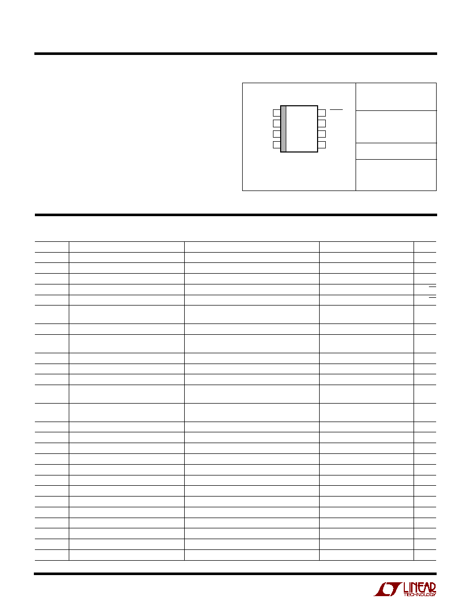
4MHz, 4th Order Butterworth Filter
Filter Frequency Response
FREQUENCY (MHz)
0.1
50
VOLTAGE GAIN (dB)
40
30
20
10
1
10
100
1812 TA02
60
70
80
90
0
10
V
S
=
±
5V
V
IN
= 600mV
P-P
PEAKING < 0.12dB
+
LT1812
220pF
V
IN
665
232
47pF
232
+
LT1812
470pF
1812 TA01
V
OUT
562
274
22pF
274
, LTC and LT are registered trademarks of Linear Technology Corporation.
FEATURES
APPLICATIO S
U
TYPICAL APPLICATIO
U
DESCRIPTIO
U
2
LT1812
(Note 1)
Total Supply Voltage (V
+
to V
) ............................. 12.6V
Differential Input Voltage (Transient Only, Note 2) ...
±
3V
Input Voltage ...........................................................
±
V
S
Output Short-Circuit Duration (Note 3) ............ Indefinite
Operating Temperature Range (Note 8) ... 40
°
C to 85
°
C
Specified Temperature Range
(Note 8) .............................................. 40
°
C to 85
°
C
Maximum Junction Temperature ......................... 150
°
C
Storage Temperature Range .................. 65
°
C to 150
°
C
Lead Temperature (Soldering, 10 sec)................... 300
°
C
Consult factory for Military grade parts.
T
JMAX
= 150
°
C,
JA
= 80
°
C/ W (NOTE 9)
ORDER PART
NUMBER
LT1812CS8
LT1812IS8
S8 PART MARKING
1812
1812I
SYMBOL
PARAMETER
CONDITIONS
MIN
TYP
MAX
UNITS
V
OS
Input Offset Voltage
(Note 4)
0.4
1.5
mV
I
OS
Input Offset Current
30
400
nA
I
B
Input Bias Current
0.9
±
4
µ
A
e
n
Input Noise Voltage Density
f = 10kHz
8
nV/
Hz
i
n
Input Noise Current Density
f = 10kHz
1
pA/
Hz
R
IN
Input Resistance
V
CM
=
±
3.5V
3
10
M
Differential
1.5
M
C
IN
Input Capacitance
2
pF
V
CM
Input Voltage Range (Positive)
3.5
4.2
V
Input Voltage Range (Negative)
4.2
3.5
V
CMRR
Common Mode Rejection Ratio
V
CM
=
±
3.5V
75
85
dB
Minimum Supply Voltage
±
1.25
±
2
V
PSRR
Power Supply Rejection Ratio
V
S
=
±
2V to
±
5.5V
78
97
dB
A
VOL
Large-Signal Voltage Gain
V
OUT
=
±
3V, R
L
= 500
1.5
3.0
V/mV
V
OUT
=
±
3V, R
L
= 100
1.0
2.5
V/mV
V
OUT
Maximum Output Swing
R
L
= 500
, 30mV Overdrive
±
3.80
±
4.0
V
R
L
= 100
, 30mV Overdrive
±
3.35
±
3.5
V
I
OUT
Maximum Output Current
V
OUT
=
±
3V, 30mV Overdrive
±
40
±
60
mA
I
SC
Output Short-Circuit Current
V
OUT
= 0V, 1V Overdrive (Note 3)
±
75
±
110
mA
SR
Slew Rate
A
V
= 1 (Note 5)
500
750
V/
µ
s
FPBW
Full Power Bandwidth
3V Peak (Note 6)
40
MHz
GBW
Gain Bandwidth Product
f = 200kHz
75
100
MHz
t
r
, t
f
Rise Time, Fall Time
A
V
= 1, 10% to 90%, 0.1V, R
L
= 100
2
ns
OS
Overshoot
A
V
= 1, 0.1V, R
L
= 100
25
%
t
PD
Propagation Delay
A
V
= 1, 50% V
IN
to 50% V
OUT
, 0.1V, R
L
= 100
2.8
ns
t
s
Settling Time
5V Step, 0.1%, A
V
= 1
30
ns
THD
Total Harmonic Distortion
f = 1MHz, V
OUT
= 2V
P-P
, A
V
= 2, R
L
= 500
76
dB
Differential Gain
V
OUT
= 2V
P-P
, A
V
= 2, R
L
= 150
0.12
%
Differential Phase
V
OUT
= 2V
P-P
, A
V
= 2, R
L
= 150
0.07
DEG
R
OUT
Output Resistance
A
V
= 1, f = 1MHz
0.4
T
A
= 25
°
C, V
S
=
±
5V, V
CM
= 0V unless otherwise noted.
1
2
3
4
8
7
6
5
TOP VIEW
SHDN
V
+
V
OUT
NC
NC
IN
+IN
V
S8 PACKAGE
8-LEAD PLASTIC SO
ABSOLUTE AXI U RATI GS
W
W
W
U
PACKAGE/ORDER I FOR ATIO
U
U
W
ELECTRICAL CHARACTERISTICS
3
LT1812
SYMBOL
PARAMETER
CONDITIONS
MIN
TYP
MAX
UNITS
V
OS
Input Offset Voltage
(Note 4)
0.5
2.0
mV
I
OS
Input Offset Current
30
400
nA
I
B
Input Bias Current
1.0
±
4
µ
A
e
n
Input Noise Voltage Density
f = 10kHz
8
nV/
Hz
i
n
Input Noise Current Density
f = 10kHz
1
pA/
Hz
R
IN
Input Resistance
V
CM
= 1.5V to 3.5V
3
10
M
Differential
1.5
M
C
IN
Input Capacitance
2
pF
V
CM
Input Voltage Range (Positive)
3.5
4
V
Input Voltage Range (Negative)
1
1.5
V
CMRR
Common Mode Rejection Ratio
V
CM
= 1.5V to 3.5V
73
82
dB
A
VOL
Large-Signal Voltage Gain
V
OUT
= 1.5V to 3.5V, R
L
= 500
1.0
2.0
V/mV
V
OUT
= 1.5V to 3.5V, R
L
= 100
0.7
1.5
V/mV
V
OUT
Maximum Output Swing (Positive)
R
L
= 500
, 30mV Overdrive
3.9
4.1
V
R
L
= 100
, 30mV Overdrive
3.7
3.9
V
Maximum Output Swing (Negative)
R
L
= 500
, 30mV Overdrive
0.9
1.1
V
R
L
= 100
, 30mV Overdrive
1.1
1.3
V
I
OUT
Maximum Output Current
V
OUT
= 3.5V or 1.5V, 30mV Overdrive
±
25
±
40
mA
I
SC
Output Short-Circuit Current
V
OUT
= 2.5V, 1V Overdrive (Note 3)
±
55
±
80
mA
SR
Slew Rate
A
V
= 1 (Note 5)
200
350
V/
µ
s
FPBW
Full Power Bandwidth
1V Peak (Note 6)
55
MHz
GBW
Gain Bandwidth Product
f = 200kHz
65
94
MHz
t
r
, t
f
Rise Time, Fall Time
A
V
= 1, 10% to 90%, 0.1V, R
L
= 100
2.1
ns
OS
Overshoot
A
V
= 1, 0.1V, R
L
= 100
25
%
t
PD
Propagation Delay
A
V
= 1, 50% V
IN
to 50% V
OUT
, 0.1V, R
L
= 100
3
ns
t
s
Settling Time
2V Step, 0.1%, A
V
= 1
30
ns
THD
Total Harmonic Distortion
f = 1MHz, V
OUT
= 2V
P-P
, A
V
= 2, R
L
= 500
75
dB
Differential Gain
V
OUT
= 2V
P-P
, A
V
= 2, R
L
= 150
0.22
%
Differential Phase
V
OUT
= 2V
P-P
, A
V
= 2, R
L
= 150
0.21
DEG
R
OUT
Output Resistance
A
V
= 1, f = 1MHz
0.45
I
SHDN
SHDN Pin Current
SHDN > V
+ 2.0V (On)
0
±
1
µ
A
SHDN < V
+ 0.4V (Off)
50
20
µ
A
I
S
Supply Current
SHDN > V
+ 2.0V (On)
2.7
3.6
mA
SHDN < V
+ 0.4V (Off)
20
50
µ
A
T
A
= 25
°
C, V
S
= 5V, V
CM
= 2.5V, R
L
to 2.5V unless otherwise noted.
SYMBOL
PARAMETER
CONDITIONS
MIN
TYP
MAX
UNITS
I
SHDN
SHDN Pin Current
SHDN > V
+ 2.0V (On)
0
±
1
µ
A
SHDN < V
+ 0.4V (Off)
100
50
µ
A
I
S
Supply Current
SHDN > V
+ 2.0V (On)
3
3.6
mA
SHDN < V
+ 0.4V (Off)
50
100
µ
A
T
A
= 25
°
C, V
S
=
±
5V, V
CM
= 0V unless otherwise noted.
ELECTRICAL CHARACTERISTICS
SYMBOL
PARAMETER
CONDITIONS
MIN
TYP
MAX
UNITS
V
OS
Input Offset Voltage
(Note 4)
2
mV
V
OS
/
T
Input Offset Voltage Drift
(Note 7)
10
15
µ
V/
°
C
I
OS
Input Offset Current
500
nA
I
B
Input Bias Current
±
5
µ
A
0
°
C
T
A
70
°
C, V
S
=
±
5V, V
CM
= 0V unless otherwise noted.
4
LT1812
0
°
C
T
A
70
°
C. V
S
=
±
5V, V
CM
= 0V unless otherwise noted.
ELECTRICAL CHARACTERISTICS
SYMBOL
PARAMETER
CONDITIONS
MIN
TYP
MAX
UNITS
V
CM
Input Voltage Range (Positive)
3.5
V
Input Voltage Range (Negative)
3.5
V
CMRR
Common Mode Rejection Ratio
V
CM
=
±
3.5V
73
dB
Minimum Supply Voltage
±
2
V
PSRR
Power Supply Rejection Ratio
V
S
=
±
2V to
±
5.5V
76
dB
A
VOL
Large-Signal Voltage Gain
V
OUT
=
±
3V, R
L
= 500
1.0
V/mV
V
OUT
=
±
3V, R
L
= 100
0.7
V/mV
V
OUT
Maximum Output Swing
R
L
= 500
, 30mV Overdrive
±
3.70
V
R
L
= 100
, 30mV Overdrive
±
3.25
V
I
OUT
Maximum Output Current
V
OUT
=
±
3V, 30mV Overdrive
±
35
mA
I
SC
Output Short-Circuit Current
V
OUT
= 0V, 1V Overdrive (Note 3)
±
60
mA
SR
Slew Rate
A
V
= 1 (Note 5)
400
V/
µ
s
GBW
Gain Bandwidth Product
f = 200kHz
65
MHz
I
SHDN
SHDN Pin Current
SHDN > V
+ 2.0V (On)
±
1.5
µ
A
SHDN < V
+ 0.4V (Off)
150
µ
A
I
S
Supply Current
SHDN > V
+ 2.0V (On)
4.6
mA
SHDN < V
+ 0.4V (Off)
150
µ
A
0
°
C
T
A
70
°
C, V
S
= 5V, V
CM
= 2.5V, R
L
to 2.5V unless otherwise noted.
V
OS
Input Offset Voltage
(Note 4)
2.5
mV
V
OS
/
T
Input Offset Voltage Drift
(Note 7)
10
15
µ
V/
°
C
I
OS
Input Offset Current
500
nA
I
B
Input Bias Current
±
5
µ
A
V
CM
Input Voltage Range (Positive)
3.5
V
Input Voltage Range (Negative)
1.5
V
CMRR
Common Mode Rejection Ratio
V
CM
= 1.5V to 3.5V
71
dB
A
VOL
Large-Signal Voltage Gain
V
OUT
= 1.5V to 3.5V, R
L
= 500
0.7
V/mV
V
OUT
= 1.5V to 3.5V, R
L
= 100
0.5
V/mV
V
OUT
Maximum Output Swing (Positive)
R
L
= 500
, 30mV Overdrive
3.8
V
R
L
= 100
, 30mV Overdrive
3.6
V
Maximum Output Swing (Negative)
R
L
= 500
, 30mV Overdrive
1.2
V
R
L
= 100
, 30mV Overdrive
1.4
V
I
OUT
Maximum Output Current
V
OUT
= 3.5V or 1.5V, 30mV Overdrive
±
20
mA
I
SC
Output Short-Circuit Current
V
OUT
= 2.5V, 1V Overdrive (Note 3)
±
45
mA
SR
Slew Rate
A
V
= 1 (Note 5)
150
V/
µ
s
GBW
Gain Bandwidth Product
f = 200kHz
55
MHz
I
SHDN
SHDN Pin Current
SHDN > V
+ 2.0V (On)
±
1.5
µ
A
SHDN < V
+ 0.4V (Off)
75
µ
A
I
S
Supply Current
SHDN > V
+ 2.0V (On)
4.5
mA
SHDN < V
+ 0.4V (Off)
75
µ
A
40
°
C
T
A
85
°
C. V
S
=
±
5V, V
CM
= 0V unless otherwise noted (Note 8).
SYMBOL
PARAMETER
CONDITIONS
MIN
TYP
MAX
UNITS
V
OS
Input Offset Voltage
(Note 4)
3
mV
V
OS
/
T
Input Offset Voltage Drift
(Note 7)
10
30
µ
V/
°
C
I
OS
Input Offset Current
600
nA
I
B
Input Bias Current
±
6
µ
A
V
CM
Input Voltage Range (Positive)
3.5
V
Input Voltage Range (Negative)
3.5
V
CMRR
Common Mode Rejection Ratio
V
CM
=
±
3.5V
72
dB
5
LT1812
SYMBOL
PARAMETER
CONDITIONS
MIN
TYP
MAX
UNITS
Minimum Supply Voltage
±
2
V
PSRR
Power Supply Rejection Ratio
V
S
=
±
2V to
±
5.5V
75
dB
A
VOL
Large-Signal Voltage Gain
V
OUT
=
±
3V, R
L
= 500
0.8
V/mV
V
OUT
=
±
3V, R
L
= 100
0.6
V/mV
V
OUT
Maximum Output Swing
R
L
= 500
, 30mV Overdrive
±
3.60
V
R
L
= 100
, 30mV Overdrive
±
3.15
V
I
OUT
Maximum Output Current
V
OUT
=
±
3V, 30mV Overdrive
±
30
mA
I
SC
Output Short-Circuit Current
V
OUT
= 0V, 1V Overdrive (Note 3)
±
55
mA
SR
Slew Rate
A
V
= 1 (Note 5)
350
V/
µ
s
GBW
Gain Bandwidth Product
f = 200kHz
60
MHz
I
SHDN
SHDN Pin Current
SHDN > V
+ 2.0V (On)
±
2
µ
A
SHDN < V
+ 0.4V (Off)
200
µ
A
I
S
Supply Current
SHDN > V
+ 2.0V (On)
5
mA
SHDN < V
+ 0.4V (Off)
200
µ
A
ELECTRICAL CHARACTERISTICS
Note 1: Absolute Maximum Ratings are those values beyond which the life of
the device may be impaired.
Note 2: Differential inputs of
±
3V are appropriate for transient operation only,
such as during slewing. Large sustained differential inputs can cause
excessive power dissipation and may damage the part.
Note 3: A heat sink may be required to keep the junction temperature below
absolute maximum when the output is shorted indefinitely.
Note 4: Input offset voltage is pulse tested and is exclusive of warm-up drift.
Note 5: Slew rate is measured between
±
2V on the output with
±
3V input for
±
5V supplies and 2V
P-P
on the output with a 3V
P-P
input for single 5V
supplies.
Note 6: Full power bandwidth is calculated from the slew rate:
FPBW = SR/2
V
P
.
Note 7: This parameter is not 100% tested.
Note 8: The LT1812C is guaranteed to meet specified performance from
0
°
C to 70
°
C. The LT1812C is designed, characterized and expected to meet
specified performance from 40
°
C to 85
°
C but is not tested or QA sampled
at these temperatures. The LT1812I is guaranteed to meet specified
performance from 40
°
C to 85
°
C.
Note 9:
JA
is specified for a 2500mm
2
board covered with 2 oz copper on
both sides. Thermal resistance varies, depending upon the amount of PC
board metal attached to the device. For this package in particular, power is
dissipated primarily through Pin 4, which should therefore, have a good
thermal connection to a copper plane.
40
°
C
T
A
85
°
C. V
S
=
±
5V, V
CM
= 0V unless otherwise noted (Note 8).
40
°
C
T
A
85
°
C, V
S
= 5V, V
CM
= 2.5V, R
L
to 2.5V unless otherwise noted (Note 8).
SYMBOL
PARAMETER
CONDITIONS
MIN
TYP
MAX
UNITS
V
OS
Input Offset Voltage
(Note 4)
3.5
mV
V
OS
/
T
Input Offset Voltage Drift
(Note 7)
10
30
µ
V/
°
C
I
OS
Input Offset Current
600
nA
I
B
Input Bias Current
±
6
µ
A
V
CM
Input Voltage Range (Positive)
3.5
V
Input Voltage Range (Negative)
1.5
V
CMRR
Common Mode Rejection Ratio
V
CM
= 1.5V to 3.5V
70
dB
A
VOL
Large-Signal Voltage Gain
V
OUT
= 1.5V to 3.5V, R
L
= 500
0.6
V/mV
V
OUT
= 2.0V to 3.0V, R
L
= 100
0.4
V/mV
V
OUT
Maximum Output Swing (Positive)
R
L
= 500
, 30mV Overdrive
3.7
V
R
L
= 100
, 30mV Overdrive
3.5
V
Maximum Output Swing (Negative)
R
L
= 500
, 30mV Overdrive
1.3
V
R
L
= 100
, 30mV Overdrive
1.5
V
I
OUT
Maximum Output Current
V
OUT
= 3.5V or 1.5V, 30mV Overdrive
±
17
mA
I
SC
Output Short-Circuit Current
V
OUT
= 2.5V, 1V Overdrive (Note 3)
±
40
mA
SR
Slew Rate
A
V
= 1 (Note 5)
125
V/
µ
s
GBW
Gain Bandwidth Product
f = 200kHz
50
MHz
I
SHDN
SHDN Pin Current
SHDN > V
+ 2.0V (On)
±
2
µ
A
SHDN < V
+ 0.4V (Off)
100
µ
A
I
S
Supply Current
SHDN > V
+ 2.0V (On)
5
mA
SHDN < V
+ 0.4V (Off)
100
µ
A