1
LT1818/LT1819
18189f
400MHz, 2500V/
µ
s, 9mA
Single/Dual Operational Amplifiers
s
400MHz Gain Bandwidth Product
s
2500V/
µ
s Slew Rate
s
≠85dBc Distortion at 5MHz
s
9mA Supply Current Per Amplifier
s
Space Saving SOT-23 and MS8 Packages
s
6nV/
Hz Input Noise Voltage
s
Unity-Gain Stable
s
1.5mV Maximum Input Offset Voltage
s
8
µ
A Maximum Input Bias Current
s
800nA Maximum Input Offset Current
s
40mA Minimum Output Current, V
OUT
=
±
3V
s
±
3.5V Minimum Input CMR, V
S
=
±
5V
s
Specified at
±
5V, Single 5V Supplies
s
Operating Temperature Range: ≠ 40
∞
C to 85
∞
C
s
Wideband Amplifiers
s
Buffers
s
Active Filters
s
Video and RF Amplification
s
Communication Receivers
s
Cable Drivers
s
Data Acquisition Systems
, LTC and LT are registered trademarks of Linear Technology Corporation.
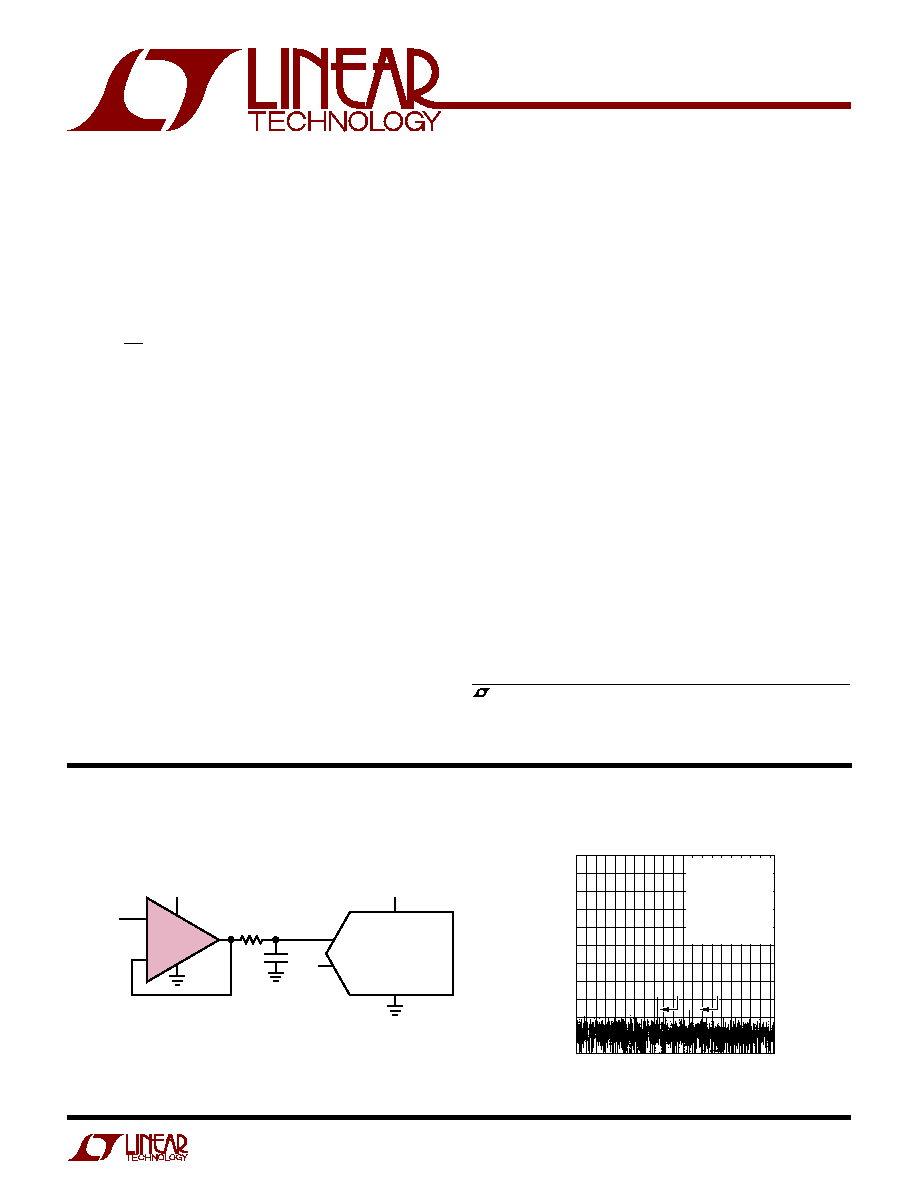
The LT
Æ
1818/LT1819 are single/dual wide bandwidth,
high slew rate, low noise and distortion operational ampli-
fiers with excellent DC performance. The LT1818/LT1819
have been designed for wider bandwidth and slew rate,
much lower input offset voltage and lower noise and
distortion than devices with comparable supply current.
The circuit topology is a voltage feedback amplifier with
the excellent slewing characteristics of a current feedback
amplifier.
The output drives a 100
load to
±
3.8V with
±
5V supplies.
On a single 5V supply, the output swings from 1V to 4V
with a 100
load connected to 2.5V. The amplifier is unity-
gain stable with a 20pF capacitive load without the need for
a series resistor. Harmonic distortion is ≠85dBc up to
5MHz for a 2V
P-P
output at a gain of 2.
The LT1818/LT1819 are manufactured on Linear
Technology's advanced low voltage complementary bipo-
lar process. The LT1818 (single op amp) is available in
SOT-23 and SO-8 packages; the LT1819 (dual op amp) is
available in MSOP-8 and SO-8 packages.
≠
+
LT1818
2.5VDC
±
1VAC
18189 TA01
18pF
2.5V
51.1
5V
5V
A
IN
+
LTC1744
14 BITS
50Msps
(SET FOR 2V
P-P
FULL SCALE)
A
IN
≠
Single Supply Unity-Gain ADC Driver for Oversampling Applications
FREQUENCY (Hz)
AMPLITUDE (dBc)
0
≠10
≠20
≠30
≠40
≠50
≠60
≠70
≠80
≠90
≠100
≠110
0
18189 TA02
5M
10M
15M
20M
25M
f
IN
= 5.102539MHz
f
S
= 50Msps
V
IN
= 300mV
P-P
SFDR = 78dB
8192 POINT FFT
NO WINDOWING
OR AVERAGING
2
3
FFT of Single Supply ADC Driver
APPLICATIO S
U
FEATURES
TYPICAL APPLICATIO
U
DESCRIPTIO
U

2
LT1818/LT1819
18189f
(Note 1)
Total Supply Voltage (V
+
to V
≠
) ........................... 12.6V
Differential Input Voltage
(Transient Only, Note 2) .....................................
±
6V
Output Short-Circuit Duration (Note 3) ........... Indefinite
Operating Temperature Range (Note 8) .. ≠ 40
∞
C to 85
∞
C
ABSOLUTE AXI U RATI GS
W
W
W
U
PACKAGE/ORDER I FOR ATIO
U
U
W
*The temperature grade is identified by a label on the shipping container. Consult LTC Marketing for parts specified with wider operating temperature ranges.
Specified Temperature Range (Note 9) ... ≠40
∞
C to 85
∞
C
Maximum Junction Temperature .......................... 150
∞
C
Storage Temperature Range ................. ≠ 65
∞
C to 150
∞
C
Lead Temperature (Soldering, 10 sec).................. 300
∞
C
1
2
3
4
OUT A
≠IN A
+IN A
V
≠
8
7
6
5
V
+
OUT B
≠IN B
+IN B
TOP VIEW
MS8 PACKAGE
8-LEAD PLASTIC MSOP
B
A
TOP VIEW
S5 PACKAGE
5-LEAD PLASTIC SOT-23
1
2
3
OUT 1
V
≠
+IN
5
4
V+
≠IN
+
≠
LTF7
S5 PART*
MARKING
ORDER PART
NUMBER
LT1818CS5
LT1818IS5
LTE7
LTE5
MS8 PART
MARKING
ORDER PART
NUMBER
T
JMAX
= 150
∞
C,
JA
= 250
∞
C/W (NOTE 10)
T
JMAX
= 150
∞
C,
JA
= 250
∞
C/W (NOTE 10)
LT1819CMS8
LT1819IMS8
T
JMAX
= 150
∞
C,
JA
= 150
∞
C/W (NOTE 10)
1
2
3
4
8
7
6
5
TOP VIEW
≠
+
NC
V
+
OUT
NC
NC
≠IN
+IN
V
≠
S8 PACKAGE
8-LEAD PLASTIC SO
LT1818CS8
LT1818IS8
ORDER PART
NUMBER
1818
1818I
S8 PART
MARKING
T
JMAX
= 150
∞
C,
JA
= 150
∞
C/W (NOTE 10)
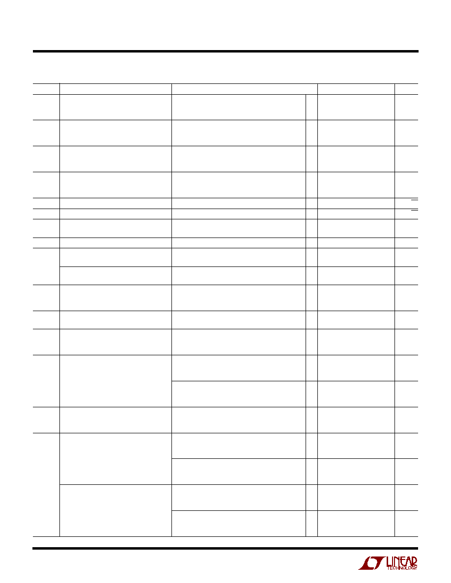
ELECTRICAL CHARACTERISTICS
SYMBOL
PARAMETER
CONDITIONS
MIN
TYP
MAX
UNITS
V
OS
Input Offset Voltage
(Note 4)
0.2
1.5
mV
T
A
= 0
∞
C to 70
∞
C
q
2.0
mV
T
A
= ≠40
∞
C to 85
∞
C
q
3.0
mV
V
OS
/
T
Input Offset Voltage Drift
T
A
= 0
∞
C to 70
∞
C (Note 7)
q
10
15
µ
V/
∞
C
T
A
= ≠40
∞
C to 85
∞
C (Note 7)
q
10
30
µ
V/
∞
C
I
OS
Input Offset Current
60
800
nA
T
A
= 0
∞
C to 70
∞
C
q
1000
nA
T
A
= ≠40
∞
C to 85
∞
C
q
1200
nA
I
B
Input Bias Current
≠2
±
8
µ
A
T
A
= 0
∞
C to 70
∞
C
q
±
10
µ
A
T
A
= ≠40
∞
C to 85
∞
C
q
±
12
µ
A
e
n
Input Noise Voltage Density
f = 10kHz
6
nV/
Hz
i
n
Input Noise Current Density
f = 10kHz
1.2
pA/
Hz
The
q
denotes the specifications which apply over the full operating
temperature range, otherwise specifications are at T
A
= 25
∞
C. (Note 9) V
S
=
±
5V, V
CM
= 0V, unless otherwise noted.
LT1819CS8
LT1819IS8
ORDER PART
NUMBER
1819
1819I
S8 PART
MARKING
1
2
3
4
8
7
6
5
TOP VIEW
V
+
OUT B
≠IN B
+IN B
OUT A
≠IN A
+IN A
V
≠
S8 PACKAGE
8-LEAD PLASTIC SO
A
B

3
LT1818/LT1819
18189f
SYMBOL
PARAMETER
CONDITIONS
MIN
TYP
MAX
UNITS
R
IN
Input Resistance
V
CM
= V
≠
+ 1.5V to V
+
≠ 1.5V
1.5
5
M
Differential
750
k
C
IN
Input Capacitance
1.5
pF
V
CM
Input Voltage Range
Guaranteed by CMRR
±
3.5
±
4.2
V
(Positive/Negative)
T
A
= ≠40
∞
C to 85
∞
C
q
±
3.5
V
CMRR
Common Mode Rejection Ratio
V
CM
=
±
3.5V
75
85
dB
T
A
= 0
∞
C to 70
∞
C
q
73
dB
T
A
= ≠40
∞
C to 85
∞
C
q
72
dB
Minimum Supply Voltage
Guaranteed by PSRR
±
1.25
±
2
V
T
A
= ≠40
∞
C to 85
∞
C
q
±
2
V
PSRR
Power Supply Rejection Ratio
V
S
=
±
2V to
±
5.5V
78
97
dB
T
A
= 0
∞
C to 70
∞
C
q
76
dB
T
A
= ≠40
∞
C to 85
∞
C
q
75
dB
A
VOL
Large-Signal Voltage Gain
V
OUT
=
±
3V, R
L
= 500
1.5
2.5
V/mV
T
A
= 0
∞
C to 70
∞
C
q
1.0
V/mV
T
A
= ≠40
∞
C to 85
∞
C
q
0.8
V/mV
V
OUT
=
±
3V, R
L
= 100
1.0
6
V/mV
T
A
= 0
∞
C to 70
∞
C
q
0.7
V/mV
T
A
= ≠40
∞
C to 85
∞
C
q
0.6
V/mV
Channel Separation
V
OUT
=
±
3V, LT1819
82
100
dB
T
A
= 0
∞
C to 70
∞
C
q
81
dB
T
A
= ≠40
∞
C to 85
∞
C
q
80
dB
V
OUT
Output Swing(Positive/Negative)
R
L
= 500
, 30mV Overdrive
±
3.8
±
4.1
V
T
A
= 0
∞
C to 70
∞
C
q
±
3.7
V
T
A
= ≠40
∞
C to 85
∞
C
q
±
3.6
V
R
L
= 100
, 30mV Overdrive
±
3.50
±
3.8
V
T
A
= 0
∞
C to 70
∞
C
q
±
3.25
V
T
A
= ≠40
∞
C to 85
∞
C
q
±
3.15
V
I
OUT
Output Current
V
OUT
=
±
3V, 30mV Overdrive
±
40
±
70
mA
T
A
= 0
∞
C to 70
∞
C
q
±
35
mA
T
A
= ≠40
∞
C to 85
∞
C
q
±
30
mA
I
SC
Output Short-Circuit Current
V
OUT
= 0V, 1V Overdrive (Note 3)
±
100
±
200
mA
T
A
= 0
∞
C to 70
∞
C
q
±
90
mA
T
A
= ≠40
∞
C to 85
∞
C
q
±
70
mA
SR
Slew Rate
A
V
= 1
2500
V/
µ
s
A
V
= ≠1 (Note 5)
900
1800
V/
µ
s
T
A
= 0
∞
C to 70
∞
C
q
750
V/
µ
s
T
A
= ≠40
∞
C to 85
∞
C
q
600
V/
µ
s
FPBW
Full Power Bandwidth
6V
P-P
(Note 6)
95
MHz
GBW
Gain Bandwidth Product
f = 4MHz, R
L
= 500
270
400
MHz
T
A
= 0
∞
C to 70
∞
C
q
260
MHz
T
A
= ≠40
∞
C to 85
∞
C
q
250
MHz
t
r
, t
f
Rise Time, Fall Time
A
V
= 1, 10% to 90%, 0.1V Step
0.6
ns
t
PD
Propagation Delay
A
V
= 1, 50% to 50%, 0.1V Step
1.0
ns
OS
Overshoot
A
V
= 1, 0.1V, R
L
= 100
20
%
t
S
Settling Time
A
V
= ≠1, 0.1%, 5V
10
ns
HD
Harmonic Distortion
HD2, A
V
= 2, f = 5MHz, V
OUT
= 2V
P-P
, R
L
= 500
≠85
dBc
HD3, A
V
= 2, f = 5MHz, V
OUT
= 2V
P-P
, R
L
= 500
≠89
dBc
dG
Differential Gain
A
V
= 2, R
L
= 150
0.07
%
dP
Differential Phase
A
V
= 2, R
L
= 150
0.02
DEG
I
S
Supply Current
Per Amplifier
9
10
mA
T
A
= 0
∞
C to 70
∞
C
q
13
mA
T
A
= ≠40
∞
C to 85
∞
C
q
14
mA
ELECTRICAL CHARACTERISTICS
The
q
denotes the specifications which apply over the full operating
temperature range, otherwise specifications are at T
A
= 25
∞
C. (Note 9) V
S
=
±
5V, V
CM
= 0V, unless otherwise noted.
4
LT1818/LT1819
18189f
ELECTRICAL CHARACTERISTICS
The
q
denotes the specifications which apply over the full operating
temperature range, otherwise specifications are at T
A
= 25
∞
C (Note 9). V
S
= 5V, 0V; V
CM
= 2.5V, R
L
to 2.5V unless otherwise noted.
SYMBOL
PARAMETER
CONDITIONS
MIN
TYP
MAX
UNITS
V
OS
Input Offset Voltage
(Note 4)
0.4
2.0
mV
T
A
= 0
∞
C to 70
∞
C
q
2.5
mV
T
A
= ≠40
∞
C to 85
∞
C
q
3.5
mV
V
OS
/
T
Input Offset Voltage Drift
(Note 7)
T
A
= 0
∞
C to 70
∞
C
q
10
15
µ
V/
∞
C
T
A
= ≠40
∞
C to 85
∞
C
q
10
30
µ
V/
∞
C
I
OS
Input Offset Current
60
800
nA
T
A
= 0
∞
C to 70
∞
C
q
1000
nA
T
A
= ≠40
∞
C to 85
∞
C
q
1200
nA
I
B
Input Bias Current
≠2.4
±
8
µ
A
T
A
= 0
∞
C to 70
∞
C
q
±
10
µ
A
T
A
= ≠40
∞
C to 85
∞
C
q
±
12
µ
A
e
n
Input Noise Voltage Density
f = 10kHz
6
nV/
Hz
i
n
Input Noise Current Density
f = 10kHz
1.4
pA/
Hz
R
IN
Input Resistance
V
CM
= V
≠
+ 1.5V to V
+
≠ 1.5V
1.5
5
M
Differential
750
k
C
IN
Input Capacitance
1.5
pF
V
CM
Input Voltage Range (Positive)
Guaranteed by CMRR
3.5
4.2
V
T
A
= ≠40
∞
C to 85
∞
C
q
3.5
V
Input Voltage Range (Negative)
Guaranteed by CMRR
0.8
1.5
V
T
A
= ≠40
∞
C to 85
∞
C
q
1.5
V
CMRR
Common Mode Rejection Ratio
V
CM
= 1.5V to 3.5V
73
82
dB
T
A
= 0
∞
C to 70
∞
C
q
71
dB
T
A
= ≠40
∞
C to 85
∞
C
q
70
dB
Minimum Supply Voltage
Guaranteed by PSRR
±
1.25
±
2
V
T
A
= ≠40
∞
C to 85
∞
C
q
±
2
V
PSRR
Power Supply Rejection Ratio
V
S
= 4V to 11V
78
97
dB
T
A
= 0
∞
C to 70
∞
C
q
76
dB
T
A
= ≠40
∞
C to 85
∞
C
q
75
dB
A
VOL
Large-Signal Voltage Gain
V
OUT
= 1.5V to 3.5V, R
L
= 500
1.0
2
V/mV
T
A
= 0
∞
C to 70
∞
C
q
0.7
V/mV
T
A
= ≠40
∞
C to 85
∞
C
q
0.6
V/mV
V
OUT
= 1.5V to 3.5V, R
L
= 100
0.7
4
V/mV
T
A
= 0
∞
C to 70
∞
C
q
0.5
V/mV
T
A
= ≠40
∞
C to 85
∞
C
q
0.4
V/mV
Channel Separation
V
OUT
= 1.5V to 3.5V, LT1819
81
100
dB
T
A
= 0
∞
C to 70
∞
C
q
80
dB
T
A
= ≠40
∞
C to 85
∞
C
q
79
dB
V
OUT
Output Swing(Positive)
R
L
= 500
, 30mV Overdrive
3.9
4.2
V
T
A
= 0
∞
C to 70
∞
C
q
3.8
V
T
A
= ≠40
∞
C to 85
∞
C
q
3.7
V
R
L
= 100
, 30mV Overdrive
3.7
4
V
T
A
= 0
∞
C to 70
∞
C
q
3.6
V
T
A
= ≠40
∞
C to 85
∞
C
q
3.5
V
Output Swing(Negative)
R
L
= 500
, 30mV Overdrive
0.8
1.1
V
T
A
= 0
∞
C to 70
∞
C
q
1.2
V
T
A
= ≠40
∞
C to 85
∞
C
q
1.3
V
R
L
= 100
, 30mV Overdrive
1
1.3
V
T
A
= 0
∞
C to 70
∞
C
q
1.4
V
T
A
= ≠40
∞
C to 85
∞
C
q
1.5
V

5
LT1818/LT1819
18189f
ELECTRICAL CHARACTERISTICS
The
q
denotes the specifications which apply over the full operating
temperature range, otherwise specifications are at T
A
= 25
∞
C (Note 9). V
S
= 5V, 0V; V
CM
= 2.5V, R
L
to 2.5V unless otherwise noted.
Note 1: Absolute Maximum Ratings are those values beyond which the life
of a device may be impaired.
Note 2: Differential inputs of
±
6V are appropriate for transient operation
only, such as during slewing. Large sustained differential inputs can cause
excessive power dissipation and may damage the part.
Note 3: A heat sink may be required to keep the junction temperature
below absolute maximum when the output is shorted indefinitely.
Note 4: Input offset voltage is pulse tested and is exclusive of warm-up
drift.
Note 5: With
±
5V supplies, slew rate is tested in a closed-loop gain of ≠1
by measuring the rise time of the output from ≠2V to 2V with an output
step from ≠3V to 3V. With single 5V supplies, slew rate is tested in a
closed-loop gain of ≠1 by measuring the rise time of the output from 1.5V
to 3.5V with an output step from 1V to 4V. Falling edge slew rate is not
production tested, but is designed, characterized and expected to be within
10% of the rising edge slew rate.
Note 6: Full power bandwidth is calculated from the slew rate:
FPBW = SR/2
V
P
Note 7: This parameter is not 100% tested.
Note 8: The LT1818C/LT1818I and LT1819C/LT1819I are guaranteed
functional over the operating temperature range of ≠ 40
∞
C to 85
∞
C.
Note 9: The LT1818C/LT1819C are guaranteed to meet specified
performance from 0
∞
C to 70
∞
C and is designed, characterized and
expected to meet the extended temperature limits, but is not tested at
≠40
∞
C and 85
∞
C. The LT1818I/LT1819I are guaranteed to meet the
extended temperature limits.
Note 10: Thermal resistance (
JA
) varies with the amount of PC board
metal connected to the package. The specified values are for short traces
connected to the leads. If desired, the thermal resistance can be
significantly reduced by connecting the V
≠
pin to a large metal area.
SYMBOL
PARAMETER
CONDITIONS
MIN
TYP
MAX
UNITS
I
OUT
Output Current
V
OUT
= 1.5V or 3.5V, 30mV Overdrive
±
30
±
50
mA
T
A
= 0
∞
C to 70
∞
C
q
±
25
mA
T
A
= ≠40
∞
C to 85
∞
C
q
±
20
mA
I
SC
Output Short-Circuit Current
V
OUT
= 2.5V, 1V Overdrive (Note 3)
±
80
±
140
mA
T
A
= 0
∞
C to 70
∞
C
q
±
70
mA
T
A
= ≠40
∞
C to 85
∞
C
q
±
50
mA
SR
Slew Rate
A
V
= 1
1000
V/
µ
s
A
V
= ≠1 (Note 5)
450
800
V/
µ
s
T
A
= 0
∞
C to 70
∞
C
q
375
V/
µ
s
T
A
= ≠40
∞
C to 85
∞
C
q
300
V/
µ
s
FPBW
Full Power Bandwidth
2V
P-P
(Note 6)
125
MHz
GBW
Gain Bandwidth Product
f = 4MHz, R
L
= 500
240
360
MHz
T
A
= 0
∞
C to 70
∞
C
q
230
MHz
T
A
= ≠40
∞
C to 85
∞
C
q
220
MHz
t
r
, t
f
Rise Time, Fall Time
A
V
= 1, 10% to 90%, 0.1V Step
0.7
ns
t
PD
Propagation Delay
A
V
= 1, 50% to 50%, 0.1V Step
1.1
ns
OS
Overshoot
A
V
= 1, 0.1V, R
L
= 100
20
%
HD
Harmonic Distortion
HD2, A
V
= 2, f = 5MHz, V
OUT
= 2V
P-P
, R
L
= 500
≠72
dBc
HD3, A
V
= 2, f = 5MHz, V
OUT
= 2V
P-P
, R
L
= 500
≠74
dBc
dG
Differential Gain
A
V
= 2, R
L
= 150
0.07
%
dP
Differential Phase
A
V
= 2, R
L
= 150
0.07
DEG
I
S
Supply Current
Per Amplifier
8.5
10
mA
T
A
= 0
∞
C to 70
∞
C
q
13
mA
T
A
= ≠40
∞
C to 85
∞
C
q
14
mA