 | ÐлекÑÑоннÑй компоненÑ: LT1886 | СкаÑаÑÑ:  PDF PDF  ZIP ZIP |
Äîêóìåíòàöèÿ è îïèñàíèÿ www.docs.chipfind.ru
1
LT1886
Dual 700MHz, 200mA
Operational Amplifier
s
700MHz Gain Bandwidth
s
±
200mA Minimum I
OUT
s
Low Distortion: 72dBc at 1MHz, 4V
P-P
, 25
, A
V
= 2
s
Stable in A
V
10, Simple Compensation for A
V
< 10
s
±
4.3V Minimum Output Swing, V
S
=
±
6V, R
L
= 25
s
7mA Supply Current per Amplifier
s
200V/
µ
s Slew Rate
s
Stable with 1000pF Load
s
6nV/
Hz Input Noise Voltage
s
2pA/
Hz Input Noise Current
s
4mV Maximum Input Offset Voltage
s
4
µ
A Maximum Input Bias Current
s
400nA Maximum Input Offset Current
s
±
4.5V Minimum Input CMR, V
S
=
±
6V
s
Specified at
±
6V,
±
2.5V
The LT
®
1886 is a 200mA minimum output current dual op
amp with outstanding distortion performance. The ampli-
fiers are gain-of-ten stable, but can be easily compensated
for lower gains. The LT1886 features balanced, high
impedance inputs with 4
µ
A maximum input bias current,
and 4mV maximum input offset voltage. Single supply
applications are easy to implement and have lower total
noise than current feedback amplifier implementations.
The output drives a 25
load to
±
4.3V with
±
6V supplies.
On
±
2.5V supplies the output swings
±
1.5V with a 100
load. The amplifier is stable with a 1000pF capacitive
load which makes it useful in buffer and cable driver
applications.
The LT1886 is manufactured on Linear Technology's
advanced low voltage complementary bipolar process and
is available in a thermally enhanced SO-8 package.
s
DSL Modems
s
xDSL PCI Cards
s
USB Modems
s
Line Drivers
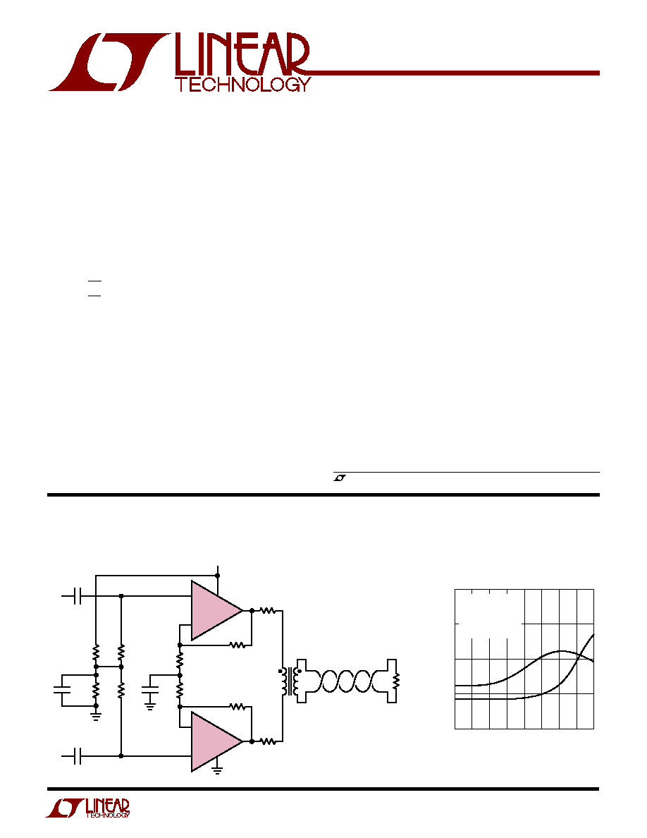
Single 12V Supply ADSL Modem Line Driver
, LTC and LT are registered trademarks of Linear Technology Corporation.
+
1/2 LT1886
12.4
1:2*
12V
909
100
100
20k
10k
IN
IN
+
10k
20k
1
µ
F
1
µ
F
0.1
µ
F
0.1
µ
F
+
1/2 LT1886
12.4
1886 TA01
909
100
*COILCRAFT X8390-A
OR EQUIVALENT
APPLICATIO S
U
FEATURES
TYPICAL APPLICATIO
U
DESCRIPTIO
U
ADSL Modem Line Driver Distortion
LINE VOLTAGE (V
P-P
)
0
HARMONIC DISTORTION (dBc)
60
70
80
90
100
1886 TA01a
2
4
6
8
10
12
14
16
V
S
= 12V
A
V
= 10
f = 200kHz
100
LINE
1:2 TRANSFORMER
HD2
HD3
2
LT1886
W
U
U
PACKAGE/ORDER I FOR ATIO
LT1886CS8
T
JMAX
= 150
°
C,
JA
= 80
°
C/W (Note 4)
ORDER PART
NUMBER
Consult factory for Industrial and Military grade parts.
ELECTRICAL CHARACTERISTICS
The
q
denotes specifications which apply over the full operating temp-
erature range, otherwise specifications are at T
A
= 25
°
C. V
S
=
±
6V, V
CM
= 0V, pulse power tested unless otherwise noted. (Note 9)
SYMBOL
PARAMETER
CONDITIONS
MIN
TYP
MAX
UNITS
V
OS
Input Offset Voltage
(Note 5)
1
4
mV
q
5
mV
Input Offset Voltage Drift
(Note 8)
q
3
17
µ
V/
°
C
I
OS
Input Offset Current
150
400
nA
q
600
nA
I
B
Input Bias Current
1.5
4
µ
A
q
6
µ
A
e
n
Input Noise Voltage
f = 10kHz
6
nV/
Hz
i
n
Input Noise Current
f = 10kHz
2
pA/
Hz
R
IN
Input Resistance
V
CM
=
±
4.5V
5
10
M
Differential
35
k
C
IN
Input Capacitance
2
pF
Input Voltage Range (Positive)
q
4.5
5.9
V
Input Voltage Range (Negative)
q
5.2
4.5
V
CMRR
Common Mode Rejection Ratio
V
CM
=
±
4.5V
q
77
98
dB
Minimum Supply Voltage
Guaranteed by PSRR
q
±
2
V
PSRR
Power Supply Rejection Ratio
V
S
=
±
2V to
±
6.5V
80
86
dB
q
78
dB
A
VOL
Large-Signal Voltage Gain
V
OUT
=
±
4V, R
L
= 100
5.0
12
V/mV
q
4.5
V/mV
V
OUT
=
±
4V, R
L
= 25
4.5
12
V/mV
q
4.0
V/mV
V
OUT
Output Swing
R
L
= 100
, 10mV Overdrive
4.85
5
±
V
q
4.70
±
V
R
L
= 25
, 10mV Overdrive
4.30
4.6
±
V
q
4.10
±
V
I
OUT
= 200mA, 10mV Overdrive
4.30
4.5
±
V
q
4.10
±
V
I
SC
Short-Circuit Current (Sourcing)
(Note 3)
800
mA
Short-Circuit Current (Sinking)
500
mA
S8 PART MARKING
1886
1
2
3
4
8
7
6
5
TOP VIEW
V
+
OUT B
IN B
+IN B
OUT A
IN A
+IN A
V
S8 PACKAGE
8-LEAD PLASTIC SO
B
A
ABSOLUTE
M
AXI
M
U
M
RATINGS
W
W
W
U
(Note 1)
Total Supply Voltage (V
+
to V
) ........................... 13.2V
Input Current (Note 2) .......................................
±
10mA
Input Voltage (Note 2) ............................................
±
V
S
Maximum Continuous Output Current (Note 3)
DC ...............................................................
±
100mA
AC ...............................................................
±
300mA
Operating Temperature Range (Note 10) 40
°
C to 85
°
C
Specified Temperature Range (Note 9) .. 40
°
C to 85
°
C
Maximum Junction Temperature ......................... 150
°
C
Storage Temperature Range ................ 65
°
C to 150
°
C
Lead Temperature (Soldering, 10 sec)................. 300
°
C
3
LT1886
ELECTRICAL CHARACTERISTICS
The
q
denotes specifications which apply over the full operating temp-
erature range, otherwise specifications are at T
A
= 25
°
C. V
S
=
±
6V, V
CM
= 0V, pulse power tested unless otherwise noted. (Note 9)
SYMBOL
PARAMETER
CONDITIONS
MIN
TYP
MAX
UNITS
The
q
denotes specifications which apply over the full operating temperature range, otherwise specifications are at T
A
= 25
°
C.
V
S
=
±
2.5V, V
CM
= 0V, pulse power tested unless otherwise noted. (Note 9)
SYMBOL
PARAMETER
CONDITIONS
MIN
TYP
MAX
UNITS
V
OS
Input Offset Voltage
(Note 5)
1.5
5
mV
q
6
mV
Input Offset Voltage Drift
(Note 8)
q
5
17
µ
V/
°
C
I
OS
Input Offset Current
100
350
nA
q
550
nA
I
B
Input Bias Current
1.2
3.5
µ
A
q
5.5
µ
A
e
n
Input Noise Voltage
f = 10kHz
6
nV/
Hz
i
n
Input Noise Current
f = 10kHz
2
pA/
Hz
R
IN
Input Resistance
V
CM
=
±
1V
10
20
M
Differential
50
k
C
IN
Input Capacitance
2
pF
Input Voltage Range (Positive)
q
1
2.4
V
Input Voltage Range (Negative)
q
1.7
1
V
CMRR
Common Mode Rejection Ratio
V
CM
=
±
1V
q
75
91
dB
A
VOL
Large-Signal Voltage Gain
V
OUT
=
±
1V, R
L
= 100
5.0
10
V/mV
q
4.5
V/mV
V
OUT
=
±
1V, R
L
= 25
4.5
10
V/mV
q
4.0
V/mV
V
OUT
Output Swing
R
L
= 100
, 10mV Overdrive
1.50
1.65
±
V
q
1.40
±
V
R
L
= 25
, 10mV Overdrive
1.35
1.50
±
V
q
1.25
±
V
I
OUT
= 200mA, 10mV Overdrive
0.87
1
±
V
q
0.80
±
V
SR
Slew Rate
A
V
= 10 (Note 6)
133
200
V/
µ
s
q
110
V/
µ
s
Full Power Bandwidth
4V Peak (Note 7)
8
MHz
GBW
Gain Bandwidth
f = 1MHz
700
MHz
t
r
, t
f
Rise Time, Fall Time
A
V
= 10, 10% to 90% of 0.1V, R
L
= 100
4
ns
Overshoot
A
V
= 10, 0.1V, R
L
= 100
1
%
Propagation Delay
A
V
= 10, 50% V
IN
to 50% V
OUT
, 0.1V, R
L
= 100
2.5
ns
t
S
Settling Time
6V Step, 0.1%
50
ns
Harmonic Distortion
HD2, A
V
= 10, 2V
P-P
, f = 1MHz, R
L
= 100
/25
75/ 63
dBc
HD3, A
V
= 10, 2V
P-P
, f = 1MHz, R
L
= 100
/25
85/ 71
dBc
IMD
Intermodulation Distortion
A
V
= 10, f = 0.9MHz, 1MHz, 14dBm, R
L
= 100
/25
81/ 80
dBc
R
OUT
Output Resistance
A
V
= 10, f = 1MHz
0.1
Channel Separation
V
OUT
=
±
4V, R
L
= 25
82
92
dB
q
80
dB
I
S
Supply Current
Per Amplifier
7
8.25
mA
q
8.50
mA
4
LT1886
ELECTRICAL CHARACTERISTICS
The
q
denotes specifications which apply over the full operating temp-
erature range, otherwise specifications are at T
A
= 25
°
C. V
S
=
±
2.5V, V
CM
= 0V, pulse power tested unless otherwise noted. (Note 9)
SYMBOL
PARAMETER
CONDITIONS
MIN
TYP
MAX
UNITS
Note 1: Absolute Maximum Ratings are those values beyond which the life
of a device may be impaired.
Note 2: The inputs are protected by back-to-back diodes. If the differential
input voltage exceeds 0.7V, the input current should be limited to less than
10mA.
Note 3: A heat sink may be required to keep the junction temperature
below absolute maximum.
Note 4: Thermal resistance varies depending upon the amount of PC board
metal attached to the device.
JA
is specified for a 2500mm
2
test board
covered with 2 oz copper on both sides.
Note 5: Input offset voltage is exclusive of warm-up drift.
Note 6: Slew rate is measured between
±
2V on a
±
4V output with
±
6V
supplies, and between
±
1V on a
±
1.5V output with
±
2.5V supplies.
Note 7: Full power bandwidth is calculated from the slew rate:
FPBW = SR/2
V
P
.
Note 8: This parameter is not 100% tested.
Note 9: The LT1886C is guaranteed to meet specified performance from 0
°
C
to 70
°
C. The LT1886C is designed, characterized and expected to meet
specified performance from 40
°
C to 85
°
C but is not tested or QA sampled
at these temperatures. For guaranteed I-grade parts, consult the factory.
Note 10: The LT1886C is guaranteed functional over the operating temperature
range of 40
°
C to 85
°
C.
I
SC
Short-Circuit Current (Sourcing)
(Note 3)
600
mA
Short-Circuit Current (Sinking)
400
mA
SR
Slew Rate
A
V
= 10 (Note 6)
66
100
V/
µ
s
q
60
V/
µ
s
Full Power Bandwidth
1V Peak (Note 7)
16
MHz
GBW
Gain Bandwidth
f = 1MHz
530
MHz
t
r
, t
f
Rise Time, Fall Time
A
V
= 10, 10% to 90% of 0.1V, R
L
= 100
7
ns
Overshoot
A
V
= 10, 0.1V, R
L
= 100
5
%
Propagation Delay
A
V
= 10, 50% V
IN
to 50% V
OUT
, 0.1V, R
L
= 100
5
ns
Harmonic Distortion
HD2, A
V
= 10, 2V
P-P
, f = 1MHz, R
L
= 100
/25
75/ 64
dBc
HD3, A
V
= 10, 2V
P-P
, f = 1MHz, R
L
= 100
/25
80/ 66
dBc
IMD
Intermodulation Distortion
A
V
= 10, f = 0.9MHz, 1MHz, 5dBm, R
L
= 100
/25
77/ 85
dBc
R
OUT
Output Resistance
A
V
= 10, f = 1MHz
0.2
Channel Separation
V
OUT
=
±
1V, R
L
= 25
82
92
dB
q
80
dB
I
S
Supply Current
Per Amplifier
5
5.75
mA
q
6.25
mA
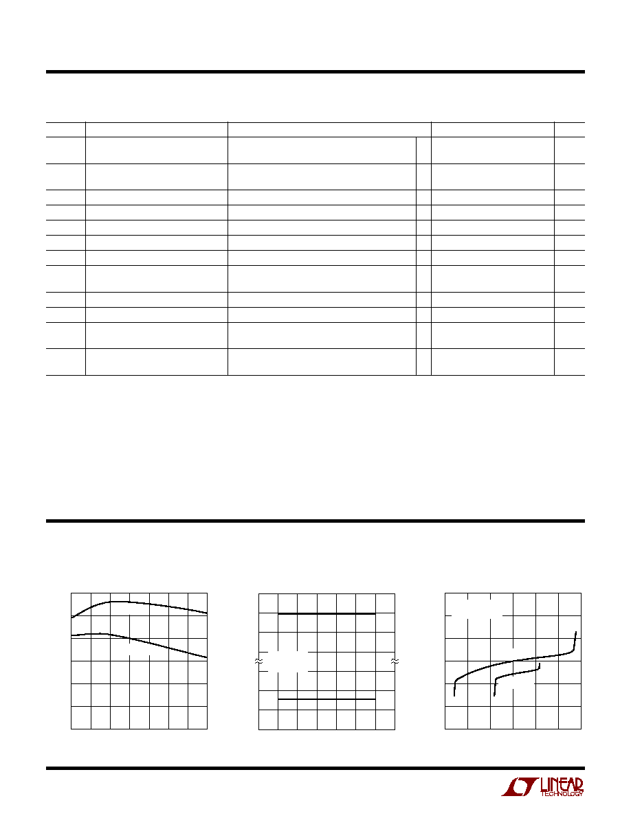
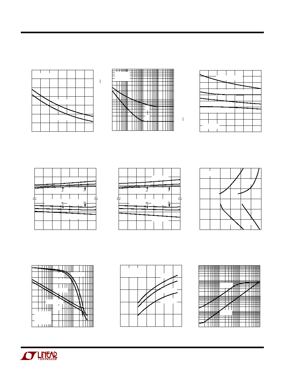
TYPICAL PERFOR A CE CHARACTERISTICS
U
W
Supply Current vs Temperature
Input Common Mode Range vs
Supply Voltage
Input Bias Current vs Input
Common Mode Voltage
TEMPERATURE (
°
C)
50
25
0
25
50
75
100
125
SUPPLY CURRENT (mA)
1886 G01
15
10
5
0
V
S
=
±
6V
V
S
=
±
2.5V
TOTAL SUPPLY VOLTAGE (V)
0
2
4
6
8
10
12
14
COMMON MODE RANGE (V)
1886 G02
V
+
0.1
0.2
0.3
1.5
1.0
0.5
V
T
A
= 25
°
C
V
OS
> 1mV
INPUT COMMON MODE VOLTAGE (V)
6
2
2
4
0
4
6
INPUT BIAS CURRENT (
µ
A)
1886 G03
3.0
2.5
2.0
1.5
1.0
0.5
0
T
A
= 25
°
C
I
B
= (I
B+
+ I
B
)/2
V
S
=
±
6V
V
S
=
±
2.5V
5
LT1886
TYPICAL PERFOR A CE CHARACTERISTICS
U
W
Input Bias Current vs
Temperature
Input Noise Spectral Density
Output Short-Circuit Current vs
Temperature
Output Saturation Voltage vs
Temperature, V
S
=
±
6V
Output Saturation Voltage vs
Temperature, V
S
=
±
2.5V
Settling Time vs Output Step
Gain and Phase vs Frequency
Gain Bandwidth vs Supply
Voltage
Output Impedance vs Frequency
TEMPERATURE (
°
C)
50
25
0
25
50
75
100
125
INPUT BIAS CURRENT (
µ
A)
1886 G04
3.5
3.0
2.5
2.0
1.5
1.0
0.5
0
V
S
=
±
6V
V
S
=
±
2.5V
I
B
= (I
B+
+ I
B
)/2
FREQUENCY (Hz)
10
1
INPUT VOLTAGE NOISE (nV/
Hz)
10
100
INPUT CURRENT NOISE (pA/
Hz)
10
1
100
1k
100k
100
10k
1886 G05
e
n
T
A
= 25
°
C
A
V
= 101
i
n
TEMPERATURE (
°
C)
50
25
0
25
50
75
100
125
OUTPUT SHORT-CIRCUIT CURRENT (mA)
1886 G06
1000
900
800
700
600
500
400
300
200
100
0
SOURCE, V
S
=
±
6V
SOURCE, V
S
=
±
2.5V
SINK, V
S
=
±
6V
SINK, V
S
=
±
2.5V
V
IN
= 0.2V
TEMPERATURE (
°
C)
50
25
0
25
50
75
100
125
OUTPUT SATURATION VOLTAGE (V)
1886 G07
V
+
0.5
1.0
1.5
1.5
1.0
0.5
V
R
L
= 100
R
L
= 100
I
L
= 150mA
I
L
= 200mA
I
L
= 150mA
I
L
= 200mA
TEMPERATURE (
°
C)
50
25
0
25
50
75
100
125
OUTPUT SATURATION VOLTAGE (V)
1886 G08
V
+
0.5
1.0
1.5
1.5
1.0
0.5
V
R
L
= 100
R
L
= 100
I
L
= 150mA
I
L
= 200mA
I
L
= 150mA
I
L
= 200mA
SETTLING TIME (ns)
0
20
40
10
30
50
60
OUTPUT STEP (V)
1886 G09
6
4
2
0
2
4
6
V
S
=
±
6V
10mV
1mV
10mV
1mV
FREQUENCY (Hz)
1M
GAIN (dB)
80
70
60
50
40
30
20
10
0
10
20
PHASE (DEG)
100
80
60
40
20
0
20
40
60
80
100
10M
100M
1G
1886 G10
T
A
= 25
°
C
A
V
= 10
R
L
= 100
V
S
=
±
6V
V
S
=
±
2.5V
V
S
=
±
6V
PHASE
GAIN
V
S
=
±
2.5V
TOTAL SUPPLY VOLTAGE (V)
0
GAIN BANDWIDTH (MHz)
1886 G11
2
4
6
8
10
12
14
800
700
600
500
400
300
T
A
= 25
°
C
A
V
= 10
R
L
= 100
R
L
= 25
R
L
= 1k
FREQUENCY (Hz)
1
0.1
OUTPUT IMPEDANCE (
)
10
100k
10M
100M
1886 G12
0.01
1M
100
A
V
= 100
A
V
= 10