 | ÐлекÑÑоннÑй компоненÑ: LT1920IS8 | СкаÑаÑÑ:  PDF PDF  ZIP ZIP |
Äîêóìåíòàöèÿ è îïèñàíèÿ www.docs.chipfind.ru
1
LT1920
Single Resistor Gain
Programmable, Precision
Instrumentation Amplifier
The LT
®
1920 is a low power, precision instrumentation
amplifier that requires only one external resistor to set gains
of 1 to 10,000. The low voltage noise of 7.5nV/
Hz (at 1kHz)
is not compromised by low power dissipation (0.9mA typical
for
±
2.3V to
±
15V supplies).
The high accuracy of 30ppm maximum nonlinearity and
0.3% max gain error (G = 10) is not degraded even for load
resistors as low as 2k (previous monolithic instrumentation
amps used 10k for their nonlinearity specifications). The
LT1920 is laser trimmed for very low input offset voltage
(125
µ
V max), drift (1
µ
V/
°
C), high CMRR (75dB, G = 1) and
PSRR (80dB, G = 1). Low input bias currents of 2nA max are
achieved with the use of superbeta processing. The output
can handle capacitive loads up to 1000pF in any gain configu-
ration while the inputs are ESD protected up to 13kV (human
body). The LT1920 with two external 5k resistors passes the
IEC 1000-4-2 level 4 specification.
The LT1920, offered in 8-pin PDIP and SO packages, is a pin
for pin and spec for spec improved replacement for the
AD620. The LT1920 is the most cost effective solution for
precision instrumentation amplifier applications. For even
better guaranteed performance, see the LT1167.
s
Single Gain Set Resistor: G = 1 to 10,000
s
Gain Error: G = 10, 0.3% Max
s
Gain Nonlinearity: G = 10, 30ppm Max
s
Input Offset Voltage: G = 10, 225
µ
V Max
s
Input Offset Voltage Drift: 1
µ
V/
°
C Max
s
Input Bias Current: 2nA Max
s
PSRR at G = 1: 80dB Min
s
CMRR at G = 1: 75dB Min
s
Supply Current: 1.3mA Max
s
Wide Supply Range:
±
2.3V to
±
18V
s
1kHz Voltage Noise: 7.5nV/
Hz
s
0.1Hz to 10Hz Noise: 0.28
µ
V
P-P
s
Available in 8-Pin PDIP and SO Packages
s
Meets IEC 1000-4-2 Level 4 ESD Tests with
Two External 5k Resistors
, LTC and LT are registered trademarks of Linear Technology Corporation.
s
Bridge Amplifiers
s
Strain Gauge Amplifiers
s
Thermocouple Amplifiers
s
Differential to Single-Ended Converters
s
Medical Instrumentation
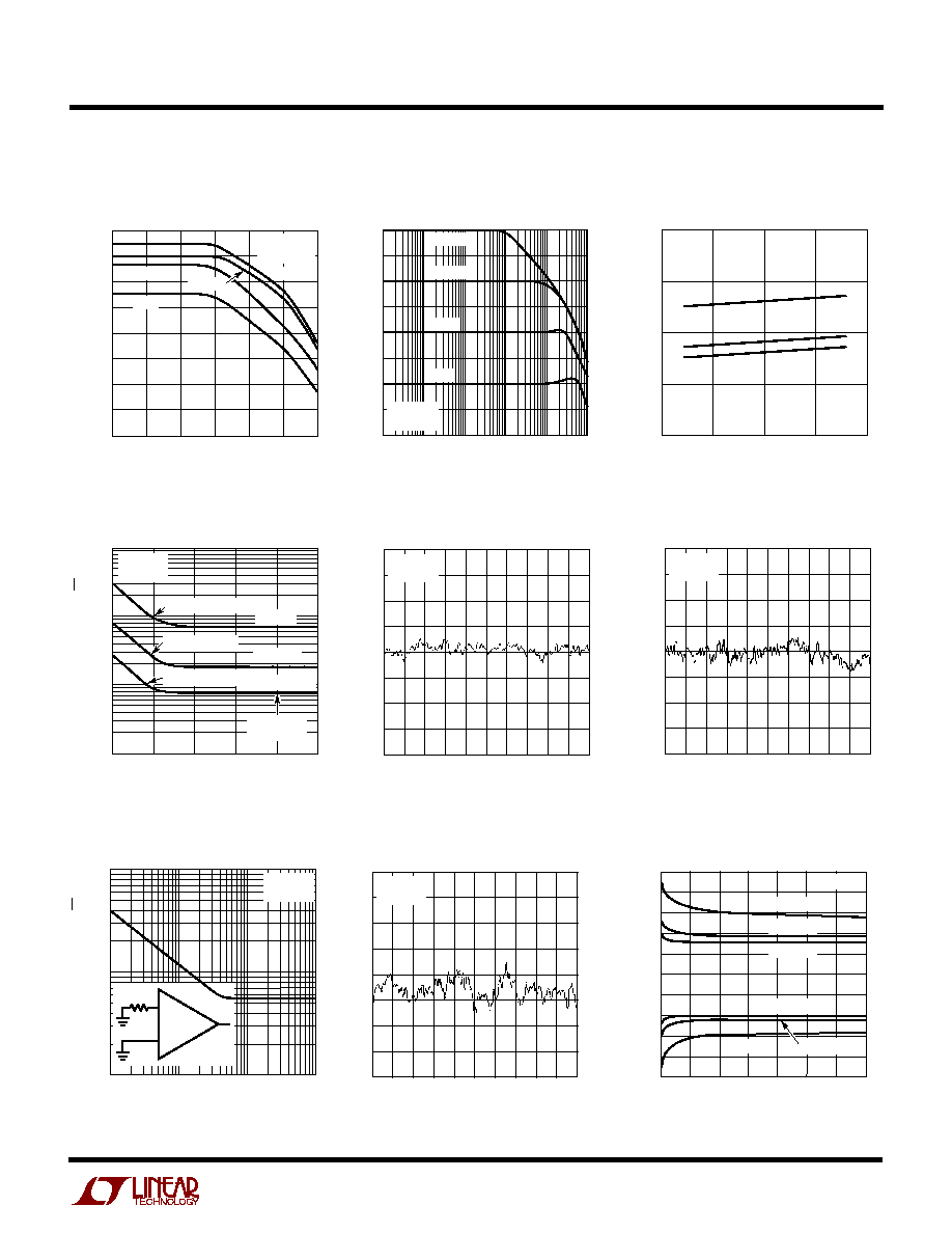
NONLINEARITY (100ppm/DIV)
OUTPUT VOLTAGE (2V/DIV)
G = 1000
R
L
= 1k
V
OUT
=
±
10V
1167 TA02
Gain Nonlinearity
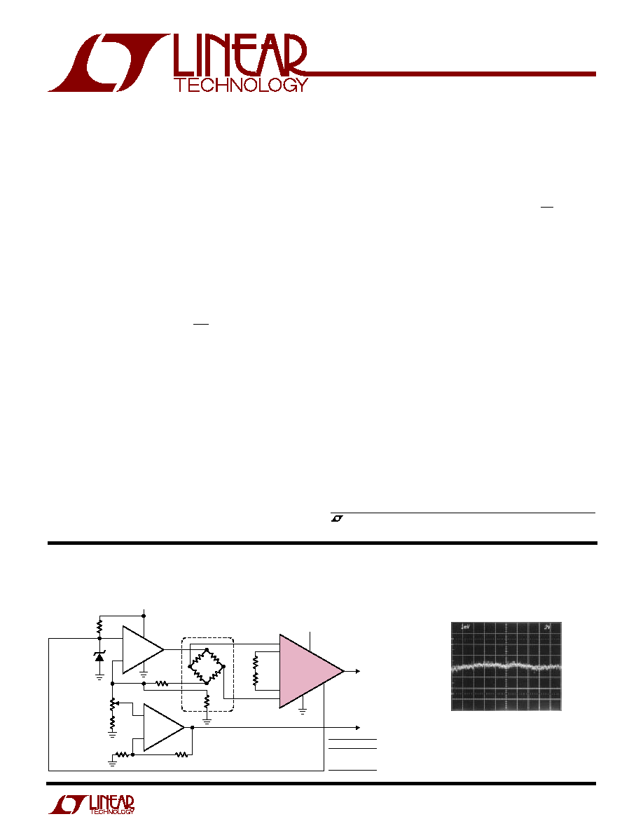
Single Supply Barometer
+
+
+
2
1
1
1
1
2
R5
392k
R4
50k
R3
50k
R8
100k
R6
1k
LT1634CCZ-1.25
8
4
1/2
LT1490
3
R
SET
V
S
= 8V TO 30V
5k
5k
5k
5k
V
S
5
4
3
2
+
7
1/2
LT1490
5
6
2
8
LUCAS NOVA SENOR
NPC-1220-015-A-3L
7
V
S
6
1920 TA01
5
TO
4-DIGIT
DVM
4
R2
12
LT1920
G = 60
R1
825
3
6
R7
50k
VOLTS
2.800
3.000
3.200
INCHES Hg
28.00
30.00
32.00
FEATURES
DESCRIPTIO
U
APPLICATIO S
U
TYPICAL APPLICATIO
U
2
LT1920
ABSOLUTE
M
AXI
M
U
M
RATINGS
W
W
W
U
ORDER PART
NUMBER
PACKAGE/ORDER I
N
FOR
M
ATIO
N
W
U
U
LT1920CN8
LT1920CS8
LT1920IN8
LT1920IS8
S8 PART MARKING
1920
1920I
1
2
3
4
8
7
6
5
TOP VIEW
R
G
IN
+IN
V
S
R
G
+V
S
OUTPUT
REF
N8 PACKAGE
8-LEAD PDIP
S8 PACKAGE
8-LEAD PLASTIC SO
+
T
JMAX
= 150
°
C,
JA
= 130
°
C/ W (N8)
T
JMAX
= 150
°
C,
JA
= 190
°
C/ W (S8)
(Note 1)
Supply Voltage ......................................................
±
20V
Differential Input Voltage (Within the
Supply Voltage) .....................................................
±
40V
Input Voltage (Equal to Supply Voltage) ................
±
20V
Input Current (Note 3) ........................................
±
20mA
Output Short-Circuit Duration .......................... Indefinite
Operating Temperature Range ................ 40
°
C to 85
°
C
Specified Temperature Range
LT1920C (Note 4) .................................... 0
°
C to 70
°
C
LT1920I .............................................. 40
°
C to 85
°
C
Storage Temperature Range ................. 65
°
C to 150
°
C
Lead Temperature (Soldering, 10 sec).................. 300
°
C
Consult factory for Military grade parts.
ELECTRICAL CHARACTERISTICS
V
S
=
±
15V, V
CM
= 0V, T
A
= 25
°
C, R
L
= 2k, unless otherwise noted.
SYMBOL
PARAMETER
CONDITIONS (Note 6)
MIN
TYP
MAX
UNITS
G
Gain Range
G = 1 + (49.4k/R
G
)
1
10k
Gain Error
G = 1
0.008
0.1
%
G = 10 (Note 2)
0.010
0.3
%
G = 100 (Note 2)
0.025
0.3
%
G = 1000 (Note 2)
0.040
0.35
%
G/T
Gain vs Temperature
G < 1000 (Note 2)
q
20
50
ppm/
°
C
Gain Nonlinearity (Note 5)
V
O
=
±
10V, G = 1
10
ppm
V
O
=
±
10V, G = 10 and 100
10
30
ppm
V
O
=
±
10V, G = 100 and 1000
20
ppm
V
OST
Total Input Referred Offset Voltage
V
OST
= V
OSI
+ V
OSO
/G
V
OSI
Input Offset Voltage
G = 1000, V
S
=
±
5V to
±
15V
30
125
µ
V
G = 1000, V
S
=
±
5V to
±
15V
q
185
µ
V
V
OSI
/T
Input Offset Drift (RTI)
(Note 3)
q
1
µ
V/
°
C
V
OSO
Output Offset Voltage
G = 1, V
S
=
±
5V to
±
15V
400
1000
µ
V
G = 1, V
S
=
±
5V to
±
15V
q
1500
µ
V
V
OSO
/T
Output Offset Drift
(Note 3)
q
5
15
µ
V/
°
C
I
OS
Input Offset Current
0.3
1
nA
I
B
Input Bias Current
0.5
2
nA
e
n
Input Noise Voltage, RTI
0.1Hz to 10Hz, G = 1
2.00
µ
V
P-P
0.1Hz to 10Hz, G = 10
0.50
µ
V
P-P
0.1Hz to 10Hz, G = 100 and 1000
0.28
µ
V
P-P
Total RTI Noise =
e
ni
2
+ (e
no
/G)
2
e
ni
Input Noise Voltage Density, RTI
f
O
= 1kHz
7.5
nV/
Hz
e
no
Output Noise Voltage Density, RTI
f
O
= 1kHz
67
nV/
Hz
i
n
Input Noise Current
f
O
= 0.1Hz to 10Hz
10
pA
P-P
Input Noise Current Density
f
O
= 10Hz
124
fA/
Hz
R
IN
Input Resistance
V
IN
=
±
10V
200
G
C
IN(DIFF)
Differential Input Capacitance
f
O
= 100kHz
1.6
pF
3
LT1920
ELECTRICAL CHARACTERISTICS
V
S
=
±
15V, V
CM
= 0V, T
A
= 25
°
C, R
L
= 2k, unless otherwise noted.
SYMBOL
PARAMETER
CONDITIONS (Note 6)
MIN
TYP
MAX
UNITS
C
IN(CM)
Common Mode Input Capacitance
f
O
= 100kHz
1.6
pF
V
CM
Input Voltage Range
G = 1, Other Input Grounded
V
S
=
±
2.3V to
±
5V
V
S
+ 1.9
+V
S
1.2
V
V
S
=
±
5V to
±
18V
V
S
+ 1.9
+V
S
1.4
V
V
S
=
±
2.3V to
±
5V
q
V
S
+ 2.1
+V
S
1.3
V
V
S
=
±
5V to
±
18V
q
V
S
+ 2.1
+V
S
1.4
V
CMRR
Common Mode Rejection Ratio
1k Source Imbalance,
V
CM
= 0V to
±
10V
G = 1
75
95
dB
G = 10
95
115
dB
G = 100
110
125
dB
G = 1000
110
140
dB
PSRR
Power Supply Rejection Ratio
V
S
=
±
2.3 to
±
18V
G = 1
80
120
dB
G = 10
100
135
dB
G = 100
120
140
dB
G = 1000
120
150
dB
I
S
Supply Current
V
S
=
±
2.3V to
±
18V
0.9
1.3
mA
V
OUT
Output Voltage Swing
R
L
= 10k
V
S
=
±
2.3V to
±
5V
V
S
+ 1.1
+V
S
1.2
V
V
S
=
±
5V to
±
18V
V
S
+ 1.2
+V
S
1.3
V
V
S
=
±
2.3V to
±
5V
q
V
S
+ 1.4
+V
S
1.3
V
V
S
=
±
5V to
±
18V
q
V
S
+ 1.6
+V
S
1.5
V
I
OUT
Output Current
20
27
mA
BW
Bandwidth
G = 1
1000
kHz
G = 10
800
kHz
G = 100
120
kHz
G = 1000
12
kHz
SR
Slew Rate
G = 1, V
OUT
=
±
10V
1.2
V/
µ
s
Settling Time to 0.01%
10V Step
G = 1 to 100
14
µ
s
G = 1000
130
µ
s
R
REFIN
Reference Input Resistance
20
k
I
REFIN
Reference Input Current
V
REF
= 0V
50
µ
A
V
REF
Reference Voltage Range
V
S
+ 1.6
+V
S
1.6
V
A
VREF
Reference Gain to Output
1
±
0.0001
The
q
denotes specifications that apply over the full specified
temperature range.
Note 1: Absolute Maximum Ratings are those values beyond which the life
of a device may be impaired.
Note 2: Does not include the effect of the external gain resistor R
G
.
Note 3: This parameter is not 100% tested.
Note 4: The LT1920C is designed, characterized and expected to meet the
industrial temperature limits, but is not tested at 40
°
C and 85
°
C. I-grade
parts are guaranteed.
Note 5: This parameter is measured in a high speed automatic tester that
does not measure the thermal effects with longer time constants. The
magnitude of these thermal effects are dependent on the package used,
heat sinking and air flow conditions.
Note 6: Typical parameters are defined as the 60% of the yield parameter
distribution.
4
LT1920
TYPICAL PERFOR A CE CHARACTERISTICS
U
W
Gain Nonlinearity, G = 1
NONLINEARITY (1ppm/DIV)
OUTPUT VOLTAGE (2V/DIV)
G = 1
R
L
= 2k
V
OUT
=
±
10V
1167 G01
Gain Nonlinearity, G = 10
NONLINEARITY (10ppm/DIV)
OUTPUT VOLTAGE (2V/DIV)
1167 G02
G = 10
R
L
= 2k
V
OUT
=
±
10V
Gain Nonlinearity, G = 100
NONLINEARITY (10ppm/DIV)
OUTPUT VOLTAGE (2V/DIV)
G = 100
R
L
= 2k
V
OUT
=
±
10V
1167 G03
Gain Nonlinearity, G = 1000
NONLINEARITY (100ppm/DIV)
OUTPUT VOLTAGE (2V/DIV)
G = 1000
R
L
= 2k
V
OUT
=
±
10V
1167 G04
Warm-Up Drift
TIME AFTER POWER ON (MINUTES)
0
10
12
S8
N8
14
3
4
1920
G09
8
6
1
2
5
4
2
0
CHANGE IN OFFSET VOLTAGE (
µ
V)
V
S
=
±
15V
T
A
= 25
°
C
G = 1
Gain Error vs Temperature
TEMPERATURE (
°
C)
50
GAIN ERROR (%)
0.20
0.10
0.05
0
50
0.20
1920
G06
0.15
0
25
75
G = 1
25
100
0.05
0.10
0.15
V
S
=
±
15V
V
OUT
=
±
10V
R
L
= 2k
*DOES NOT INCLUDE
TEMPERATURE EFFECTS
OF R
G
G = 10*
G = 1000*
G = 100*
FREQUENCY (Hz)
0.1
COMMON MODE REJECTION RATIO (dB)
60
80
100
100
10k
1920 G14
40
20
0
1
10
1k
120
140
160
100k
G = 1000
G = 100
G = 10
G = 1
V
S
=
±
15V
T
A
= 25
°
C
1k SOURCE
IMBALANCE
Common Mode Rejection Ratio
vs Frequency
FREQUENCY (Hz)
0.1
NEGATIVE POWER SUPPLY REJECTION RATIO (dB)
60
80
100
100
10k
1920 G15
40
20
0
1
10
1k
120
140
160
100k
G = 1000
G = 100
G = 10
G = 1
V
+
= 15V
T
A
= 25
°
C
Negative Power Supply Rejection
Ratio vs Frequency
COMMON MODE INPUT VOLTAGE (V)
15
INPUT BIAS CURRENT (pA)
100
300
500
9
1920 G13
100
300
0
200
400
200
400
500
9
3
3
12
12
6
0
6
15
40
°
C
85
°
C
0
°
C
70
°
C
25
°
C
Input Bias Current
vs Common Mode Input Voltage
5
LT1920
TYPICAL PERFOR A CE CHARACTERISTICS
U
W
FREQUENCY (Hz)
0.1
POSITIVE POWER SUPPLY REJECTION RATIO (dB)
60
80
100
100
10k
1920 G16
40
20
0
1
10
1k
120
140
160
100k
G = 1000
G = 10
G = 1
V
= 15V
T
A
= 25
°
C
G = 100
Positive Power Supply Rejection
Ratio vs Frequency
Gain vs Frequency
FREQUENCY (kHz)
0
GAIN (dB)
10
30
50
60
0.01
1
10
1000
1920 G17
10
0.1
100
40
20
20
G = 1000
G = 100
G = 10
G = 1
V
S
=
±
15V
T
A
= 25
°
C
Supply Current vs Supply Voltage
SUPPLY VOLTAGE (
±
V)
0
SUPPLY CURRENT (mA)
1.00
1.25
85
°
C
25
°
C
40
°
C
20
1920 G18
0.75
0.50
5
10
15
1.50
0.1Hz to 10Hz Noise Voltage, RTI
G = 1000
TIME (SEC)
0
NOISE VOLTAGE (0.2
µ
V/DIV)
8
1920 G21
2
4
5
10
6
1
3
9
7
V
S
=
±
15V
T
A
= 25
°
C
FREQUENCY (Hz)
1
0
100
1000
10
100
1k
100k
10k
1920
G19
10
VOLTAGE NOISE DENSITY (nV
Hz)
V
S
=
±
15V
T
A
= 25
°
C
1/f
CORNER
= 10Hz
1/f
CORNER
= 9Hz
1/f
CORNER
= 7Hz
GAIN = 1
GAIN = 10
GAIN = 100, 1000
BW LIMIT
GAIN = 1000
Voltage Noise Density
vs Frequency
TIME (SEC)
0
NOISE VOLTAGE (2
µ
V/DIV)
8
1920 G20
2
4
5
10
6
1
3
9
7
V
S
=
±
15V
T
A
= 25
°
C
0.1Hz to 10Hz Noise Voltage,
G = 1
Current Noise Density
vs Frequency
FREQUENCY (Hz)
1
10
CURRENT NOISE DENSITY (fA/
Hz)
100
1000
10
100
1000
1920
G22
V
S
=
±
15V
T
A
= 25
°
C
R
S
TIME FROM OUTPUT SHORT TO GROUND (MINUTES)
0
50
(SINK)
(SOURCE)
OUTPUT CURRENT (mA)
40
20
10
0
50
20
1
2
1920 G24
30
30
40
10
3
T
A
= 40
°
C
V
S
=
±
15V
T
A
= 40
°
C
T
A
= 25
°
C
T
A
= 85
°
C
T
A
= 85
°
C
T
A
= 25
°
C
Short-Circuit Current vs Time
TIME (SEC)
0
CURRENT NOISE (5pA/DIV)
8
1920 G23
2
4
5
10
6
1
3
9
7
V
S
=
±
15V
T
A
= 25
°
C
0.1Hz to 10Hz Current Noise