1956f.pm6
1
LT1956/LT1956-5
1956f
High Voltage, 1.5A,
500kHz Step-Down
Switching Regulators
s
Wide Input Range: 5.5V to 60V
s
1.5A Peak Switch Current
s
Small 16-Pin SSOP or Thermally Enhanced
TSSOP Package
s
Saturating Switch Design: 0.2
s
Peak Switch Current Maintained Over
Full Duty Cycle Range
s
Constant 500kHz Switching Frequency
s
Effective Supply Current: 2.5mA
s
Shutdown Current: 25
µ
A
s
1.2V Feedback Reference (LT1956)
s
5V Fixed Output (LT1956-5)
s
Easily Synchronizable
s
Cycle-by-Cycle Current Limiting
The LT
®
1956/LT1956-5 are 500kHz monolithic buck
switching regulators with an input voltage capability up to
60V. A high efficiency 1.5A, 0.2
switch is included on the
die along with all the necessary oscillator, control and logic
circuitry. A current mode architecture provides fast tran-
sient response and good loop stability.
Special design techniques and a new high voltage process
achieve high efficiency over a wide input range. Efficiency
is maintained over a wide output current range by using the
output to bias the circuitry and by utilizing a supply boost
capacitor to saturate the power switch. Patented circuitry
maintains peak switch current over the full duty cycle
range*. A shutdown pin reduces supply current to 25
µ
A and
the device can be externally synchronized from 580kHz to
700kHz with a logic level input.
The LT1956/LT1956-5 are available in fused-lead 16-pin
SSOP and thermally enhanced TSSOP packages.
s
High Voltage, Industrial and Automotive
s
Portable Computers
s
Battery-Powered Systems
s
Battery Chargers
s
Distributed Power Systems
, LTC and LT are registered trademarks of Linear Technology Corporation.
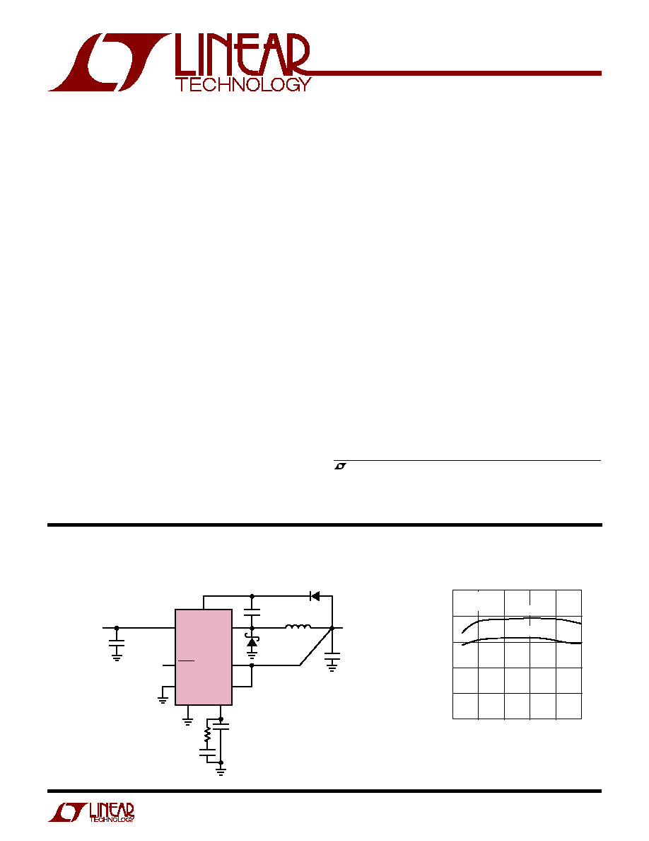
5V Buck Converter
Efficiency vs Load Current
BOOST
V
IN
6
2
10
12
10MQ060N
V
OUT
5V
1A
4
15
14
11
220pF
4700pF
UNITED CHEMI-CON THCS50EZA225ZT
1, 8, 9, 16
LT1956-5
SHDN
SYNC
SW
BIAS
FB
V
C
GND
0.1
µ
F
22
µ
F
6.3V
CERAMIC
10
µ
H
MMSD914TI
1956 TA01
2.2
µ
F
100V
CERAMIC
V
IN
12V
(TRANSIENTS
TO 60V)
4.7k
LOAD CURRENT (A)
0
EFFICIENCY (%)
80
90
100
1.00
1956 TA02
70
60
50
0.25
0.50
0.75
1.25
V
OUT
= 5V
V
OUT
= 3.3V
V
IN
= 12V
L = 18
µ
H
DESCRIPTIO
U
FEATURES
APPLICATIO S
U
TYPICAL APPLICATIO
U
*U.S. PATENT NO. 6,498,466
2
LT1956/LT1956-5
1956f
Input Voltage (V
IN
) ................................................. 60V
BOOST Pin Above SW ............................................ 35V
BOOST Pin Voltage ................................................. 68V
SYNC, SENSE Voltage (LT1956-5) ........................... 7V
SHDN Voltage ........................................................... 6V
BIAS Pin Voltage .................................................... 30V
FB Pin Voltage/Current (LT1956) ................... 3.5V/2mA
ORDER PART
NUMBER
LT1956EGN
LT1956IGN
LT1956EGN-5
LT1956IGN-5
GN PART MARKING
1956
1956I
19565
1956I5
T
JMAX
= 125
°
C,
JA
= 85
°
C/ W,
JC
(PIN 8) = 25
°
C/ W
FOUR CORNER PINS SOLDERED
TO GROUND PLANE
ABSOLUTE AXI U RATI GS
W
W
W
U
PACKAGE/ORDER I FOR ATIO
U
U
W
GN PACKAGE
16-LEAD PLASTIC SSOP
1
2
3
4
5
6
7
8
TOP VIEW
16
15
14
13
12
11
10
9
GND
SW
NC
V
IN
NC
BOOST
NC
GND
GND
SHDN
SYNC
NC
FB/SENSE
V
C
BIAS
GND
Operating Junction Temperature Range
LT1956EFE/LT1956EFE-5/LT1956EGN/LT1956EGN-5
(Notes 8, 10) ..................................... 40
°
C to 125
°
C
LT1956IFE/LT1956IFE-5/LT1956IGN/LT1956IGN-5
(Notes 8, 10) ..................................... 40
°
C to 125
°
C
Storage Temperature Range ................ 65
°
C to 150
°
C
Lead Temperature (Soldering, 10 sec)................. 300
°
C
(Note 1)
ORDER PART
NUMBER
LT1956EFE
LT1956IFE
LT1956EFE-5
LT1956IFE-5
FE PART MARKING
T
JMAX
= 125
°
C,
JA
= 45
°
C/ W,
JC
(PAD) = 10
°
C/ W
EXPOSED BACKSIDE MUST BE SOLDERED
TO GROUND PLANE
FE PACKAGE
16-LEAD PLASTIC TSSOP
1
2
3
4
5
6
7
8
TOP VIEW
16
15
14
13
12
11
10
9
GND
SW
NC
V
IN
NC
BOOST
NC
GND
GND
SHDN
SYNC
NC
FB/SENSE
V
C
BIAS
GND
Consult LTC Marketing for parts specified with wider operating temperature ranges.
PARAMETER
CONDITIONS
MIN
TYP
MAX
UNITS
Reference Voltage (LT1956)
5.5V
V
IN
60V
1.204
1.219
1.234
V
V
OL
+ 0.2
V
C
V
OH
0.2
q
1.195
1.243
V
SENSE Voltage (LT1956-5)
5.5V
V
IN
60V
4.94
5
5.06
V
V
OL
+ 0.2
V
C
V
OH
0.2
q
4.90
5.10
V
SENSE Pin Resistance (LT1956-5)
9.5
13.8
19
k
FB Input Bias Current (LT1956)
q
0.5
1.5
µ
A
Error Amp Voltage Gain
(Notes 2, 9)
200
400
V/V
Error Amp g
m
dl (V
C
) =
±
10
µ
A (Note 9)
1500
2000
3000
µ
Mho
q
1000
3200
µ
Mho
V
C
to Switch g
m
1.7
A/V
EA Source Current
FB = 1V or V
SENSE
= 4.1V
q
125
225
400
µ
A
EA Sink Current
FB = 1.4V or V
SENSE
= 5.7V
q
100
225
450
µ
A
V
C
Switching Threshold
Duty Cycle = 0
0.9
V
V
C
High Clamp
SHDN = 1V
2.1
V
The
q
denotes specifications which apply over the full operating temperature range, otherwise specifications are at T
J
= 25
°
C.
V
IN
= 15V, V
C
= 1.5V, SHDN = 1V, Boost o/c, SW o/c, unless otherwise noted.
ELECTRICAL CHARACTERISTICS
1956EFE
1956IFE
1956EFE-5
1956IFE-5
3
LT1956/LT1956-5
1956f
PARAMETER
CONDITIONS
MIN
TYP
MAX
UNITS
Switch Current Limit
V
C
Open, Boost = V
IN
+ 5V, FB = 1V or V
SENSE
= 4.1V
q
1.5
2
3
A
Switch On Resistance
I
SW
= 1.5A, Boost = V
IN
+ 5V (Note 7)
0.2
0.3
q
0.4
Maximum Switch Duty Cycle
FB = 1V or V
SENSE
= 4.1V
82
90
%
q
75
90
%
Switch Frequency
V
C
Set to Give DC = 50%
460
500
540
kHz
q
430
570
kHz
f
SW
Line Regulation
5.5V
V
IN
60V
q
0.05
0.15
%/V
f
SW
Shifting Threshold
Df = 10kHz
0.8
V
Minimum Input Voltage
(Note 3)
q
4.6
5.5
V
Minimum Boost Voltage
(Note 4) I
SW
1.5A
q
2
3
V
Boost Current (Note 5)
Boost = V
IN
+ 5V, I
SW
= 0.5A
q
12
25
mA
Boost = V
IN
+ 5V, I
SW
= 1.5A
q
42
70
mA
Input Supply Current (I
VIN
)
(Note 6) V
BIAS
= 5V
1.4
2.2
mA
Output Supply Current (I
BIAS
)
(Note 6) V
BIAS
= 5V
2.9
4.2
mA
Shutdown Supply Current
SHDN = 0V, V
IN
60V, SW = 0V, V
C
Open
25
75
µ
A
q
200
µ
A
Lockout Threshold
V
C
Open
q
2.30
2.42
2.53
V
Shutdown Thresholds
V
C
Open, Shutting Down
q
0.15
0.37
0.6
V
V
C
Open, Starting Up
q
0.25
0.45
0.6
V
Minimum SYNC Amplitude
q
1.5
2.2
V
SYNC Frequency Range
580
700
kHz
SYNC Input Resistance
20
k
The
q
denotes specifications which apply over the full operating temperature range, otherwise specifications are at T
J
= 25
°
C.
V
IN
= 15V, V
C
= 1.5V, SHDN = 1V, Boost o/c, SW o/c, unless otherwise noted.
ELECTRICAL CHARACTERISTICS
Note 1: Absolute Maximum Ratings are those values beyond which the life
of a device may be impaired.
Note 2: Gain is measured with a V
C
swing equal to 200mV above the low
clamp level to 200mV below the upper clamp level.
Note 3: Minimum input voltage is not measured directly, but is guaranteed
by other tests. It is defined as the voltage where internal bias lines are still
regulated so that the reference voltage and oscillator remain constant.
Actual minimum input voltage to maintain a regulated output will depend
upon output voltage and load current. See Applications Information.
Note 4: This is the minimum voltage across the boost capacitor needed to
guarantee full saturation of the internal power switch.
Note 5: Boost current is the current flowing into the BOOST pin with the
pin held 5V above input voltage. It flows only during switch on time.
Note 6: Input supply current is the quiescent current drawn by the input
pin when the BIAS pin is held at 5V with switching disabled. Bias supply
current is the current drawn by the BIAS pin when the BIAS pin is held at
5V. Total input referred supply current is calculated by summing input
supply current (I
VIN
) with a fraction of supply current (I
BIAS
):
I
TOTAL
= I
VIN
+ (I
BIAS
)(V
OUT
/V
IN
)
with V
IN
= 15V, V
OUT
= 5V, I
VIN
= 1.4mA, I
BIAS
= 2.9mA, I
TOTAL
= 2.4mA.
Note 7: Switch on resistance is calculated by dividing V
IN
to SW voltage by
the forced current (1.5A). See Typical Performance Characteristics for the
graph of switch voltage at other currents.
Note 8: The LT1956EFE/LT1956EFE-5/LT1956EGN/LT1956EGN-5 are
guaranteed to meet performance specifications from 0
°
C to 125
°
C
junction temperature. Specifications over the 40
°
C to 125
°
C operating
junction temperature range are assured by design, characterization and
correlation with statistical process controls. The LT1956IFE/LT1956IFE-5/
LT1956IGN/LT1956IGN-5 are guaranteed over the full 40
°
C to 125
°
C
operating junction temperature range.
Note 9: Transconductance and voltage gain refer to the internal amplifier
exclusive of the voltage divider. To calculate gain and transconductance,
refer to the SENSE pin on fixed voltage parts. Divide values shown by the
ratio V
OUT
/1.219.
Note 10: This IC includes overtemperature protection that is intended to
protect the device during momentary overload conditions. Junction
temperature will exceed 125
°
C when overtemperature protection is active.
Continuous operation above the specified maximum operating junction
temperature may impair device reliability.
4
LT1956/LT1956-5
1956f
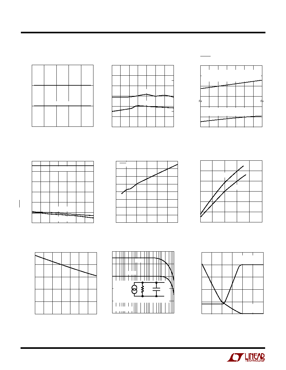
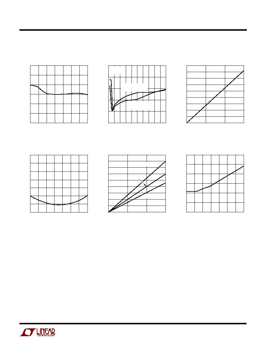
Switch Peak Current Limit
SHDN Pin Bias Current
Shutdown Supply Current
Lockout and Shutdown
Thresholds
Shutdown Supply Current
Error Amplifier Transconductance
FB Pin Voltage and Current
Error Amplifier Transconductance
Frequency Foldback
TYPICAL PERFOR A CE CHARACTERISTICS
U
W
DUTY CYCLE (%)
1.0
SWITCH PEAK CURRENT (A)
1.5
2.0
2.5
20
40
TYPICAL
60
80
1956 G01
100
0
GUARANTEED MINIMUM
JUNCTION TEMPERATURE (
°
C)
50
FEEDBACK VOLTAGE (V)
CURRENT (
µ
A)
1.224
1.229
1.234
25
75
1956 G02
1.219
1.214
25
0
50
100
125
1.209
1.204
1.5
2.0
1.0
0.5
0
VOLTAGE
CURRENT
JUNCTION TEMPERATURE (
°
C)
50
250
200
150
100
12
6
0
25
75
1956 G03
25
0
50
100
125
CURRENT (
µ
A)
CURRENT REQUIRED TO FORCE SHUTDOWN
(FLOWS OUT OF PIN). AFTER SHUTDOWN,
CURRENT DROPS TO A FEW
µ
A
AT 2.38V STANDBY THRESHOLD
(CURRENT FLOWS OUT OF PIN)
JUNCTION TEMPERATURE (
°
C)
50
SHDN PIN VOLTAGE (V)
50
100
1956
G04
0
25
75
2.4
2.0
1.6
1.2
0.8
0.4
0
25
125
LOCKOUT
START-UP
SHUTDOWN
INPUT VOLTAGE (V)
0
INPUT SUPPLY CURRENT (
µ
A)
1956
G05
10
20
30
40
50
60
40
35
30
25
20
15
10
5
0
V
SHDN
= 0V
SHUTDOWN VOLTAGE (V)
0
0
INPUT SUPPLY CURRENT (
µ
A)
50
100
150
200
250
300
0.1
0.2
0.3
0.4
1956
G06
0.5
V
IN
= 60V
V
IN
= 15V
JUNCTION TEMPERATURE
TRANSCONDUCTANCE (
µ
mho)
1956
G07
2500
2000
1500
1000
500
0
50
50
100
0
25
75
25
125
FREQUENCY (Hz)
GAIN (
µ
Mho)
PHASE (DEG)
3000
2500
2000
1500
1000
500
200
150
100
50
0
50
100
10k
100k
10M
1956
G08
1k
1M
GAIN
PHASE
ERROR AMPLIFIER EQUIVALENT CIRCUIT
R
OUT
200k
C
OUT
12pF
V
C
R
LOAD
= 50
V
FB
2 ·
10
3
)
(
V
FB
(V)
0
0.2
SWITICHING FREQUENCY (kHz)
OR FB CURRENT (
µ
A)
375
500
625
1.0
1956
G09
250
125
0
0.4
0.6
0.8
1.2
SWITCHING
FREQUENCY
FB PIN
CURRENT
5
LT1956/LT1956-5
1956f
Switching Frequency
BOOST Pin Current
V
C
Pin Shutdown Threshold
Minimum Input Voltage with 5V
Output
Switch Voltage Drop
TYPICAL PERFOR A CE CHARACTERISTICS
U
W
JUNCTION TEMPERATURE (
°
C)
50
FREQUENCY (kHz)
50
100
1956
G10
0
25
75
575
550
525
500
475
450
425
25
125
LOAD CURRENT (A)
0
INPUT VOLTAGE (V)
1956
G11
0.1 0.2 0.3 0.4 0.5 0.6 0.7 0.8 0.9
1
7.5
7.0
6.5
6.0
5.5
5.0
MINIMUM INPUT
VOLTAGE TO START
MINIMUM INPUT
VOLTAGE TO RUN
V
OUT
= 5V
L = 18
µ
H
SWITCH CURRENT (A)
0
0.5
1
1.5
BOOST PIN CURRENT (mA)
1956 G12
45
40
35
30
25
20
15
10
5
0
JUNCTION TEMPERATURE (
°
C)
50
1.5
1.7
2.1
25
75
1956
G13
1.3
1.1
25
0
50
100
125
0.9
0.7
1.9
THRESHOLD VOLTAGE (V)
SWITCH CURRENT (A)
0
0.5
1
1.5
SWITCH VOLTAGE (mV)
1766 G14
450
400
350
300
250
200
150
100
50
0
T
J
= 125
°
C
T
J
= 25
°
C
T
J
= 40
°
C
JUNCTION TEMPERATURE (
°
C)
50
SWITCH MINIMUM ON TIME (ns)
50
100
1956
G15
0
25
75
600
500
400
300
200
100
0
25
125
Switch Minimum ON Time
vs Temperature