Äîêóìåíòàöèÿ è îïèñàíèÿ www.docs.chipfind.ru
LT1964
1
1964f
s
Battery-Powered Instruments
s
Low Noise Regulator for Noise-Sensitive
Instrumentation
s
Negative Complement to LT1761 Family of
Positive LDOs
s
Low Profile (1mm) ThinSOT
TM
Package
s
Low Noise: 30
µ
V
RMS
(10Hz to 100kHz)
s
Low Quiescent Current: 30
µ
A
s
Low Dropout Voltage: 340mV
s
Output Current: 200mA
s
Fixed Output Voltage: 5V
s
Adjustable Output from 1.22V to 20V
s
Positive or Negative Shutdown Logic
s
3
µ
A Quiescent Current in Shutdown
s
Stable with 1
µ
F Output Capacitor
s
Stable with Aluminum, Tantalum, or Ceramic
Capacitors
s
Thermal Limiting
200mA, Low Noise,
Low Dropout Negative
Micropower Regulator in ThinSOT
The LT
®
1964 is a micropower low noise, low dropout
negative regulator. The device is capable of supplying
200mA of output current with a dropout voltage of 340mV.
Low quiescent current (30
µ
A operating and 3
µ
A shut-
down) makes the LT1964 an excellent choice for battery-
powered applications. Quiescent current is well controlled
in dropout.
Other features of the LT1964 include low output noise.
With the addition of an external 0.01
µ
F bypass capacitor,
output noise is reduced to 30
µ
V
RMS
over a 10Hz to 100kHz
bandwidth. The LT1964 is capable of operating with small
capacitors and is stable with output capacitors as low as
1
µ
F. Small ceramic capacitors can be used without the
necessary addition of ESR as is common with other
regulators. Internal protection circuitry includes reverse
output protection, current limiting, and thermal limiting.
The device is available with a fixed output voltage of 5V
and as an adjustable device with a 1.22V reference
voltage. The LT1964 regulators are available in a low
profile (1mm) ThinSOT package.
, LTC and LT are registered trademarks of Linear Technology Corporation.
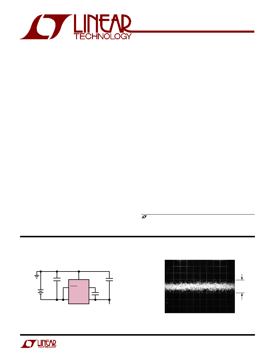
1964 TA01a
GND
SHDN
BYP
IN
OUT
LT1964-5
1
µ
F
10
µ
F
0.01
µ
F
V
IN
5.4V
TO 20V
5V AT 200mA
30
µ
V
RMS
NOISE
5V Low Noise Regulator
10Hz to 100kHz Output Noise
V
OUT
100
µ
V/DIV
1ms/DIV
1964 TA01b
30
µ
V
RMS
ThinSOT is a trademark of Linear Technology Corporation.
APPLICATIO S
U
FEATURES
TYPICAL APPLICATIO
U
DESCRIPTIO
U
LT1964
2
1964f
SHDN Pin Voltage
(with Respect to GND Pin) ........................ 20V, 15V
Output Short-Circuit Duration .......................... Indefinite
Operating Junction Temperature
Range (Note 10) ............................... 40
°
C to 125
°
C
Storage Temperature Range ................. 65
°
C to 150
°
C
Lead Temperature (Soldering, 10 sec).................. 300
°
C
ABSOLUTE AXI U
RATI GS
W
W
W
U
PACKAGE/ORDER I FOR ATIO
U
U
W
(Note 1)
ORDER PART
NUMBER
S5 PART MARKING
T
JMAX
= 150
°
C,
JA
125
°
C/W to 250
°
C/W
(NOTE 13)
SEE THE APPLICATIONS INFORMATION SECTION
LTVX
LT1964ES5-SD
5 OUT
4 ADJ
GND 1
TOP VIEW
S5 PACKAGE
5-LEAD PLASTIC SOT-23
IN 2
SHDN 3
ORDER PART
NUMBER
S5 PART MARKING
T
JMAX
= 150
°
C,
JA
125
°
C/W to 250
°
C/W
(NOTE 13)
SEE THE APPLICATIONS INFORMATION SECTION
LTVZ
LT1964ES5-5
ORDER PART
NUMBER
S5 PART MARKING
T
JMAX
= 150
°
C,
JA
125
°
C/W to 250
°
C/W
(NOTE 13)
SEE THE APPLICATIONS INFORMATION SECTION
LTVY
LT1964ES5-BYP
5 OUT
4 ADJ
GND 1
TOP VIEW
S5 PACKAGE
5-LEAD PLASTIC SOT-23
IN 2
BYP 3
5 OUT
4 SHDN
GND 1
TOP VIEW
S5 PACKAGE
5-LEAD PLASTIC SOT-23
IN 2
BYP 3
IN Pin Voltage ........................................................
±
20V
OUT Pin Voltage (Note 11) ....................................
±
20V
OUT to IN Differential Voltage (Note 11) ....... 0.5V, 20V
ADJ Pin Voltage
(with Respect to IN Pin) (Note 11) ........... 0.5V, 20V
BYP Pin Voltage
(with Respect to IN Pin) ...................................
±
20V
SHDN Pin Voltage
(with Respect to IN Pin) (Note 11) ........... 0.5V, 35V
PARAMETER
CONDITIONS
MIN
TYP
MAX
UNITS
Regulated Output Voltage
LT1964-5
V
IN
= 5.5V, I
LOAD
= 1mA
4.925
5
5.075
V
(Notes 3, 9)
20V < V
IN
< 6V, 200mA < I
LOAD
< 1mA
q
4.850
5
5.150
V
ADJ Pin Voltage
LT1964
V
IN
= 2V, I
LOAD
= 1mA
1.202
1.22
1.238
V
(Notes 2, 3, 9)
20V < V
IN
< 2.8V, 200mA < I
LOAD
< 1mA
q
1.184
1.22
1.256
V
Line Regulation
LT1964-5
V
IN
= 5.5V to 20V, I
LOAD
= 1mA
q
15
50
mV
LT1964 (Note 2)
V
IN
= 2.8V to 20V, I
LOAD
= 1mA
q
1
12
mV
Load Regulation
LT1964-5
V
IN
= 6V,
I
LOAD
= 1mA to 200mA
15
35
mV
V
IN
= 6V,
I
LOAD
= 1mA to 200mA
q
50
mV
LT1964
V
IN
= 2.8V,
I
LOAD
= 1mA to 200mA
2
7
mV
V
IN
= 2.8V,
I
LOAD
= 1mA to 200mA
q
15
mV
ELECTRICAL CHARACTERISTICS
The
q
denotes the specifications which apply over the full operating
temperature range, otherwise specifications are at T
A
= 25
°
C.
Consult LTC Marketing for parts specified with wider operating temperature ranges.
LT1964
3
1964f
PARAMETER
CONDITIONS
MIN
TYP
MAX
UNITS
Dropout Voltage
I
LOAD
= 1mA
0.1
0.15
V
V
IN
= V
OUT(NOMINAL)
I
LOAD
= 1mA
q
0.19
V
(Notes 4, 5)
I
LOAD
= 10mA
0.15
0.20
V
I
LOAD
= 10mA
q
0.25
V
I
LOAD
= 100mA
0.26
0.33
V
I
LOAD
= 100mA
q
0.39
V
I
LOAD
= 200mA
0.34
0.42
V
I
LOAD
= 200mA
q
0.49
V
GND Pin Current
I
LOAD
= 0mA
q
30
70
µ
A
V
IN
= V
OUT(NOMINAL)
I
LOAD
= 1mA
q
85
180
µ
A
(Notes 4, 6)
I
LOAD
= 10mA
q
300
600
µ
A
I
LOAD
= 100mA
q
1.3
3
mA
I
LOAD
= 200mA
q
2.5
6
mA
Output Voltage Noise
C
OUT
= 10
µ
F, C
BYP
= 0.01
µ
F, I
LOAD
= 200mA, BW = 10Hz to 100kHz
30
µ
V
RMS
ADJ Pin Bias Current
(Notes 2, 7)
30
100
nA
Minimum Input Voltage (Note 12)
LT1964-BYP
q
1.9
2.8
V
I
LOAD
= 200mA
LT1964-SD
q
1.6
2.2
V
Shutdown Threshold
V
OUT
= Off to On (Positive)
q
1.6
2.1
V
V
OUT
= Off to On (Negative)
q
1.9
2.8
V
V
OUT
= On to Off (Positive)
q
0.25
0.8
V
V
OUT
= On to Off (Negative)
q
0.25
0.8
V
SHDN Pin Current (Note 8)
V
SHDN
= 0V
1
±
0.1
1
µ
A
V
SHDN
= 15V
6
15
µ
A
V
SHDN
= 15V
3
9
µ
A
Quiescent Current in Shutdown
V
IN
= 6V, V
SHDN
= 0V
q
3
10
µ
A
Ripple Rejection
V
IN
V
OUT
= 1.5V(Avg), V
RIPPLE
= 0.5V
P-P
,
46
54
dB
f
RIPPLE
= 120Hz, I
LOAD
= 200mA
Current Limit
V
IN
= 6V, V
OUT
= 0V
350
mA
V
IN
= V
OUT(NOMINAL)
1.5V,
V
OUT
= 0.1V
q
220
mA
Input Reverse Leakage Current
V
IN
= 20V, V
OUT
, V
ADJ
, V
SHDN
= Open Circuit
q
1
mA
ELECTRICAL CHARACTERISTICS
The
q
denotes the specifications which apply over the full operating
temperature range, otherwise specifications are at T
A
= 25
°
C.
Note 1: Absolute Maximum Ratings are those values beyond which the life
of a device may be impaired.
Note 2: The LT1964 (adjustable version) is tested and specified for these
conditions with the ADJ pin connected to the OUT pin.
Note 3: Operating conditions are limited by maximum junction
temperature. The regulated output voltage specification will not apply for
all possible combinations of input voltage and output current. When
operating at maximum input voltage, the output current range must be
limited. When operating at maximum output current, the input voltage
range must be limited.
Note 4: To satisfy requirements for minimum input voltage, the LT1964
(adjustable version) is tested and specified for these conditions with an
external resistor divider (two 249k resistors) for an output voltage of
2.44V. The external resistor divider will add a 5
µ
A DC load on the output.
Note 5: Dropout voltage is the minimum input to output voltage differential
needed to maintain regulation at a specified output current. In dropout, the
output voltage will be equal to: (V
IN
+ V
DROPOUT
).
Note 6: GND pin current is tested with V
IN
= V
OUT(NOMINAL)
and a current
source load. This means the device is tested while operating in its dropout
region. This is the worst-case GND pin current. The GND pin current will
decrease slightly at higher input voltages.
Note 7: ADJ pin bias current flows out of the ADJ pin.
Note 8: Positive SHDN pin current flows into the SHDN pin. SHDN pin
current is included in the GND pin current specification.
Note 9: For input-to-output differential voltages greater than 7V, a 50
µ
A
load is needed to maintain regulation.
Note 10: The LT1964E is guaranteed to meet performance specifications
from 0
°
C to 125
°
C. Specifications over the 40
°
C to 125
°
C operating
junction temperature range are assured by design, characterization and
correlation with statistical process controls.
Note 11: A parasitic diode exists internally on the LT1964 between the
OUT, ADJ and SHDN pins and the IN pin. The OUT, ADJ and SHDN pins
cannot be pulled more than 0.5V more negative than the IN pin during
fault conditions, and must remain at a voltage more positive than the IN
pin during operation.
Note 12: For the LT1964-BYP, this specification accounts for the operating
threshold of the SHDN pin, which is tied to the IN pin internally. For the
LT1964-SD, the SHDN threshold must be met to ensure device operation.
Note 13: Actual thermal resistance (
JA
) junction to ambient will be a
function of board layout. Junction-to-case thermal resistance (
JC
)
measured at Pin 2 is 60
°
C/W. See the Thermal Considerations section in
the Applications Information.
LT1964
4
1964f
TYPICAL PERFOR A CE CHARACTERISTICS
U
W
OUTPUT CURRENT (mA)
0
500
450
400
350
300
250
200
150
100
50
0
1964 G01
40
80
120
160
200
DROPOUT VOLTAGE (mV)
T
J
= 125
°
C
T
J
= 25
°
C
OUTPUT CURRENT (mA)
0
500
450
400
350
300
250
200
150
100
50
0
1964 G02
40
80
120
160
200
DROPOUT VOLTAGE (mV)
T
J
125
°
C
= TEST POINT
T
J
25
°
C
TEMPERATURE (
°
C)
500
450
400
350
300
250
200
150
100
50
0
1964 G03
DROPOUT VOLTAGE (mV)
I
L
= 100mA
I
L
= 50mA
I
L
= 10mA
I
L
= 1mA
I
L
= 200mA
50
25
0
25
50
75
100
125
TEMPERATURE (
°
C)
50
45
40
35
30
25
20
15
10
5
0
1964 G04
QUIESCENT CURRENT (
µ
A)
V
IN
= 6V
R
L
= 250k (
FOR LT1964-5)
I
L
= 5
µ
A (0 FOR LT1964-5)
50
25
0
25
50
75
100
125
V
SHDN
= V
IN
V
SHDN
= 0V
TEMPERATURE (
°
C)
5.12
5.09
5.06
5.03
5.00
4.97
4.94
4.91
4.88
1964 G05
OUTPUT VOLTAGE (V)
I
L
= 1mA
50
25
0
25
50
75
100
125
TEMPERATURE (
°
C)
1.240
1.235
1.230
1.225
1.220
1.215
1.210
1.205
1.200
1964 G06
ADJ PIN VOLTAGE (V)
I
L
= 1mA
50
25
0
25
50
75
100
125
INPUT VOLTAGE (V)
40
35
30
25
20
15
10
5
0
1964 G07
QUIESCENT CURRENT (
µ
A)
0
1 2 3 4 5 6 7 8 9 10
T
J
= 25
°
C
R
L
=
V
SHDN
= V
IN
V
SHDN
= 0V
INPUT VOLTAGE (V)
40
35
30
25
20
15
10
5
0
1964 G08
QUIESCENT CURRENT (
µ
A)
0
1 2 3 4 5 6 7 8 9 10
T
J
= 25
°
C
R
L
= 250k
I
L
= 5
µ
A
V
SHDN
= V
IN
V
SHDN
= 0V
INPUT VOLTAGE (V)
3.0
2.5
2.0
1.5
1.0
0.5
0
1964 G09
GND PIN CURRENT (mA)
0
1 2 3 4 5 6 7 8 9 10
T
J
= 25
°
C
V
SHDN
= V
IN
*FOR V
OUT
= 5V
R
L
= 25
I
L
= 200mA*
R
L
= 50
I
L
= 100mA*
R
L
= 100
I
L
= 50mA*
R
L
= 500
I
L
= 10mA*
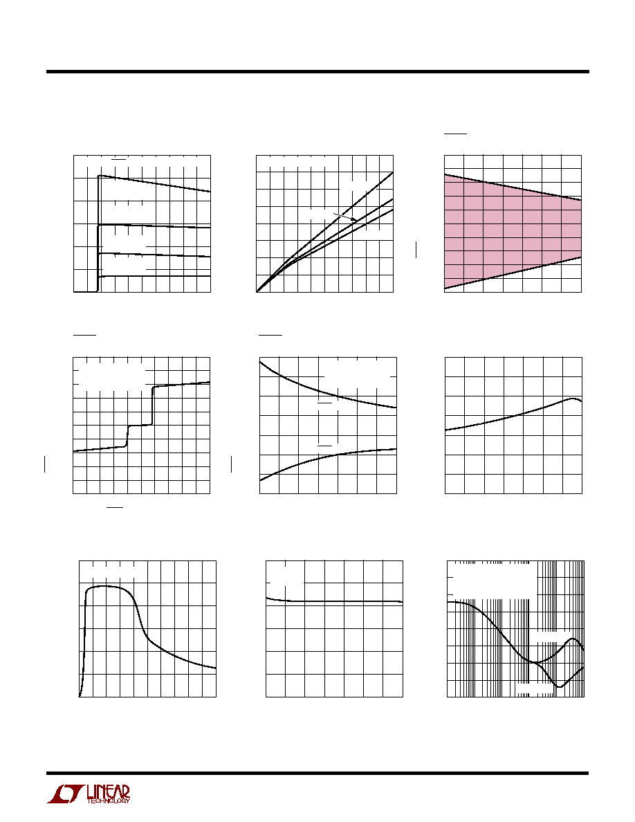
Typical Dropout Voltage
Guaranteed Dropout Voltage
Dropout Voltage
Quiescent Current
LT1964-5 Output Voltage
LT1964-BYP, LT1964-SD
ADJ Pin Voltage
LT1964-5
Quiescent Current
LT1964-BYP, LT1964-SD
Quiescent Current
LT1964-5
GND Pin Current
LT1964
5
1964f
TYPICAL PERFOR A CE CHARACTERISTICS
U
W
3.0
2.5
2.0
1.5
1.0
0.5
0
1964 G10
GND PIN CURRENT (mA)
0
1 2 3 4 5 6 7 8 9 10
R
L
= 12.2
I
L
= 100mA*
R
L
= 24.4
I
L
= 50mA*
R
L
= 122
I
L
= 10mA*
T
J
= 25
°
C; V
SHDN
= V
IN
; *FOR V
OUT
= 1.22V
R
L
= 6.1
I
L
= 200mA*
INPUT VOLTAGE (V)
4.0
3.5
3.0
2.5
2.0
1.5
1.0
0.5
0
1964 G11
GND PIN CURRENT (mA)
0
40
80
120
160
200
V
IN
= V
OUT(NOMINAL)
1V
T
J
= 50
°
C
T
J
= 25
°
C
T
J
= 125
°
C
OUTPUT CURRENT (mA)
2.5
2.0
1.5
1.0
0.5
0
0.5
1.0
1.5
2.0
2.5
1964 G12
SHDN PIN VOLTAGE (V)
ON
ON
OFF
TEMPERATURE (
°
C)
50
25
0
25
50
75
100
125
10
8
6
4
2
0
2
4
6
8
10
1964 G13
SHDN PIN INPUT CURRENT (
µ
A)
SHDN PIN VOLTAGE (V)
10 8 6 4 2
0
2
4
6
8
10
T
J
= 25
°
C
POSITIVE CURRENT
FLOWS INTO THE PIN
12
9
6
3
0
3
6
9
1964 G14
SHDN PIN INPUT CURRENT (
µ
A)
TEMPERATURE (
°
C)
50
25
0
25
50
75
100
125
V
SHDN
= 15V
V
SHDN
= 15V
V
IN
= 15V
POSITIVE CURRENT
FLOWS INTO THE PIN
70
60
50
40
30
20
10
0
1964 G15
ADJ PIN BIAS CURRENT (nA)
TEMPERATURE (
°
C)
50
25
0
25
50
75
100
125
INPUT/OUTPUT DIFFERENTIAL (V)
0
600
500
400
300
200
100
0
1964 G16
4
8
12
16
20
CURRENT LIMIT (mA)
V
OUT
= 100mV
TEMPERATURE (
°
C)
600
500
400
300
200
100
0
1964 G17
CURRENT LIMIT (mA)
50
25
0
25
50
75
100
125
V
IN
= 7V
V
OUT
= 0V
10
100
1k
10k
100k
1M
FREQUENCY (Hz)
RIPPLE REJECTION (dB)
80
70
60
50
40
30
20
10
0
1964 G18
I
L
= 200mA
V
IN
= V
OUT(NOMINAL)
1V +
50mV
RMS
RIPPLE
C
BYP
= 0
C
OUT
= 10
µ
F
C
OUT
= 1
µ
F
LT1964-BYP, LT1964-SD
GND Pin Current
GND Pin Current vs I
LOAD
SHDN Pin Thresholds
SHDN Pin Input Current
SHDN Pin Input Current
ADJ Pin Bias Current
Current Limit
Current Limit
Input Ripple Rejection