 | ÐлекÑÑоннÑй компоненÑ: LT1969 | СкаÑаÑÑ:  PDF PDF  ZIP ZIP |
Äîêóìåíòàöèÿ è îïèñàíèÿ www.docs.chipfind.ru
1
LT1969
Dual 700MHz, 200mA,
Adjustable Current Operational Amplifier
s
700MHz Gain Bandwidth
s
±
200mA Minimum I
OUT
s
Adjustable Quiescent Current
s
Low Distortion: 72dBc at 1MHz, 4V
P-P
, 25
, A
V
= 2
s
Stable in A
V
10, Simple Compensation for A
V
< 10
s
±
4.3V Minimum Output Swing, V
S
=
±
6V, R
L
= 25
s
Stable with 1000pF Load
s
6nV/
Hz Input Noise Voltage
s
2pA/
Hz Input Noise Current
s
4mV Maximum Input Offset Voltage
s
4
µ
A Maximum Input Bias Current
s
400nA Maximum Input Offset Current
s
±
4.5V Minimum Input CMR, V
S
=
±
6V
s
Specified at
±
6V,
±
2.5V
The LT
®
1969 is an adjustable current version of the
popular LT1886, a 200mA minimum output current, dual
op amp with outstanding distortion performance. The
adjustable current feature is highly desirable in applica-
tions where minimum power dissipation is required while
still being able to provide adequate line termination.
At nominal supply current, the amplifiers are gain of 10
stable and can easily be compensated for lower gains. The
LT1969 features balanced high impedance inputs with
4
µ
A input bias current and 4mV maximum input offset
voltage. Single supply applications are easy to implement
and have lower total noise than current feedback amplifier
implementations.
The output drives a 25
load to
±
4.3V with
±
6V supplies.
On
±
2.5V supplies, the output swings
±
1.5V with a 100
load. The amplifier is stable with a 1000pF capacitive load
making it useful in buffer and cable driver applications.
The LT1969 is manufactured on Linear Technology's
advanced low voltage complementary bipolar process and
is available in a thermally enhanced MS10 package
s
DSL Modems
s
xDSL PCI Cards
s
USB Modems
s
Line Drivers
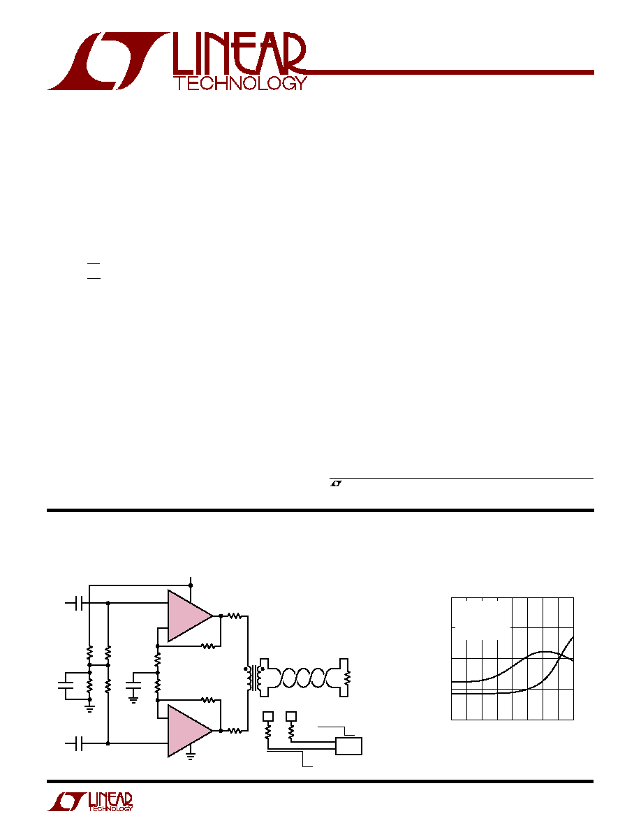
Single 12V Supply ADSL Modem Line Driver
ADSL Modem Line Driver Distortion
, LTC and LT are registered trademarks of Linear Technology Corporation.
+
1/2 LT1969
12.4
1:2*
12V
909
100
100
20k
10k
IN
IN
+
10k
20k
1
µ
F
1
µ
F
0.1
µ
F
0.1
µ
F
+
1/2 LT1969
12.4
1969 TA01a
909
100
13k
*COILCRAFT X8390-A
OR EQUIVALENT
6
49.9k
STANDBY ON
I
Q
ON = 14mA
I
Q
LOW POWER = 2mA
I
Q
STANDBY = 600
µ
A
LOGIC
OUTPUT
CTRL1 CTRL2
7
STANDBY
LOW POWER ON
LINE VOLTAGE (V
P-P
)
0
HARMONIC DISTORTION (dBc)
60
70
80
90
100
1969 TA01b
2
4
6
8
10
12
14
16
V
S
= 12V
A
V
= 10
f = 200kHz
100
LINE
1:2 TRANSFORMER
HD2
HD3
FEATURES
DESCRIPTIO
U
APPLICATIO S
U
TYPICAL APPLICATIO
U
2
LT1969
W
U
U
PACKAGE/ORDER I FOR ATIO
LT1969CMS
T
JMAX
= 150
°
C,
JA
= 110
°
C/W (NOTE 4)
ORDER PART
NUMBER
ELECTRICAL CHARACTERISTICS
The
q
denotes specifications which apply over the full operating temp-
erature range, otherwise specifications are at T
A
= 25
°
C. V
S
=
±
6V, V
CM
= 0V, nominal mode with a 13k resistor from CTRL1 to V
and
a 49.9k resistor from CTRL2 to V
, pulse power tested unless otherwise noted. (Note 9)
SYMBOL
PARAMETER
CONDITIONS
MIN
TYP
MAX
UNITS
V
OS
Input Offset Voltage
(Note 5)
1
4
mV
q
5
mV
Input Offset Voltage Drift
(Note 8)
q
3
17
µ
V/
°
C
I
OS
Input Offset Current
150
400
nA
q
600
nA
I
B
Input Bias Current
1.5
4
µ
A
q
6
µ
A
e
n
Input Noise Voltage
f = 10kHz
6
nV/
Hz
i
n
Input Noise Current
f = 10kHz
2
pA/
Hz
R
IN
Input Resistance
V
CM
=
±
4.5V
5
10
M
Differential
35
k
C
IN
Input Capacitance
2
pF
Input Voltage Range (Positive)
q
4.5
5.9
V
Input Voltage Range (Negative)
q
5.2
4.5
V
CMRR
Common Mode Rejection Ratio
V
CM
=
±
4.5V
q
77
98
dB
Minimum Supply Voltage
Guaranteed by PSRR
q
±
2
V
PSRR
Power Supply Rejection Ratio
V
S
=
±
2V to
±
6.5V
80
86
dB
q
78
dB
A
VOL
Large-Signal Voltage Gain
V
OUT
=
±
4V, R
L
= 100
5.0
12
V/mV
q
4.5
V/mV
V
OUT
=
±
4V, R
L
= 25
4.5
12
V/mV
q
4.0
V/mV
V
OUT
Output Swing
R
L
= 100
, 10mV Overdrive
4.85
5
±
V
q
4.70
±
V
R
L
= 25
, 10mV Overdrive
4.30
4.6
±
V
q
4.10
±
V
I
OUT
= 200mA, 10mV Overdrive
4.30
4.5
±
V
q
4.10
±
V
MS10 PART MARKING
LTTN
ABSOLUTE
M
AXI
M
U
M
RATINGS
W
W
W
U
(Note 1)
Total Supply Voltage (V
+
to V
) ........................... 13.2V
Input Current (Note 2) .......................................
±
10mA
Input Voltage (Note 2) ............................................
±
V
S
Maximum Continuous Output Current (Note 3)
DC ...............................................................
±
100mA
AC ...............................................................
±
300mA
Operating Temperature Range (Note 10) 40
°
C to 85
°
C
Specified Temperature Range (Note 9) .. 40
°
C to 85
°
C
Maximum Junction Temperature ......................... 150
°
C
Storage Temperature Range ................ 65
°
C to 150
°
C
Lead Temperature (Soldering, 10 sec)................. 300
°
C
Consult factory for parts specified with wider operating temperature ranges.
1
2
3
4
5
V
+
OUTA
INA
+INA
V
10
9
8
7
6
OUTB
INB
+INB
CTRL2
CTRL1
TOP VIEW
MS10 PACKAGE
10-LEAD PLASTIC MSOP
3
LT1969
ELECTRICAL CHARACTERISTICS
The
q
denotes specifications which apply over the full operating temp-
erature range, otherwise specifications are at T
A
= 25
°
C. V
S
=
±
6V, V
CM
= 0V, nominal mode with a 13k resistor from CTRL1 to V
and
a 49.9k resistor from CTRL2 to V
, pulse power tested unless otherwise noted. (Note 9)
SYMBOL
PARAMETER
CONDITIONS
MIN
TYP
MAX
UNITS
I
SC
Short-Circuit Current (Sourcing)
(Note 3)
700
mA
Short-Circuit Current (Sinking)
500
mA
SR
Slew Rate
A
V
= 10 (Note 6)
100
200
V/
µ
s
Full Power Bandwidth
4V Peak (Note 7)
8
MHz
GBW
Gain Bandwidth
f = 1MHz
700
MHz
t
r
, t
f
Rise Time, Fall Time
A
V
= 10, 10% to 90% of 0.1V, R
L
= 100
4
ns
Overshoot
A
V
= 10, 0.1V, R
L
= 100
1
%
Propagation Delay
A
V
= 10, 50% V
IN
to 50% V
OUT
, 0.1V, R
L
= 100
2.5
ns
t
S
Settling Time
6V Step, 0.1%
50
ns
Harmonic Distortion
HD2, A
V
= 10, 2V
P-P
, f = 1MHz, R
L
= 100
/25
75/63
dBc
HD3, A
V
= 10, 2V
P-P
, f = 1MHz, R
L
= 100
/25
85/71
dBc
IMD
Intermodulation Distortion
A
V
= 10, f = 0.9MHz, 1MHz, 14dBm, R
L
= 100
/25
81/80
dBc
R
OUT
Output Resistance
A
V
= 10, f = 1MHz
0.1
I
S
Supply Current
Per Amplifier
7
8.25
mA
q
8.50
mA
CTRL1 Voltage
13k to V
, Measured with Respect to V
0.77
0.97
1.25
V
q
0.74
1.30
V
CTRL2 Voltage
49.9k to V
, Measured with Respect to V
0.87
1.05
1.18
V
q
0.80
1.25
V
Minimum Supply Current
per Amplifier; CTRL1, CTRL2 Open
300
800
µ
A
q
1100
µ
A
Maximum Supply Current
per Amplifier; CTRL1 or CTRL2 Shorted to V
13
mA
The
q
denotes specifications which apply over the full operating temperature range, otherwise specifications are at T
A
= 25
°
C.
V
S
=
±
2.5V, V
CM
= 0V, nominal mode with a 13k resistor from CTRL1 to V
and a 49.9k resistor from CTRL2 to V
, pulse power tested
unless otherwise noted. (Note 9)
SYMBOL
PARAMETER
CONDITIONS
MIN
TYP
MAX
UNITS
V
OS
Input Offset Voltage
(Note 5)
1.5
5
mV
q
6
mV
Input Offset Voltage Drift
(Note 8)
q
5
17
µ
V/
°
C
I
OS
Input Offset Current
100
350
nA
q
550
nA
I
B
Input Bias Current
1.2
3.5
µ
A
q
5.5
µ
A
e
n
Input Noise Voltage
f = 10kHz
6
nV/
Hz
i
n
Input Noise Current
f = 10kHz
2
pA/
Hz
R
IN
Input Resistance
V
CM
=
±
1V
10
20
M
Differential
50
k
C
IN
Input Capacitance
2
pF
Input Voltage Range (Positive)
q
1
2.4
V
Input Voltage Range (Negative)
q
1.7
1
V
CMRR
Common Mode Rejection Ratio
V
CM
=
±
1V
q
75
91
dB
4
LT1969
ELECTRICAL CHARACTERISTICS
The
q
denotes specifications which apply over the full operating temp-
erature range, otherwise specifications are at T
A
= 25
°
C. V
S
=
±
2.5V, V
CM
= 0V, nominal mode with a 13k resistor from CTRL1 to V
and a 49.9k resistor from CTRL2 to V
, pulse power tested unless otherwise noted. (Note 9)
SYMBOL
PARAMETER
CONDITIONS
MIN
TYP
MAX
UNITS
Note 1: Absolute Maximum Ratings are those values beyond which the life
of a device may be impaired.
Note 2: The inputs are protected by back-to-back diodes. If the differential
input voltage exceeds 0.7V, the input current should be limited to less than
10mA.
Note 3: A heat sink may be required to keep the junction temperature
below absolute maximum.
Note 4: Thermal resistance varies depending upon the amount of PC board
metal attached to the device.
JA
is specified for a 2500mm
2
test board
covered with 2 oz copper on both sides.
Note 5: Input offset voltage is exclusive of warm-up drift.
Note 6: Slew rate is measured between
±
2V on a
±
4V output with
±
6V
supplies, and between
±
1V on a
±
1.5V output with
±
2.5V supplies. Falling
slew rate is guaranteed by correlation to rising slew rate.
Note 7: Full power bandwidth is calculated from the slew rate:
FPBW = SR/2
V
P
.
Note 8: This parameter is not 100% tested.
Note 9: The LT1969C is guaranteed to meet specified performance from 0
°
C
to 70
°
C. The LT1969C is designed, characterized and expected to meet
specified performance from 40
°
C to 85
°
C but is not tested or QA sampled
at these temperatures.
Note 10: The LT1969C is guaranteed functional over the operating temperature
range of 40
°
C to 85
°
C.
A
VOL
Large-Signal Voltage Gain
V
OUT
=
±
1V, R
L
= 100
5.0
10
V/mV
q
4.5
V/mV
V
OUT
=
±
1V, R
L
= 25
4.5
10
V/mV
q
4.0
V/mV
V
OUT
Output Swing
R
L
= 100
, 10mV Overdrive
1.50
1.65
±
V
q
1.40
±
V
R
L
= 25
, 10mV Overdrive
1.35
1.50
±
V
q
1.25
±
V
I
OUT
= 200mA, 10mV Overdrive
0.87
1
±
V
q
0.80
±
V
I
SC
Short-Circuit Current (Sourcing)
(Note 3)
500
mA
Short-Circuit Current (Sinking)
400
mA
SR
Slew Rate
A
V
= 10 (Note 6)
50
100
V/
µ
s
Full Power Bandwidth
1V Peak (Note 7)
16
MHz
GBW
Gain Bandwidth
f = 1MHz
530
MHz
t
r
, t
f
Rise Time, Fall Time
A
V
= 10, 10% to 90% of 0.1V, R
L
= 100
7
ns
Overshoot
A
V
= 10, 0.1V, R
L
= 100
5
%
Propagation Delay
A
V
= 10, 50% V
IN
to 50% V
OUT
, 0.1V, R
L
= 100
5
ns
Harmonic Distortion
HD2, A
V
= 10, 2V
P-P
, f = 1MHz, R
L
= 100
/25
75/ 64
dBc
HD3, A
V
= 10, 2V
P-P
, f = 1MHz, R
L
= 100
/25
80/ 66
dBc
IMD
Intermodulation Distortion
A
V
= 10, f = 0.9MHz, 1MHz, 5dBm, R
L
= 100
/25
77/ 85
dBc
R
OUT
Output Resistance
A
V
= 10, f = 1MHz
0.2
Channel Separation
V
OUT
=
±
1V, R
L
= 25
82
92
dB
q
80
dB
I
S
Supply Current
Per Amplifier
5
6.00
mA
q
6.25
mA
CTRL1 Voltage
13k to V
, Measured with Respect to V
0.77
0.95
1.25
V
q
0.74
1.30
V
CTRL2 Voltage
49.9k to V
, Measured with Respect to V
0.87
1.03
1.18
V
q
0.80
1.25
V
Minimum Supply Current
per Amplifier; CTRL1, CTRL2 Open
250
650
µ
A
q
750
µ
A
Maximum Supply Current
per Amplifier; CTRL1 or CTRL2 Shorted to V
11.5
mA
5
LT1969
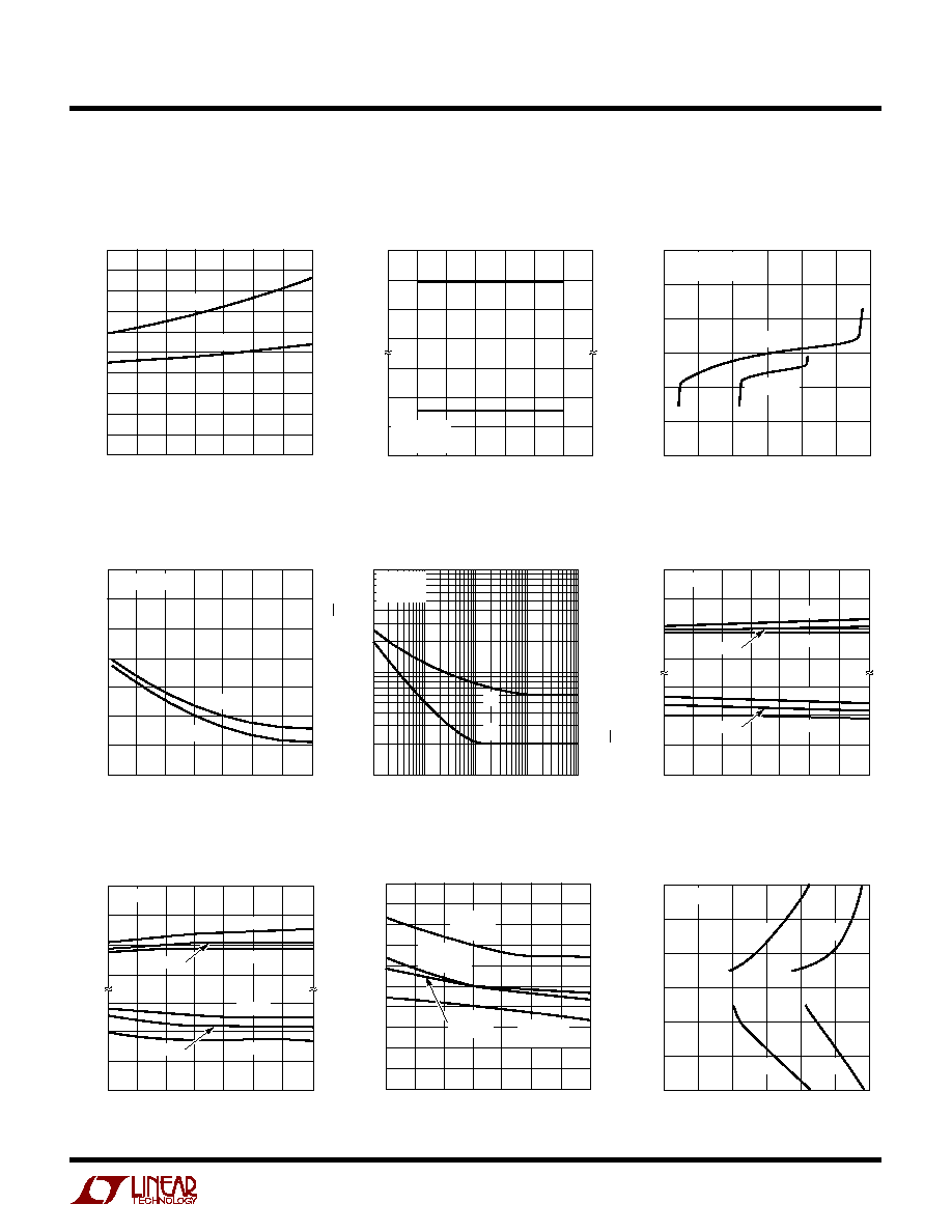
Input Noise Spectral Density
TYPICAL PERFOR A CE CHARACTERISTICS
U
W
Supply Current vs Temperature
Input Common Mode Range
vs Supply Voltage
Input Bias Current
vs Input Common Mode Voltage
13k resistor from CTRL1 to V
and a 49.9k resistor from CTRL2 to V
TOTAL SUPPLY VOLTAGE (V)
0
2
4
6
8
10
12
14
COMMON MODE RANGE (V)
1969 G02
V
+
0.1
0.2
0.3
1.5
1.0
0.5
V
T
A
= 25
°
C
V
OS
> 1mV
INPUT COMMON MODE VOLTAGE (V)
6
2
2
4
0
4
6
INPUT BIAS CURRENT (
µ
A)
1969 G03
3.0
2.5
2.0
1.5
1.0
0.5
0
T
A
= 25
°
C
I
B
= (I
B+
+ I
B
)/2
V
S
=
±
6V
V
S
=
±
2.5V
FREQUENCY (Hz)
10
1
INPUT VOLTAGE NOISE (nV/
Hz)
10
100
INPUT CURRENT NOISE (pA/
Hz)
10
1
100
1k
100k
100
10k
1969 G04
e
n
T
A
= 25
°
C
A
V
= 101
i
n
TEMPERATURE (
°
C)
50
0
SUPPLY CURRENT, BOTH AMPLIFIERS (mA)
2
6
8
10
20
14
0
50
75
1969 G01
4
16
18
12
25
25
100
125
V
S
=
±
6V
V
S
=
±
2.5V
Input Bias Current
vs Temperature
TEMPERATURE (
°
C)
50
2.0
2.5
3.5
25
75
1969 G43
1.5
1.0
25
0
50
100
125
0.5
0
3.0
INPUT BIAS CURRENT (
µ
A)
I
B
= (I
B
+
I
B
)/2
V
S
=
±
6V
V
S
=
±
2.5V
Output Saturation Voltage
vs Temperature
TEMPERATURE (
°
C)
50
1.5
1.0
V
+
25
75
1969 G44
1.5
1.0
25
0
50
100
125
0.5
V
0.5
OUTPUT SATURATION VOLTAGE (V)
200mA
200mA
150mA
R
L
= 100
R
L
= 100
V
S
=
±
6V
150mA
Output Saturation Voltage
vs Temperature
TEMPERATURE (
°
C)
50
1.5
1.0
V
+
25
75
1969 G45
1.5
1.0
25
0
50
100
125
0.5
V
0.5
OUTPUT SATURATION VOLTAGE (V)
200mA
200mA
150mA
R
L
= 100
R
L
= 100
V
S
=
±
2.5V
150mA
Settling Time vs Output Step
SETTLING TIME (ns)
0
20
40
10
30
50
60
OUTPUT STEP (V)
1886 G05
6
4
2
0
2
4
6
V
S
=
±
6V
10mV
1mV
10mV
1mV
Output Short-Circuit Current
vs Temperature
TEMPERATURE (
°
C)
50
0
OUTPUT SHORT-CIRCUIT CURRENT (mA)
100
300
400
500
1000
700
0
50
75
1969 G46
200
800
900
600
25
25
100
125
SOURCE
V
S
=
±
6V
SOURCE
V
S
=
±
2.5V
SINK
V
S
=
±
2.5V
SINK
V
S
=
±
6V