 | ÐлекÑÑоннÑй компоненÑ: LT2179 | СкаÑаÑÑ:  PDF PDF  ZIP ZIP |
Äîêóìåíòàöèÿ è îïèñàíèÿ www.docs.chipfind.ru
1
LT 2178/LT 2179
17
µ
A Max, Dual and Quad,
Single Supply, Precision Op Amps
FEATURES
s
SO Package with Standard Pinout
s
Supply Current per Amplifier: 17
µ
A Max
s
Offset Voltage: 70
µ
V Max
s
Offset Current: 250pA Max
s
Input Bias Current: 5nA Max
s
Voltage Noise: 0.9
µ
V
P-P
, 0.1Hz to 10Hz
s
Current Noise: 1.5pA
P-P
, 0.1Hz to 10Hz
s
Offset Voltage Drift: 0.5
µ
V/
°
C
s
Gain Bandwidth Product: 85kHz
s
Slew Rate: 0.04V/
µ
s
s
Single Supply Operation
Input Voltage Range Includes Ground
Output Swings to Ground while Sinking Current
No Pull-Down Resistors Needed
s
Output Sources and Sinks 5mA Load Current
DESCRIPTIO
N
U
The LT
®
2178 is a micropower dual op amp in a surface
mount standard 8-pin configuration, the LT2179 is a
micropower quad op amp offered in a surface mount 14-pin
package. Both devices are optimized for single supply opera-
tion at 5V. Specifications are also provided at
±
15V supply.
The extremely low supply current is combined with true
precision specifications: offset voltage is 30
µ
V and offset
current is 50pA. Both offset parameters have low drift
with temperature. The 1.5pA
P-P
current noise and
picoampere offset current permit the use the megohm
level source resistors without introducing serious errors.
Voltage noise, at 0.9
µ
V
P-P
, is remarkably low considering
the low supply current.
The LT2178/LT2179 can be operated from a single supply
(as low as one lithium-cell or two NiCd batteries). The input
range goes below ground. The all-NPN output stage swings
to within a few millivolts of ground while sinking current. No
power consuming pull down resistors are needed.
For surface mount applications where three times higher
supply current is acceptable, the micropower LT1077
single, LT2078 dual and LT2079 quad are recommended.
The LT1077/LT2078/LT2079 have significantly higher
bandwidth, slew rate, lower voltage noise and better
output drive capability. For applications requiring DIP
packages refer to the LT1178/LT1179.
s
Battery- or Solar-Powered Systems
Portable Instrumentation
Remote Sensor Amplifier
Satellite Circuitry
s
Micropower Sample-and-Hold
s
Thermocouple Amplifier
s
Micropower Filters
APPLICATIO
N
S
U
, LTC and LT are registered trademarks of Linear Technology Corporation.
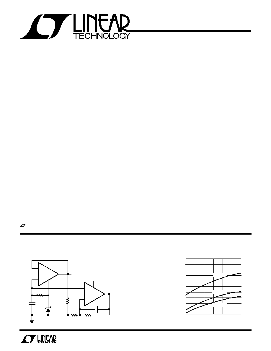
TYPICAL APPLICATIO
N
U
Self-Buffered, Dual Output, Micropower Reference
Supply Current vs Temperature
+
2
3
+
5
6
1/2 LT2178
1
0.1
µ
F
250k
1M*
1M*
LT1004-1.2
4
7
2M
0.1
µ
F
1.2365V
OUTPUT
1/2 LT2178
2.470V
OUTPUT
4V TO 9V
LT2178/79 · TA01
TOTAL BATTERY CURRENT = 28
µ
A
OUTPUT ACCURACY =
±
0.4% MAX
TEMPERATURE COEFFICIENT = 20ppm/
°
C
LOAD REGULATION = 25ppm/mA, I
L
5mA, V
+
5V
LINE REGULATION = 10ppm/V
* 0.1% FILM RESISTORS
8
TEMPERATURE (
°
C)
50
SUPPLY CURRENT PER AMPLIFIER (
µ
A)
25
0
25
50
LT2178/79 · TPC02
75
20
18
16
14
12
10
100
V
S
=
±
15V
V
S
= 5V, 0V
V
S
=
±
1.5V
2
LT2178/LT 2179
ABSOLUTE
M
AXI
M
U
M
RATINGS
W
W
W
U
Supply Voltage ......................................................
±
22V
Differential Input Voltage .......................................
±
30V
Input Voltage ............... Equal to Positive Supply Voltage
............ 5V Below Negative Supply Voltage
Output Short-Circuit Duration .......................... Indefinite
Specified Temperature Range
Commercial ............................................. 0
°
C to 70
°
C
Industrial ............................................ 40
°
C to 85
°
C
Storage Temperature Range ................. 65
°
C to 150
°
C
Lead Temperature (Soldering, 10 sec).................. 300
°
C
T
JMAX
= 150
°
C,
JA
= 150
°
C/ W
T
JMAX
= 150
°
C,
JA
= 190
°
C/ W
Consult factory for Military grade parts.
V
S
= 5V, 0V, V
CM
= 0.1V, V
O
= 1.4V, T
A
= 25
°
C, unless otherwise noted.
LT2178AC/LT2178AI
LT2178C/LT2178I
LT2179AC/LT2179AI
LT2179C/LT2179I
SYMBOL
PARAMETER
CONDITIONS (NOTE 1)
MIN
TYP
MAX
MIN
TYP
MAX
UNITS
V
OS
Input Offset Voltage
LT2178
30
70
40
120
µ
V
LT2179
35
100
40
150
µ
V
V
OS
Long Term Input Offset
0.5
0.6
µ
V/Mo
Time
Voltage Stability
I
OS
Input Offset Current
0.05
0.25
0.05
0.35
nA
I
B
Input Bias Current
3
5
3
6
nA
e
n
Input Noise Voltage
0.1Hz to 10Hz (Note 2)
0.9
2.0
0.9
µ
V
P-P
Input Noise Voltage Density
f
O
= 10Hz (Note 2)
50
75
50
nV
Hz
f
O
= 1000Hz (Note 2)
49
65
49
nV
Hz
i
n
Input Noise Current
0.1Hz to 10Hz (Note 2)
1.5
2.5
1.5
pA
P-P
Input Noise Current Density
f
O
= 10Hz (Note 2)
0.03
0.07
0.03
pA
Hz
f
O
= 1000Hz
0.01
0.01
pA
Hz
Input Resistance
(Note 3)
Differential Mode
0.8
2.0
0.6
2.0
G
Common Mode
12
12
G
Input Voltage Range
3.5
3.9
3.5
3.9
V
0
0.3
0
0.3
V
CMRR
Common Mode Rejection Ratio
V
CM
= 0V to 3.5V
93
103
90
102
dB
PSRR
Power Supply Rejection Ratio
V
S
= 2.2V to 12V
94
104
92
104
dB
ELECTRICAL CHARACTERISTICS
ORDER PART
NUMBER
LT2178ACS8
LT2178AIS8
LT2178CS8
LT2178IS8
2178A
2178AI
2178
2178I
PART MARKING
PACKAGE/ORDER I
N
FOR
M
ATIO
N
W
U
U
ORDER PART
NUMBER
LT2179ACS
LT2179AIS
LT2179CS
LT2179IS
1
2
3
4
8
7
6
5
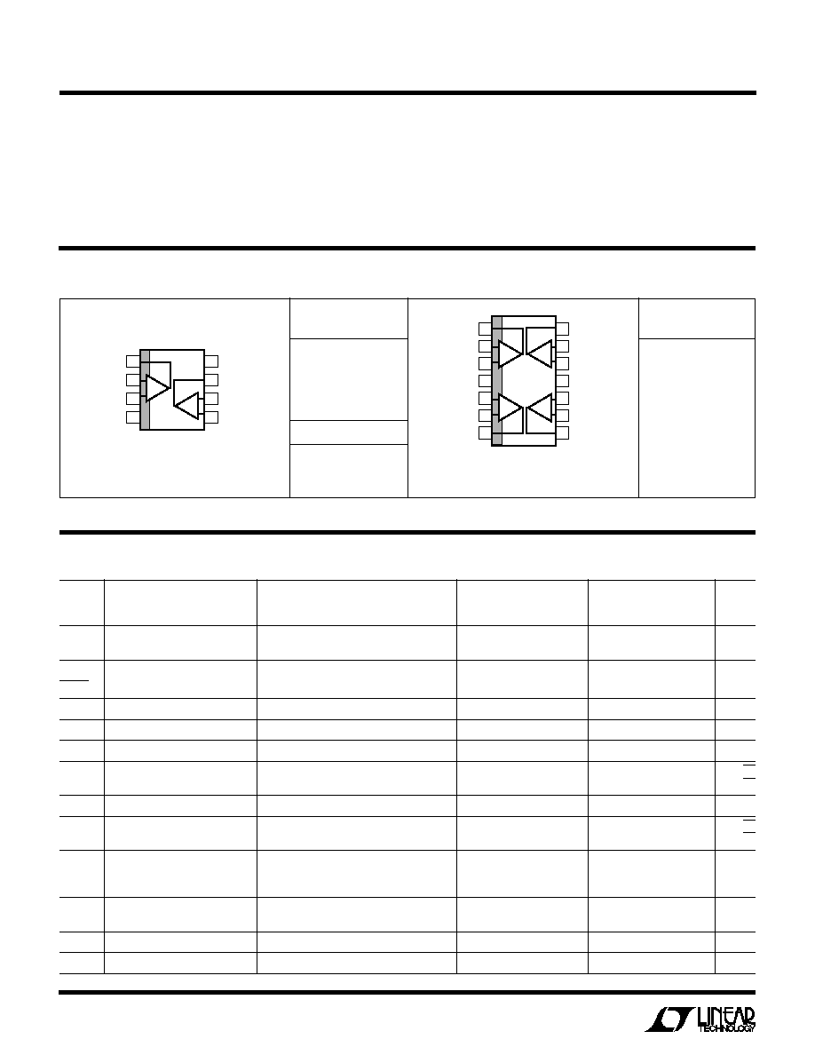
TOP VIEW
V
+
OUT B
IN B
+IN B
OUT A
IN A
+IN A
V
S8 PACKAGE
8-LEAD PLASTIC SO
+
A
+
B
TOP VIEW
S PACKAGE
14-LEAD PLASTIC SO
1
2
3
4
5
6
7
14
13
12
11
10
9
8
OUT A
IN A
+IN A
V
+
+IN B
IN B
OUT B
OUT D
IN D
+IN D
V
+IN C
IN C
OUT C
+
A
+
+
+
D
B
C
3
LT 2178/LT 2179
ELECTRICAL CHARACTERISTICS
V
S
= 5V, 0V, V
CM
= 0.1V, V
O
= 1.4V, T
A
= 25
°
C, unless otherwise noted.
LT2178AC/LT2178AI
LT2178C/LT2178I
LT2179AC/LT2179AI
LT2179C/LT2179I
SYMBOL
PARAMETER
CONDITIONS (NOTE 1)
MIN
TYP
MAX
MIN
TYP
MAX
UNITS
A
VOL
Large-Signal Voltage Gain
V
O
= 0.03V to 4V, No Load (Note 3)
140
700
110
700
V/mV
V
O
= 0.03V to 3.5V, R
L
= 50k
80
200
70
200
V/mV
Maximum Output Voltage
Output Low, No Load
6.5
9
6.5
9
mV
Swing
Output Low, 2k to GND
0.2
0.6
0.2
0.6
mV
Output Low, I
SINK
= 100
µ
A
120
160
120
160
mV
Output High, No Load
4.2
4.4
4.2
4.4
V
Output High, 2k to GND
3.5
3.8
3.5
3.8
V
SR
Slew Rate
A
V
= 1, C
L
= 10pF (Note 3)
0.013
0.025
0.013
0.025
V/
µ
s
GBW
Gain Bandwidth Product
f
O
5kHz
60
60
kHz
I
S
Supply Current per Amplifier
13
18
14
21
µ
A
V
S
=
±
1.5V, V
O
= 0V
12
17
13
20
µ
A
Channel Separation
V
IN
= 3V, R
L
= 10k
110
110
dB
Minimum Supply Voltage
(Note 4)
2.0
2.2
2.0
2.2
V
V
S
= 5V, 0V, V
CM
= 0.1V, V
O
= 1.4V, 40
°
C
T
A
85
°
C for I grades, unless otherwise noted. (Note 6)
LT2178AI/LT2179AI
LT2178I/LT2179I
SYMBOL
PARAMETER
CONDITIONS
MIN
TYP
MAX
MIN
TYP
MAX
UNITS
V
OS
Input Offset Voltage
LT2178
q
70
270
95
370
µ
V
LT2179
q
80
300
100
400
µ
V
V
OS
Input Offset Voltage Drift
LT2178 (Note 5)
q
0.4
1.8
0.5
2.5
µ
V/
°
C
T
LT2179
0.5
3.0
0.6
3.5
µ
V/
°
C
I
OS
Input Offset Current
q
0.07
0.70
0.1
1.0
nA
I
B
Input Bias Current
q
3
7
4
8
nA
CMRR
Common Mode Rejection Ratio
V
CM
= 0.05V to 3.2V
q
86
100
84
98
dB
PSRR
Power Supply Rejection Ratio
V
S
= 3V to 12V
q
88
100
86
100
dB
A
VOL
Large-Signal Voltage Gain
V
O
= 0.05V to 4V, No Load (Note 3)
q
75
350
50
350
V/mV
V
O
= 0.05V to 3.5V, R
L
= 50k
q
40
130
30
130
V/mV
Maximum Output Voltage
Output Low, No Load
q
9
13
9
13
mV
Swing
Output Low, I
SINK
= 100
µ
A
q
160
220
160
220
mV
Output High, No Load
q
3.9
4.2
3.9
4.2
V
Output High, 2k to GND
q
3.0
3.7
3.0
3.7
V
I
S
Supply Current per Amplifier
q
15
24
15
27
µ
A
LT2178AC/LT2179AC
LT2178C/LT2179C
SYMBOL
PARAMETER
CONDITIONS
MIN
TYP
MAX
MIN
TYP
MAX
UNITS
V
OS
Input Offset Voltage
LT2178
q
50
170
65
250
µ
V
LT2179
q
60
200
70
290
µ
V
V
OS
Input Offset Voltage Drift
LT2178 (Note 5)
q
0.4
1.8
0.5
2.5
µ
V/
°
C
T
LT2179
0.5
3.0
0.6
3.5
µ
V/
°
C
I
OS
Input Offset Current
q
0.06
0.35
0.06
0.50
nA
I
B
Input Bias Current
q
3
6
3
7
nA
CMRR
Common Mode Rejection Ratio
V
CM
= 0V to 3.4V
q
90
101
86
100
dB
PSRR
Power Supply Rejection Ratio
V
S
= 2.5V to 12V
q
90
102
88
102
dB
V
S
= 5V, 0V, V
CM
= 0.1V, V
O
= 1.4V, 0
°
C
T
A
70
°
C, unless otherwise noted. (Note 7)
4
LT2178/LT 2179
ELECTRICAL CHARACTERISTICS
LT2178AC/LT2179AC
LT2178C/LT2179C
SYMBOL
PARAMETER
CONDITIONS
MIN
TYP
MAX
MIN
TYP
MAX
UNITS
A
VOL
Large-Signal Voltage Gain
V
O
= 0.05V to 4V, No Load (Note 3)
q
150
500
80
500
V/mV
V
O
= 0.05V to 3.5V, R
L
= 50k
q
55
160
45
160
V/mV
Maximum Output Voltage
Output Low, No Load
q
8
11
8
11
mV
Swing
Output Low, I
SINK
= 100
µ
A
q
140
190
140
190
mV
Output High, No Load
q
4.1
4.3
4.1
4.3
V
Output High, 2k to GND
q
3.3
3.8
3.3
3.8
V
I
S
Supply Current per Amplifier
q
14
21
15
24
µ
A
V
S
= 5V, 0V, V
CM
= 0.1V, V
O
= 1.4V, 0
°
C
T
A
70
°
C, unless otherwise noted.
V
S
=
±
15V, T
A
= 25
°
C, unless otherwise noted.
LT2178AC/LT2178AI
LT2178C/LT2178I
LT2179AC/LT2179AI
LT2179C/LT2179I
SYMBOL
PARAMETER
CONDITIONS
MIN
TYP
MAX
MIN
TYP
MAX
UNITS
V
OS
Input Offset Voltage
LT2178
70
300
90
400
µ
V
LT2179
80
350
100
450
µ
V
I
OS
Input Offset Current
0.05
0.25
0.05
0.35
nA
I
B
Input Bias Current
3
5
3
6
nA
Input Voltage Range
13.5
13.9
13.5
13.9
V
15.0
15.3
15.0
15.3
V
CMRR
Common Mode Rejection Ratio
V
CM
= 13.5V to 15V
96
106
93
106
dB
PSRR
Power Supply Rejection Ratio
V
S
= 5V, 0V to
±
18V
96
112
94
112
dB
A
VOL
Large-Signal Voltage Gain
V
O
=
±
10V, R
L
= 50k
300
1200
250
1000
V/mV
V
O
=
±
10V, No Load
600
2500
400
2500
V/mV
V
OUT
Maximum Output Voltage
R
L
= 50k
±
13.0
±
14.2
±
13.0
±
14.2
V
Swing
R
L
= 2k
±
11.0
±
12.7
±
11.0
±
12.7
V
SR
Slew Rate
A
V
= 1
0.02
0.04
0.02
0.04
V/
µ
s
GBW
Gain Bandwidth Product
f
O
5kHz
85
85
kHz
I
S
Supply Current per Amplifier
16
21
17
25
µ
A
V
S
=
±
15V, 40
°
C
T
A
85
°
C for I grades, unless otherwise noted.
LT2178AI/LT2179AI
LT2178I/LT2179I
SYMBOL
PARAMETER
CONDITIONS
MIN
TYP
MAX
MIN
TYP
MAX
UNITS
V
OS
Input Offset Voltage
LT2178
q
100
650
130
740
µ
V
LT2179
q
100
650
130
740
µ
V
V
OS
Input Offset Voltage Drift
LT2178 (Note 5)
q
0.6
1.8
0.7
2.5
µ
V/
°
C
T
LT2179
0.7
3.0
0.9
4.0
µ
V/
°
C
I
OS
Input Offset Current
q
0.07
0.70
0.1
1.0
nA
I
B
Input Bias Current
q
3
7
4
8
nA
A
VOL
Large-Signal Voltage Gain
V
O
=
±
10V, R
L
= 50k
q
150
500
100
500
V/mV
CMRR
Common Mode Rejection Ratio
V
CM
= 13V, 14.9V
q
90
105
88
103
dB
PSRR
Power Supply Rejection Ratio
V
S
= 0V, 5V to
±
18V
q
92
110
88
109
dB
Maximum Output Voltage Swing R
L
= 5k
q
±
11.0
±
13.5
±
11.0
±
13.5
V
I
S
Supply Current per Amplifier
q
18
28
19
30
µ
A
5
LT 2178/LT 2179
ELECTRICAL CHARACTERISTICS
V
S
=
±
15V, 0
°
C
T
A
70
°
C, unless otherwise noted.
LT2178AC/LT2179AC
LT2178C/LT2179C
SYMBOL
PARAMETER
CONDITIONS
MIN
TYP
MAX
MIN
TYP
MAX
UNITS
V
OS
Input Offset Voltage
LT2178
q
100
480
130
660
µ
V
LT2179
q
120
550
150
750
µ
V
V
OS
Input Offset Voltage Drift
LT2178 (Note 5)
q
0.6
1.8
0.7
2.5
µ
V/
°
C
T
LT2179
0.7
3.0
0.9
4.0
µ
V/
°
C
I
OS
Input Offset Current
q
0.06
0.35
0.06
0.35
nA
I
B
Input Bias Current
q
3
6
3
7
nA
A
VOL
Large-Signal Voltage Gain
V
O
=
±
10V, R
L
= 50k
q
200
800
150
750
V/mV
CMRR
Common Mode Rejection Ratio
V
CM
= 13V, 15V
q
94
104
91
104
dB
PSRR
Power Supply Rejection Ratio
V
S
= 5V, 0V to
±
18V
q
93
110
91
110
dB
Maximum Output Voltage Swing
R
L
= 5k
q
±
11.0
±
13.6
±
11.0
±
13.6
V
I
S
Supply Current per Amplifier
q
17
24
18
28
µ
A
The
q
denotes specifications which apply over the full operating
temperature range.
Note 1: Typical parameters are defined as the 60% yield of parameter
distributions of individual amplifiers, i.e., out of 100 LT2179s (or 100
LT2178s) typically 240 op amps (or 120) will be better than the indicated
specification.
Note 2: This parameter is tested on a sample basis only. All noise
parameters are tested with V
S
=
±
2.5V, V
O
= 0V.
Note 3: This parameter is guaranteed by design and is not tested.
Note 4: Power supply rejection ratio is measured at the minimum supply
voltage. The op amps actually work at 1.7V supply but with a typical offset
skew of 300
µ
V.
Note 5: This parameter is not 100% tested.
Note 6: During testing at 40
°
C, the 5V power supply turn-on time is less
than 0.5s.
Note 7: The LT2178C/LT2179C are designed, characterized and expected
to meet the industrial temperature limits, but are not tested at 40
°
C and
85
°
C. I-grade parts are guaranteed.
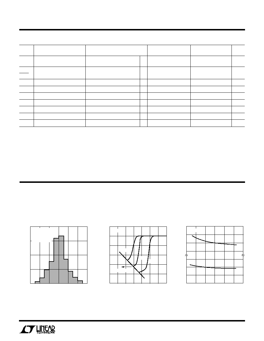
TYPICAL PERFOR
M
A
N
CE CHARACTERISTICS
U
W
Distribution of Input
Offset Voltage
POSITIVE SUPPLY VOLTAGE (V)
0
OFFSET VOLTAGE SHIFT (
µ
V)
100
0
100
200
300
400
500
LT2178/79 · TPC02
1
2
3
V
= 0V
NONFUCTIONAL
40
°
C
25
°
C
85
°
C
TEMPERATURE (
°
C)
50
25
50
75
25
75
LT2178/79 · TPC03
2.5
3.0
25
0
50
100
3.5
4.0
INPUT OFFSET
CURRENT (pA)
INPUT BIAS
CURRENT (nA)
100
I
OS
I
B
V
S
= 5V, 0V
Minimum Supply Voltage
Input Bias and Offset Currents vs
Temperature
OFFSET VOLTAGE (
µ
V)
150
0
NUMBER OF OP AMPS 200
400
600
800
100
50
0
50
LT2178/79 · TPC01
100
150
V
S
= 5V, 0V
T
A
= 25
°
C
2500 OP AMPS
TESTED