
1
LTC1044A
12V CMOS
Voltage Converter
D
U
ESCRIPTIO
S
FEATURE
U
S
A
O
PPLICATI
s
1.5V to 12V Operating Supply Voltage Range
s
13V Absolute Maximum Rating
s
200
µ
A Maximum No Load Supply Current at 5V
s
Boost Pin (Pin 1) for Higher Switching Frequency
s
97% Minimum Open Circuit Voltage Conversion
Efficiency
s
95% Minimum Power Conversion Efficiency
s
I
S
= 1.5
µ
A with 5V Supply When OSC Pin = 0V or V
+
s
High Voltage Upgrade to ICL7660/LTC1044
s
Conversion of 10V to
±
10V Supplies
s
Conversion of 5V to
±
5V Supplies
s
Precise Voltage Division: V
OUT
= V
IN
/2
±
20ppm
s
Voltage Multiplication: V
OUT
=
±
nV
IN
s
Supply Splitter: V
OUT
=
±
V
S
/2
s
Automotive Applications
s
Battery Systems with 9V Wall Adapters/Chargers
The LTC1044A is a monolithic CMOS switched-capacitor
voltage converter. It plugs in for ICL7660/LTC1044 in
applications where higher input voltage (up to 12V) is
needed. The LTC1044A provides several conversion func-
tions without using inductors. The input voltage can be
inverted (V
OUT
= ≠ V
IN
), doubled (V
OUT
= 2V
IN
), divided
(V
OUT
= V
IN
/2) or multiplied (V
OUT
=
±
nV
IN
).
To optimize performance in specific applications, a boost
function is available to raise the internal oscillator fre-
quency by a factor of 7. Smaller external capacitors can be
used in higher frequency operation to save board space.
The internal oscillator can also be disabled to save power.
The supply current drops to 1.5
µ
A at 5V input when the
OSC pin is tied to GND or V
+
.
U
A
O
PPLICATI
TYPICAL
Generating ≠ 10V from 10V
Output Voltage vs Load Current, V
+
= 10V
LOAD CURRENT (mA)
0
OUTPUT VOLTAGE (V)
≠4
≠2
0
40
LTC1044A ∑ TA02
≠6
≠8
≠5
≠3
≠1
≠7
≠9
≠10
10 20 30
50 60 70 80 90 100
T
A
= 25∞C
C1 = C2 = 10
µ
F
SLOPE = 45
1
2
3
4
8
7
6
5
LTC1044A
V
+
OSC
LV
V
OUT
BOOST
CAP
+
GND
CAP
≠
+
10
µ
F
+
10
µ
F
10V INPUT
≠10V OUTPUT
LTC1044A ∑ TA01
2
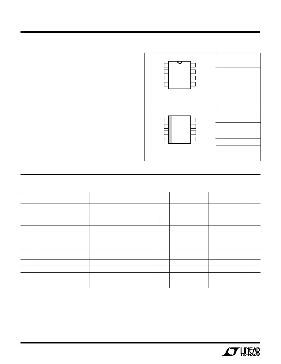
LTC1044A
W
U
U
PACKAGE/ORDER I FOR ATIO
ABSOLUTE AXI U RATI GS
W
W W
U
(Note 1)
Supply Voltage ........................................................ 13V
Input Voltage on Pins 1, 6 and 7
(Note 2) .............................. ≠ 0.3V < V
IN
< V
+
+ 0.3V
Current into Pin 6 ................................................. 20
µ
A
Output Short-Circuit Duration
V
+
6.5V ................................................. Continuous
Operating Temperature Range
LTC1044AC ............................................ 0
∞
C to 70
∞
C
LTC1044AI ........................................ ≠ 40
∞
C to 85
∞
C
Storage Temperature Range ................ ≠ 65
∞
C to 150
∞
C
Lead Temperature (Soldering, 10 sec)................. 300
∞
C
ORDER PART
NUMBER
T
JMAX
= 110
∞
C,
JA
= 100
∞
C/W
ORDER PART
NUMBER
1
2
3
4
8
7
6
5
TOP VIEW
BOOST
CAP
+
GND
CAP
≠
V
+
OSC
LV
V
OUT
N8 PACKAGE
8-LEAD PLASTIC DIP
S8 PART MARKING
LTC1044ACN8
LTC1044AIN8
LTC1044ACS8
LTC1044AIS8
1044A
1044AI
T
JMAX
= 110
∞
C,
JA
= 130
∞
C/W
1
2
3
4
8
7
6
5
TOP VIEW
V
+
OSC
LV
V
OUT
BOOST
CAP
+
GND
CAP
≠
S8 PACKAGE
8-LEAD PLASTIC SOIC
LTC1044AC
LTC1044AI
SYMBOL
PARAMETER
CONDITIONS
MIN
TYP
MAX
MIN
TYP
MAX
UNITS
I
S
Supply Current
R
L
=
, Pins 1 and 7, No Connection
60
200
60
200
µ
A
R
L
=
, Pins 1 and 7, No Connection,
15
15
µ
A
V
+
= 3V
Minimum Supply Voltage
R
L
= 10k
q
1.5
1.5
V
Maximum Supply Voltage
R
L
= 10k
q
12
12
V
R
OUT
Output Resistance
I
L
= 20mA, f
OSC
= 5kHz
100
100
q
120
130
V
+
= 2V, I
L
= 3mA, f
OSC
= 1kHz
q
310
325
f
OSC
Oscillator Frequency
V
+
= 5V, (Note 3)
q
5
5
kHz
V
+
= 2V
q
1
1
kHz
P
EFF
Power Efficiency
R
L
= 5k, f
OSC
= 5kHz
95
98
95
98
%
Voltage Conversion Efficiency
R
L
=
97
99.9
97
99.9
%
Oscillator Sink or Source
V
OSC
= 0V or V
+
Current
Pin 1 (BOOST) = 0V
q
3
3
µ
A
Pin 1 (BOOST) = V
+
q
20
20
µ
A
ELECTRICAL C
C
HARA TERISTICS
V
+
= 5V, C
OSC
= 0pF, T
A
= 25
∞
C, See Test Circuit, unless otherwise noted.
The
q
denotes specifications which apply over the full operating
temperature range; all other limits and typicals T
A
= 25
∞
C.
Note 1: Absolute maximum ratings are those values beyond which the life
of a device may be impaired.
Note 2: Connecting any input terminal to voltages greater than V
+
or less
than ground may cause destructive latch-up. It is recommended that no
inputs from sources operating from external supplies be applied prior to
power-up of the LTC1044A.
Note 3: f
OSC
is tested with C
OSC
= 100pF to minimize the effects of test
fixture capacitance loading. The 0pF frequency is correlated to this 100pF
test point, and is intended to simulate the capacitance at pin 7 when the
device is plugged into a test socket and no external capacitor is used.
Consult factory for Military grade parts

3
LTC1044A
Operating Voltage Range
vs Temperature
C
C
HARA TERISTICS
U
W
A
TYPICAL PERFOR
CE
AMBIENT TEMPERATURE (∞C)
≠55
8
10
14
25
75
LTC1044A ∑ TPC01
6
4
≠25
0
50
100
125
2
0
12
SUPPLY VOLTAGE (V)
Power Efficiency vs
Oscillator Frequency, V
+
= 5V
OSCILLATOR FREQUENCY (Hz)
100
88
POWER EFFICIENCY (%)
90
92
94
96
1k
10k
100k
LTC1044A ∑ G02
86
84
82
80
98
100
100
µ
F
100
µ
F
10
µ
F
10
µ
F
1
µ
F
1
µ
F
I
L
= 1mA
I
L
= 15mA
T
A
= 25∞C
C1 = C2
Output Resistance vs
Oscillator Frequency, V
+
= 5V
OSCILLATOR FREQUENCY (Hz)
100
200
OUTPUT RESISTANCE (
)
300
400
1k
10k
100k
LTC1044A ∑ TPC04
100
0
500
T
A
= 25∞C
I
L
= 10mA
C1 = C2 = 10
µ
F
C1 = C2 = 1
µ
F
C1 = C2 = 100
µ
F
LOAD CURRENT (mA)
0
0
POWER CONVERSION EFFICIENCY (%)
SUPPLY CURRENT (mA)
10
30
40
50
100
70
2
4
5
LTC1044A ∑ TPC06
20
80
90
P
EFF
I
S
60
0
1
3
4
5
10
7
2
8
9
6
1
3
6
7
T
A
= 25∞C
C1 = C2 = 10
µ
F
f
OSC
= 1kHz
Output Resistance vs
Oscillator Frequency, V
+
= 10V
OSCILLATOR FREQUENCY (Hz)
100
200
OUTPUT RESISTANCE (
)
300
400
1k
10k
100k
LTC1044A ∑ TPC05
100
0
500
T
A
= 25∞C
I
L
= 10mA
C1 = C2 = 1
µ
F
C1 = C2
= 100
µ
F
C1 = C2
= 10
µ
F
Power Conversion Efficiency
vs Load Current, V
+
= 2V
Power Conversion Efficiency
vs Load Current, V
+
= 5V
LOAD CURRENT (mA)
0
0
POWER CONVERSION EFFICIENCY (%)
SUPPLY CURRENT (mA)
10
30
40
50
100
70
20
40
50
LTC1044A ∑ TPC07
20
80
90
P
EFF
I
S
60
0
10
30
40
50
100
70
20
80
90
60
10
30
60
70
T
A
= 25∞C
C1 = C2 = 10
µ
F
f
OSC
= 5kHz
LOAD CURRENT (mA)
0
0
POWER CONVERSION EFFICIENCY (%)
SUPPLY CURRENT (mA)
10
30
40
50
100
70
40
80
100
LTC1044A ∑ TPC08
20
80
90
P
EFF
I
S
60
0
30
90
120
150
300
210
60
240
270
180
20
60
120
140
T
A
= 25∞C
C1 = C2 = 10
µ
F
f
OSC
= 20kHz
Power Conversion Efficiency
vs Load Current, V
+
= 10V
Using the Test Circuit
Power Efficiency vs
Oscillator Frequency, V
+
= 10V
OSCILLATOR FREQUENCY (Hz)
100
POWER EFFICIENCY (%)
1k
10k
100k
LTC1044A ∑ TPC03
T
A
= 25∞C
C1 = C2
100
µ
F
I
L
= 1mA
10
µ
F
10
µ
F
1
µ
F
1
µ
F
88
90
92
94
96
86
84
82
80
98
100
100
µ
F
I
L
= 15mA

4
LTC1044A
Output Resistance
vs Supply Voltage
C
C
HARA TERISTICS
U
W
A
TYPICAL PERFOR
CE
Output Voltage
vs Load Current, V
+
= 5V
Output Voltage
vs Load Current, V
+
= 2V
SUPPLY VOLTAGE (V)
1
OUTPUT RESISTANCE (
)
3
1000
LTC1044A ∑ TPC09
10
100
2
10 11 12
9
8
7
6
5
4
0
T
A
= 25∞C
I
L
= 3mA
C
OSC
= 100pF
C
OSC
= 0pF
LOAD CURRENT (mA)
0
OUTPUT VOLTAGE (V)
0.5
1.5
2.5
8
LTC1044A ∑ TPC10
≠ 0.5
≠1.5
0
1.0
2.0
≠1.0
≠2.0
≠2.5
2
4
6
10
7
1
3
5
9
T
A
= 25∞C
f
OSC
= 1kHz
SLOPE = 250
LOAD CURRENT (mA)
0
OUTPUT VOLTAGE (V)
1
3
5
80
LTC1044A ∑ TPC11
≠1
≠3
0
2
4
≠2
≠4
≠5
20
40
60
100
70
10
30
50
90
T
A
= 25∞C
f
OSC
= 5kHz
SLOPE = 80
Output Voltage
vs Load Current, V
+
= 10V
Oscillator Frequency as a
Function of C
OSC
, V
+
= 5V
Output Resistance
vs Temperature
LOAD CURRENT (mA)
0
OUTPUT VOLTAGE (V)
2
6
10
40
LTC1044A ∑ TPC12
≠2
≠6
0
4
8
≠4
≠8
≠10
10 20 30
50 60 70 80 90 100
T
A
= 25∞C
f
OSC
= 20kHz
SLOPE = 45
AMBIENT TEMPERATURE (∞C)
≠55
0
OUTPUT RESISTANCE (
)
40
120
160
200
400
280
0
50
75
LTC1044A ∑ TPC13
80
320
360
240
≠25
25
100
125
V
+
= 2V, f
OSC
= 1kHz
C1 = C2 = 10
µ
F
V
+
= 5V, f
OSC
= 5kHz
V
+
= 10V, f
OSC
= 20kHz
EXTERNAL CAPACITOR (PIN 7 TO GND)(pF)
1
10
10
OSCILLATOR FREQUENCY (Hz)
1k
100k
100
1000
10000
LTC1044A ∑ TPC14
100
10k
T
A
= 25∞C
PIN 1 = V
+
PIN 1 = OPEN
Oscillator Frequency as a
Function of C
OSC
, V
+
= 10V
Oscillator Frequency
vs Temperature
Oscillator Frequency
vs Supply Voltage
EXTERNAL CAPACITOR (PIN 7 TO GND)(pF)
1
10
10
OSCILLATOR FREQUENCY (Hz)
1k
100k
100
1000
10000
LTC1044A ∑ TPC15
100
10k
V
+
= 10V
T
A
= 25∞C
PIN 1 = V
+
PIN 1 = OPEN
SUPPLY VOLTAGE (V)
0
1
2
3
OSCILLATOR FREQUENCY (Hz)
1k
10k
100k
4
5
6
7
8
9 10 11 12
LTC1044A ∑ G16
0.1k
T
A
= 25∞C
C
OSC
= 0pF
AMBIENT TEMPERATURE (∞C)
≠55
20
25
35
25
75
LTC1044A ∑ TPC17
15
10
≠25
0
50
100
125
5
0
30
OSCILLATOR FREQUENCY (kHz)
V
+
= 10V
V
+
= 5V
C
OSC
= 0pF
Using the Test Circuit

5
LTC1044A
1
2
3
4
8
7
6
5
LTC1044A
V
+
(5V)
+
C1
10
µ
F
+
C2
10
µ
F
C
OSC
V
OUT
R
L
I
S
I
L
EXTERNAL
OSCILLATOR
LTC1044A ∑ TC
U
S
A
O
PPLICATI
W
U
U
I FOR ATIO
Theory of Operation
To understand the theory of operation of the LTC1044A, a
review of a basic switched-capacitor building block is
helpful.
In Figure 1, when the switch is in the left position, capacitor
C1 will charge to voltage V1. The total charge on C1 will be
q1 = C1V1. The switch then moves to the right, discharg-
ing C1 to voltage V2. After this discharge time, the charge
on C1 is q2 = C1V2. Note that charge has been transferred
from the source, V1, to the output, V2. The amount of
charge transferred is:
q = q1 ≠ q2 = C1(V1 ≠ V2)
If the switch is cycled f times per second, the charge
transfer per unit time (i.e., current) is:
I = f
◊
q = f
◊
C1(V1 ≠ V2)
V1
LTC1044A ∑ F01
V2
C1
f
C2
R
L
Figure 1. Switched-Capacitor Building Block
Rewriting in terms of voltage and impedance equivalence,
I =
=
V1 ≠ V2
1/(f
◊
C1)
V1 ≠ V2
R
EQUIV
A new variable, R
EQUIV
, has been defined such that R
EQUIV
= 1/(f
◊
C1). Thus, the equivalent circuit for the switched-
capacitor network is as shown in Figure 2.
V1
LTC1044A ∑ F02
V2
C2
R
L
R
EQUIV
R
EQUIV
=
1
f
◊
C1
Figure 2. Switched-Capacitor Equivalent Circuit
Examination of Figure 3 shows that the LTC1044A has the
same switching action as the basic switched-capacitor
building block. With the addition of finite switch-on resis-
tance and output voltage ripple, the simple theory al-
though not exact, provides an intuitive feel for how the
device works.
For example, if you examine power conversion efficiency
as a function of frequency (see typical curve), this simple
theory will explain how the LTC1044A behaves. The loss,
and hence the efficiency, is set by the output impedance.
As frequency is decreased, the output impedance will
eventually be dominated by the 1/(f
◊
C1) term, and power
efficiency will drop. The typical curves for Power Effi-
ciency vs Frequency show this effect for various capacitor
values.
Note also that power efficiency decreases as frequency
goes up. This is caused by internal switching losses which
occur due to some finite charge being lost on each
switching cycle. This charge loss per unit cycle, when
multiplied by the switching frequency, becomes a current
loss. At high frequency this loss becomes significant and
the power efficiency starts to decrease.
TEST CIRCUIT