Äîêóìåíòàöèÿ è îïèñàíèÿ www.docs.chipfind.ru
1
LTC1258 Series
Micropower Low
Dropout References
s
200mV Max Dropout at 10mA Output Current
s
4
µ
A Typical Quiescent Current
s
0.15% Max Initial Accuracy (S8)
s
No Output Capacitor Required
s
Output Sources 10mA, Sinks 2mA
s
40ppm/
°
C Max Drift (S8)
s
Available in Small MSOP Package
s
Voltage Options: 2.5V, 3V, 4.1V, 5V and Adjustable
The LTC
®
1258/LTC1258-2.5/LTC1258-3/LTC1258-4.1/
LTC1258-5 are micropower bandgap references that
combine high accuracy and low drift with very low supply
current and small package size. The combination of ultralow
quiescent current and low dropout voltage of only 200mV
max. makes them ideal for battery-powered equipment.
The output voltage is set by an external resistor divider for
the adjustable LTC1258.
This series of references uses curvature compensation to
obtain low temperature coefficient and trimmed thin-film
resistors to achieve high output accuracy. These refer-
ences can source up to 10mA and sink up to 2mA, making
them ideal for precision regulator applications. They are
stable without an output bypass capacitor, but are also
stable with capacitance up to 1
µ
F. This feature is important
in critical applications where PC board space is a premium
and fast settling is demanded.
The LTC1258 series references provide power dissipation
advantages over shunt references. In addition to supply
current, shunt references must also idle the entire load
current to operate.
The LTC1258 series is available in the 8-pin MSOP and SO
packages.
, LTC and LT are registered trademarks of Linear Technology Corporation.
s
Battery-Powered Systems
s
Handheld Instruments
s
Precision Power Supplies
s
A/D and D/A Converters
LTC1258-2.5 Temperature Drift
TEMPERATURE (
°
C)
40
20
0
20
40
60
80
100
REFERENCE VOLTAGE CHANGE (mV)
1258 TA02
4
3
2
1
2
1
3
4
0
LTC1258-2.5
OUT
IN
GND
4
2
2.7V
TO 12.6V
1
2.5V
1258 TA01
0.1
µ
F
DESCRIPTIO
U
FEATURES
APPLICATIO S
U
TYPICAL APPLICATIO
N
U
2.5V Battery-Powered Reference
2
LTC1258 Series
ABSOLUTE
M
AXI
M
U
M
RATINGS
W
W
W
U
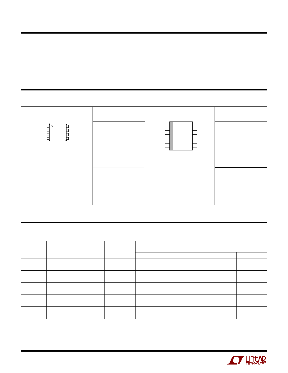
PACKAGE/ORDER I
N
FOR
M
ATIO
N
W
U
U
(Note 1)
Supply Voltage ........................................................ 13V
Input Voltages ........................................... 0.3V to 13V
Output Voltages ......................................... 0.3V to 13V
Output Short Circuit Duration .......................... Indefinite
LTC1258CMS8
LTC1258CMS8-2.5
LTC1258CMS8-3
LTC1258CMS8-4.1
LTC1258CMS8-5
T
JMAX
= 125
°
C,
JA
= 190
°
C/W
MS8 PART MARKING
LTEL
LTCF
LTEU
LTEN
LTEM
Consult factory for Industrial and Military grade parts.
1
2
3
4
8
7
6
5
TOP VIEW
DNC*
DNC*
DNC*
DNC*
OUT
IN
**DNC/FB
GND
S8 PACKAGE
8-LEAD PLASTIC SO
ORDER PART
NUMBER
Operating Temperature Range (Note 2) 40
°
C to 100
°
C
Specified Temperature Range ...................... 0
°
C to 70
°
C
Storage Temperature Range (Note 3) ....65
°
C to 150
°
C
Lead Temperature (Soldering, 10 sec).................. 300
°
C
1
2
3
4
OUT
IN
**DNC/FB
GND
8
7
6
5
DNC*
DNC*
DNC*
DNC*
TOP VIEW
MS8 PACKAGE
8-LEAD PLASTIC MSOP
T
JMAX
= 125
°
C,
JA
= 250
°
C/W
* CONNECTED INTERNALLY. DO NOT CONNECT
EXTERNAL CIRCUITRY TO THESE PINS
** DNC FOR LTC1258-2.5/LTC1258-3/LTC1258-4.1/
LTC1258-5, FB FOR LTC1258
LTC1258CS8
LTC1258CS8-2.5
LTC1258CS8-3
LTC1258CS8-4.1
LTC1258CS8-5
S8 PART MARKING
ORDER PART
NUMBER
1258
12582
12583
125841
12585
* CONNECTED INTERNALLY. DO NOT CONNECT
EXTERNAL CIRCUITRY TO THESE PINS
** DNC FOR LTC1258-2.5/LTC1258-3/LTC1258-4.1/
LTC1258-5, FB FOR LTC1258
OUTPUT
TEMPERATURE
TEMPERATURE
PACKAGE TYPE
VOLTAGE
RANGE
ACCURACY
COEFFICIENT S8
MS8
(V)
(
°
C)
(%)
(ppm/
°
C)
ORDER NUMBER
PART MARKING
ORDER NUMBER
PART MARKING
2.5
0 to 70
0.15
40
LTC1258CS8-2.5
12582
2.5
0 to 70
0.21
60
LTC1258CMS8-2.5
LTCF
3
0 to 70
0.15
40
LTC1258CS8-3
12583
3
0 to 70
0.20
60
LTC1258CMS8-3
LTEU
4.096
0 to 70
0.15
40
LTC1258CS8-4.1
125841
4.096
0 to 70
0.18
60
LTC1258CMS8-4.1
LTEN
5
0 to 70
0.15
40
LTC1258CS8-5
12585
5
0 to 70
0.18
60
LTC1258CMS8-5
LTEM
Adjustable
0 to 70
0.4
40
LTC1258CS8
1258
Adjustable
0 to 70
0.46
60
LTC1258CMS8
LTEL
AVAILABLE OPTIO S
U
3
LTC1258 Series
ELECTRICAL CHARACTERISTICS
V
IN
= V
OUT(NOMINAL)
+ 0.2V, I
OUT
= 0mA, FB = OUT for the LTC1258 unless otherwise noted.
SYMBOL
PARAMETER
CONDITIONS
MIN
TYP
MAX
UNITS
V
IN
Input Voltage Range
q
12.6
V
I
IN
Input Current
FB = OUT for LTC1258
6.5
µ
A
q
8.5
µ
A
V
OUT
Output Voltage (Note 4)
LTC1258 (S8), FB = OUT
2.3755
2.385
2.3945
V
LTC1258-2.5 (S8)
2.4963
2.5
2.5037
V
LTC1258-3 (S8)
2.9955
3
3.0045
V
LTC1258-4.1 (S8)
4.090
4.096
4.102
V
LTC1258-5 (S8)
4.9925
5
5.0075
V
LTC1258 (MS8), FB = OUT
2.374
2.385
2.396
V
LTC1258-2.5 (MS8)
2.4948
2.5
2.5052
V
LTC1258-3 (MS8)
2.994
3
3.006
V
LTC1258-4.1 (MS8)
4.0885
4.096
4.1035
V
LTC1258-5 (MS8)
4.991
5
5.009
V
e
n
Output Voltage Noise (Note 5)
0.1Hz
f
10Hz
8
ppm
P-P
TC
Output Voltage Temp Coefficient (Note 6)
T
MIN
T
J
T
MAX
(S8)
q
15
40
ppm/
°
C
T
MIN
T
J
T
MAX
(MS8)
q
60
ppm/
°
C
V
OUT
/V
IN
Line Regulation
V
IN
= (V
OUT(NOMINAL)
+ 0.2V) to 12.6V
q
30
90
ppm/V
V
OUT
/I
OUT
Load Regulation (Note 7)
Sourcing 0mA to 10mA
q
0.1
0.3
mV/mA
Sinking 0mA to 2mA
1.75
4.0
mV/mA
q
6.5
mV/mA
I
SC
Short-Circuit Output Current
V
OUT
Shorted to GND
20
40
mA
V
OUT
Shorted to V
IN
2
4
mA
V
DO
Dropout Voltage (Note 8)
I
OUT
= 0,
V
OUT
0.1%
q
100
mV
I
OUT
= 10mA,
V
OUT
0.1%
q
200
mV
V
HYST
Output Hysteresis (Note 9)
T = 40
°
C to 85
°
C
200
ppm
T = 0
°
C to 70
°
C
50
ppm
I
FB
FB Pin Input Current
LTC1258, OUT = FB
10
nA
The
q
denotes specifications which apply over the specified temperature range, otherwise specifications are TA = 25
°
C.
Note 1: Absolute Maximum Ratings are those values beyond which the life
of the device may be impaired.
Note 2: The LTC1258 is guaranteed functional over the operating
temperature range of 40
°
C to 100
°
C.
Note 3: If the part is stored outside of the specified operating temperature
range, the output may shift due to hysteresis.
Note 4: ESD (Electrostatic Discharge) sensitive device. Extensive use of
ESD protection devices are used internal to the LTC1258, however, high
electrostatic discharge can damage or degrade the device. Use proper ESD
handling precautions.
Note 5: Peak-to-peak noise is measured with a single pole highpass filter
at 0.1Hz and 2-pole lowpass filter at 10Hz.
Note 6: Temperature coefficient is the change in output voltage divided by
the nominal output voltage divided by the specified temperature range.
Note 7: Load regulation is measured on a pulse basis from no load to the
specified load current. Output changes due to die temperature change
must be taken into account separately.
Note 8: Dropout voltage is (V
IN
V
OUT
) when V
OUT
falls to 0.1% below its
nominal value at V
IN
= V
OUT
+ 0.5V.
Note 9: Hysteresis in output voltage is created by package stress that
differs depending on whether the IC was previously at a higher or lower
temperature. Output voltage is always measured at 25
°
C, but the IC is
cycled hot or cold before successive measurements. Hysteresis is not
normally a problem for operational temperature excursions where the
instrument might be stored at high or low temperature.
4
LTC1258 Series
TYPICAL PERFOR
M
A
N
CE CHARACTERISTICS
U
W
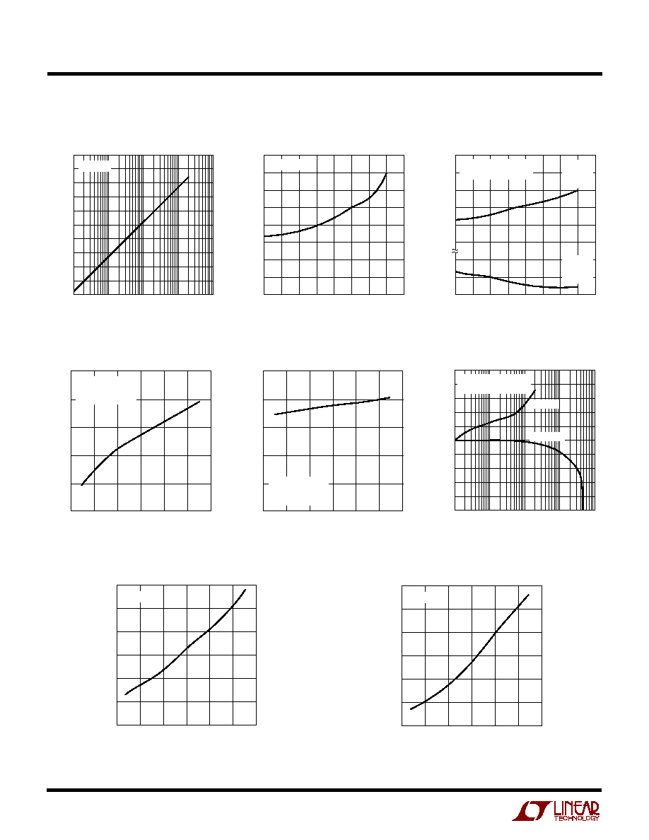
LTC1258-2.5* Output Short-Circuit
Current vs Input Voltage
LTC1258 Series
Load Regulation
INPUT VOLTAGE (V)
2
OUTPUT SHORT-CIRCUIT CURRENT (mA)
25
20
15
10
5
0
4
6
8
10
1258-G04
12
14
T
A
= 25
°
C
OUTPUT SHORTED
TO V
IN
INPUT VOLTAGE (V)
2
OUTPUT SHORT-CIRCUIT CURRENT (mA)
42
41
4
6
8
10
1258-G05
12
14
T
A
= 25
°
C
OUTPUT SHORTED
TO GND
OUTPUT CURRENT (mA)
V
OUT
FROM NO LOAD (mV)
5
4
3
2
1
0
1
2
3
4
5
0
1
10
100
1258 G06
0.1
T
A
= 25
°
C
V
IN
= V
OUT(NOM)
+ 0.2V
SINKING
SOURCING
LTC1258-2.5* Output Short-Circuit
Current vs Input Voltage
LTC1258-2.5
Output Voltage vs Input Voltage
LTC1258-2.5
Input Current vs Input Voltage
INPUT VOLTAGE (V)
2
OUTPUT VOLTAGE (V)
2.5010
2.5005
2.5000
2.4995
4
6
8
10
1258 G07
12
14
T
A
= 25
°
C
INPUT VOLTAGE (V)
2
INPUT CURRENT (
µ
A)
7
6
5
4
4
6
8
10
1258 G08
12
14
T
A
= 25
°
C
OUTPUT SOURCE CURRENT (mA)
DROPOUT VOLTAGE (mV)
100
90
80
70
60
50
40
30
20
10
0
0
1
10
100
1258 G01
0.1
T
A
= 25
°
C
TEMPERATURE (
°
C)
50 25
INPUT CURRENT (
µ
A)
150
1258 G02
0
25
50
75
100 125
8
7
6
5
4
3
2
1
0
V
IN
= 2.7V
TEMPERATURE (
°
C)
50 25
OUTPUT SHORT-CIRCUIT CURRENT (mA)
150
1258 G03
0
25
50
75
100 125
70
60
50
40
30
20
10
5
0
T
A
= 25
°
C
V
IN
= V
OUT(NOM)
+ 0.2V
OUTPUT
SHORTED
TO V
IN
OUTPUT
SHORTED
TO GND
LTC1258-2.5*
Dropout Voltage vs
Output Source Current
LTC1258-2.5*
Input Current vs Temperature
LTC1258 Series
Output Short-Circuit Current vs
Temperature
*Similar performance characteristics can be expected for all voltage options.
5
LTC1258 Series
PI
N
FU
N
CTIO
N
S
U
U
U
OUT (Pin 1): Reference Output. The output can source up
to 10mA and sink up to 2mA. It is stable with output bypass
capacitor ranging from 0
µ
F to 1
µ
F.
IN (Pin 2): Positive Supply. Bypassing with a 0.1
µ
F
capacitor is recommended if the output loading changes.
(V
OUT
+ 0.2V)
V
IN
12.6V.
DNC (Pin 3): (LTC1258-2.5/LTC1258-3/LTC1258-4.1/
LTC1258-5) Do Not Connect. Connected internally for
post package trim. This pin must be left unconnected.
FB (Pin 3): (LT1258) Resistor Divider Feedback Pin.
Connect a resistor divider from OUT to GND and the center
tap to FB. This pin sets the output potential.
V
V
R
R
R
OUT
=
+
2 385
1
2
2
.
; R1 is connected from OUT
to FB and R2 from FB to GND.
GND (Pin 4): Negative Supply or Ground Connection.
DNC (Pins 5, 6, 7, 8): Do Not Connect. Connected
internally for post package trim. These pins must be left
unconnected.
BLOCK DIAGRA
M
W
+
IN
1
1258 BD
2
4
OUT
3 (LTC1258)
FB
2.385V
GND
R1
R2
NOTE: R1 AND R2 ARE NOT CONNECTED FOR LTC1258
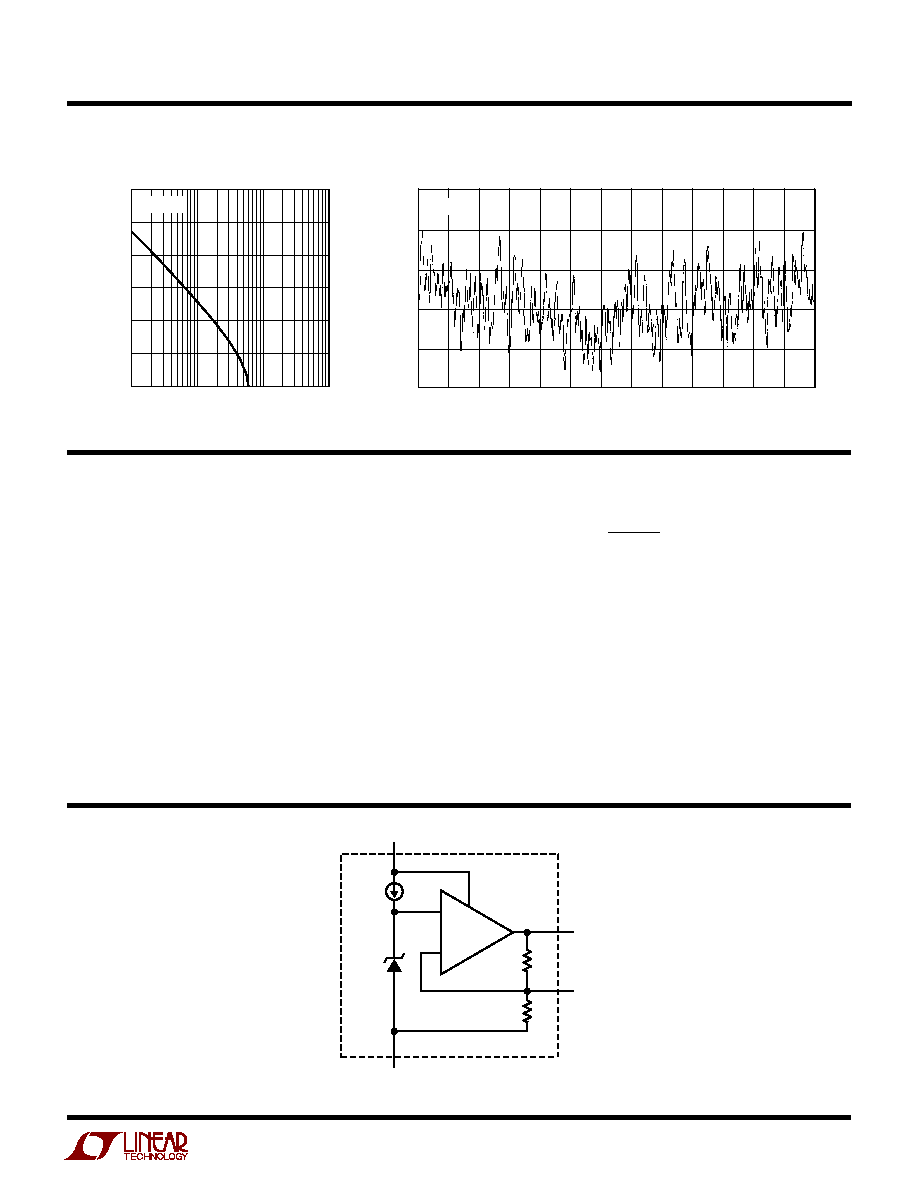
LTC1258-2.5 PSRR vs Frequency
5
µ
V/DIV
1258 G10
1SEC/DIV
V
IN
= 2.7V
LTC1258-2.5 0.1Hz to 10Hz Noise
FREQUENCY (Hz)
POWER SUPPLY REJECTION RATIO (dB)
60
50
40
30
20
10
0
10
1k
10k
1258 G09
100
V
IN
= 2.7V
TYPICAL PERFOR
M
A
N
CE CHARACTERISTICS
U
W