 | ÐлекÑÑоннÑй компоненÑ: LTC1348CG | СкаÑаÑÑ:  PDF PDF  ZIP ZIP |
Äîêóìåíòàöèÿ è îïèñàíèÿ www.docs.chipfind.ru
1
LTC1348
3.3V/5V Low Power RS232
3-Driver/5-Receiver Transceiver
S
FEATURE
D
U
ESCRIPTIO
s
Low Supply Current: 600
µ
A at 3.3V
s
Supply Current in Shutdown: 0.2
µ
A
s
Supply Current in Receiver Alive Mode: 15
µ
A
s
ESD Protection over
±
10kV
s
Operates from a Single 3V to 5.5V Supply
s
Operates to 120kBaud with 0.1
µ
F Flying Capacitors
s
Three-State Outputs Are High Impedance When Off
s
Output Overvoltage Does Not Force Current
Back into Supplies
s
RS232 I/O Lines Can Be Forced to
±
25V
Without Damage
s
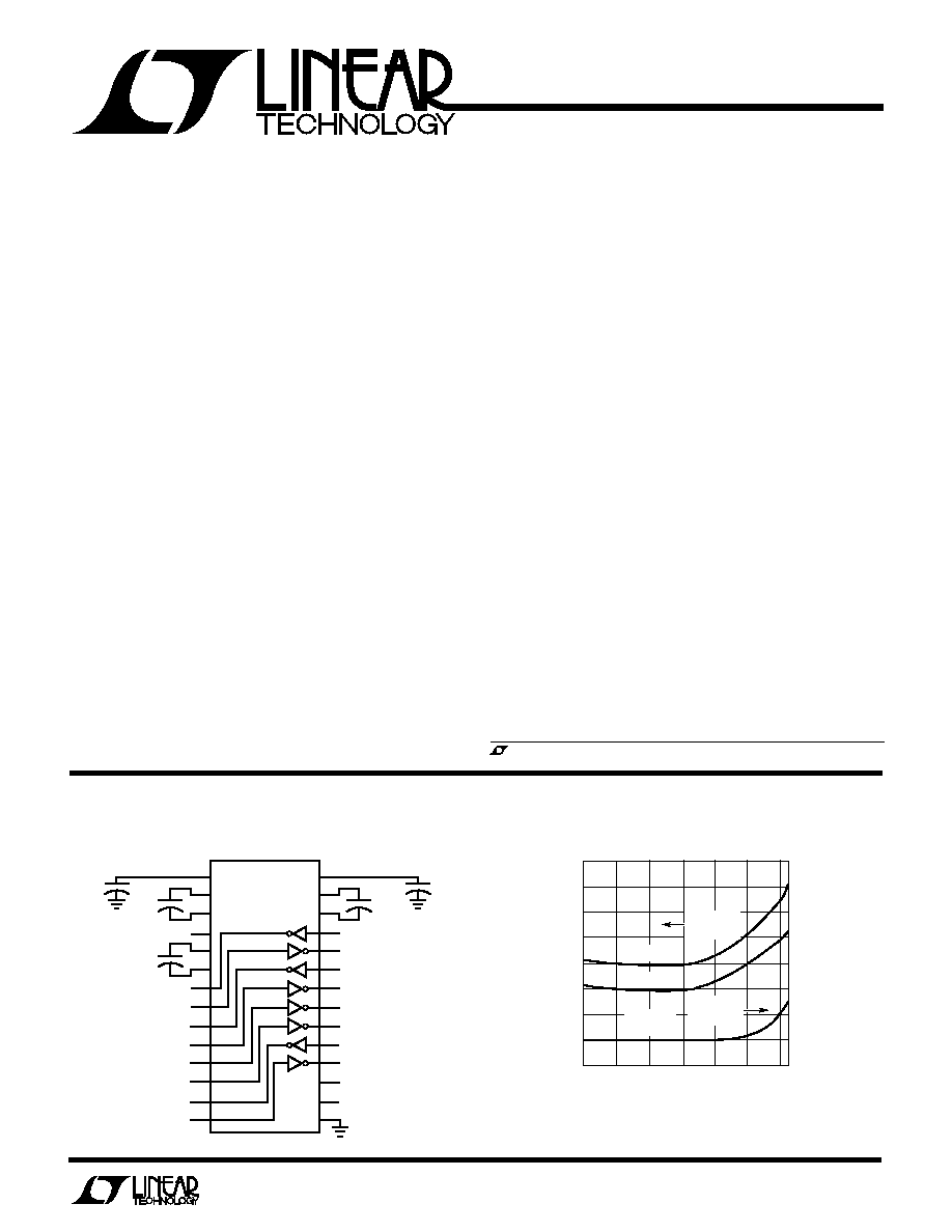
Flowthrough Architecture
The LTC
®
1348 is a 3-driver/5-receiver RS232 transceiver
with very low supply current. The charge pump only
requires five 0.1
µ
F capacitors. The LTC1348 provides full
RS232 output levels when operated over a wide supply
range of 3V to 5.5V
The transceiver operates in one of four modes: Normal,
Receiver Disable, Receiver Alive and Shutdown. In Normal
or Receiver Disable mode, I
CC
is only 600
µ
A at 3.3V and
800
µ
A at 5V in the no load condition. In Shutdown mode,
the supply current is further reduced to 0.2
µ
A. In Receiver
Alive mode, all five receivers are kept alive and the supply
current is 15
µ
A. All RS232 outputs assume a high imped-
ance state in Shutdown or Receiver Alive mode or with the
power off. The receiver outputs assume a high impedance
state in Receiver Disable or with the power off.
The LTC1348 is fully compliant with all data rate and
overvoltage RS232 specifications. The transceiver oper-
ates up to 120kbaud with all drivers loaded with 1000pF,
3k
. Both driver outputs and receiver inputs can be forced
to
±
25V without damage and can survive multiple
±
10kV
ESD strikes.
U
S
A
O
PPLICATI
s
Notebook Computers
s
Palmtop Computers
s
Printers
s
Portable Instruments
LT1348 · TA01
C5
0.1
µ
F
C2
0.1
µ
F
C3
0.1
µ
F
C4
0.1
µ
F
LTC1348
1
2
3
4
5
6
7
8
9
10
11
12
13
14
DR 1 OUT
RX1 IN
DR 2 OUT
RX2 IN
RX3 IN
RX4 IN
DR 3 OUT
RX5 IN
28
27
26
25
24
23
22
21
20
19
18
17
16
15
DR 1 IN
RX1 OUT
DR 2 IN
RX2 OUT
RX3 OUT
RX4 OUT
DR 3 IN
RX5 OUT
DREN
RXEN
V
V
+
V
CC
GND
C1
0.1
µ
F
3-Drivers/5-Receivers with Shutdown
U
A
O
PPLICATI
TYPICAL
Supply Current
, LTC and LT are registered trademarks of Linear Technology Corporation.
TEMPERATURE (°C)
40
SUPPLY CURRENT (mA)
1.4
20
LT1348 ·TA02
0.8
0.4
20
0
40
0.2
0
1.6
1.2
1.0
0.6
SHUTDOWN CURRENT (
µ
A)
1.4
0.8
0.4
0.2
0
1.6
1.2
1.0
0.6
60
80
QUIESCENT
CURRENT
SHUTDOWN
CURRENT
V
CC
= 5V
V
CC
= 3.3V
V
CC
= 3.3V
OR 5V
2
LTC1348
A
U
G
W
A
W
U
W
A
R
BSOLUTE
XI
TI
S
W
U
U
PACKAGE/ORDER I FOR ATIO
ORDER PART
NUMBER
LTC1348CG
LTC1348CSW
LTC1348IG
LTC1348ISW
(Note 1)
Supply Voltage (V
CC
) ................................................ 6V
Input Voltage
Driver ....................................... 0.3V to V
CC
+ 0.3V
Receiver ............................................... 25V to 25V
Driver/Receiver Enable Pin ........ 0.3V to V
CC
+ 0.3V
Output Voltage
Driver ................................................... 25V to 25V
Receiver .................................... 0.3V to V
CC
+ 0.3V
Short-Circuit Duration
V
+
................................................................... 30 sec
V
................................................................... 30 sec
Driver Output .............................................. Indefinite
Receiver Output .......................................... Indefinite
Operating Temperature Range
LTC1348C................................................ 0
°
C to 70
°
C
LTC1348I ............................................ 40
°
C to 85
°
C
Storage Temperature Range ................ 65
°
C to 150
°
C
Lead Temperature (Soldering, 10 sec)................. 300
°
C
Consult factory for Military grade parts.
1
2
3
4
5
6
7
8
9
10
11
12
13
14
V
+
C2
+
C2
V
CC
C1
+
C1
DR1 OUT
RX1 IN
DR2 OUT
RX2 IN
RX3 IN
RX4 IN
DR3 OUT
RX5 IN
28
27
26
25
24
23
22
21
20
19
18
17
16
15
V
C3
+
C3
DR1 IN
RX1 OUT
DR2 IN
RX2 OUT
RX3 OUT
RX4 OUT
DR3 IN
RX5 OUT
DREN
RXEN
GND
TOP VIEW
SW PACKAGE
28-LEAD PLASTIC SO
G PACKAGE
28-LEAD PLASTIC SSOP
T
JMAX
= 125
°
C,
JA
= 96
°
C/W (G)
T
JMAX
= 125
°
C,
JA
= 85
°
C/W (SW)
ELECTRICAL C
C
HARA TERISTICS
C
D
V
CC
= 3V to 5.5V, C1 to C4 = 0.1
µ
F, unless otherwise noted.
PARAMETER
CONDITIONS
MIN
TYP
MAX
UNITS
Any Driver
Output Voltage Swing
V
CC
= 3.3V, 3k to GND
Positive
q
5.0
6.2
V
Negative
q
5.0
6.0
V
Logic Input Voltage Level
Input Low Level (V
OUT
= High)
q
0.8
V
Input High Level (V
OUT
= Low), V
CC
= 3.3V
q
2.0
V
Input High Level (V
OUT
= Low), V
CC
= 5V
q
2.4
V
Logic Input Current
V
IN
= V
CC
q
5
µ
A
V
IN
= 0V
q
5
35
µ
A
Output Short-Circuit Current
V
OUT
= 0V
±
12
mA
Output Leakage Current
Shutdown (Note 3) or Receiver Alive Mode (Note 4),
q
±
10
±
500
µ
A
V
OUT
=
±
20V
Any Receiver
Input Voltage Thresholds
Input Threshold (Receiver Alive Mode)
0.8
1.5
2.4
V
Input Low Threshold (Normal Mode)
0.8
1.3
V
Input High Threshold (Normal Mode)
1.7
2.4
V
Hysteresis
Normal Mode
0.3
V
Input Resistance
V
IN
=
±
10V
3
5
7
k
Output Voltage
Output Low, I
OUT
= 1.6mA
q
0.2
0.4
V
Output High, I
OUT
= 160
µ
A
q
V
CC
0.6V
V
Output Short-Circuit Current
Sinking Current, V
OUT
= V
CC
3
20
mA
Output Leakage Current
Shutdown (Note 3), 0V
V
OUT
V
CC
q
1
10
µ
A
3
LTC1348
ELECTRICAL C
C
HARA TERISTICS
C
D
V
CC
= 3V to 5.5V, C1 to C4 = 0.1
µ
F, unless otherwise noted.
PARAMETER
CONDITIONS
MIN
TYP
MAX
UNITS
Power Supply Generator
V
+
Output Voltage
I
OUT
= 0mA
8.0
V
I
OUT
= 8mA
7.5
V
V
Output Voltage
I
OUT
= 0mA
8.0
V
I
OUT
= 8mA
7.0
V
Supply Rise Time
Shutdown to Turn-On
0.2
ms
Power Supply
V
CC
Supply Current
No Load (Note 2) V
CC
= 3.3V
q
0.6
2.0
mA
No Load (Note 2) V
CC
= 5V
q
0.8
2.5
mA
Receiver Alive Mode (Note 4) V
CC
= 3.3V or 5V
q
15
30
µ
A
Supply Leakage Current (V
CC
)
Shutdown (Note 3)
q
0.2
10
µ
A
Driver/Receiver Enable Threshold Low
q
0.8
V
Driver/Receiver Enable Threshold High
V
CC
= 3.3V
q
2.0
V
Driver/Receiver Enable Threshold High
V
CC
= 5V
q
2.4
V
AC ELECTRICAL CHARACTERISTICS
PARAMETER
CONDITIONS
MIN
TYP
MAX
UNITS
Maximum Data Rate
R
L
= 3k, C
L
= 1000pF, One Driver Switching
120
250
kbps
Slew Rate
V
CC
= 5V, R
L
= 3k, C
L
= 51pF
8
30
V/
µ
s
V
CC
= 3.3V, R
L
= 3k, C
L
= 2500pF
3
V/
µ
s
Driver Propagation Delay
t
HLD
(Figure 1)
q
2.5
4
µ
s
(TTL to RS232)
t
LHD
(Figure 1)
q
2.5
4
µ
s
Receiver Propagation Delay
t
HLR
(Figure 2) (Normal Mode)
q
0.3
1
µ
s
(RS232 to TTL)
t
LHR
(Figure 2) (Normal Mode)
q
0.2
1
µ
s
t
HLR
(Figure 2) (Receiver Alive Mode)
q
1.0
4
µ
s
t
LHR
(Figure 2) (Receiver Alive Mode)
q
0.2
4
µ
s
Note 3: Supply current measurement in Shutdown is performed with
V
DREN
and V
RXEN
= 0V.
Note 4: Supply current measurement in Receiver Alive mode is performed
with V
DREN
= 0V and V
RXEN
= V
CC
.
V
CC
= 3V to 5.5V, C1 to C4 = 0.1
µ
F, unless otherwise noted.
The
q
denotes specifications which apply over the full operating
temperature range (0
°
C
T
A
70
°
C for Commercial grade and
40
°
C
T
A
85
°
C for Industrial grade).
Note 1: Absolute Maximum Ratings are those values beyond which the life
of the device may be impaired.
Note 2: Supply current is measured with driver and receiver outputs
unloaded. The V
DREN
and V
RXEN
= V
CC
.
4
LTC1348
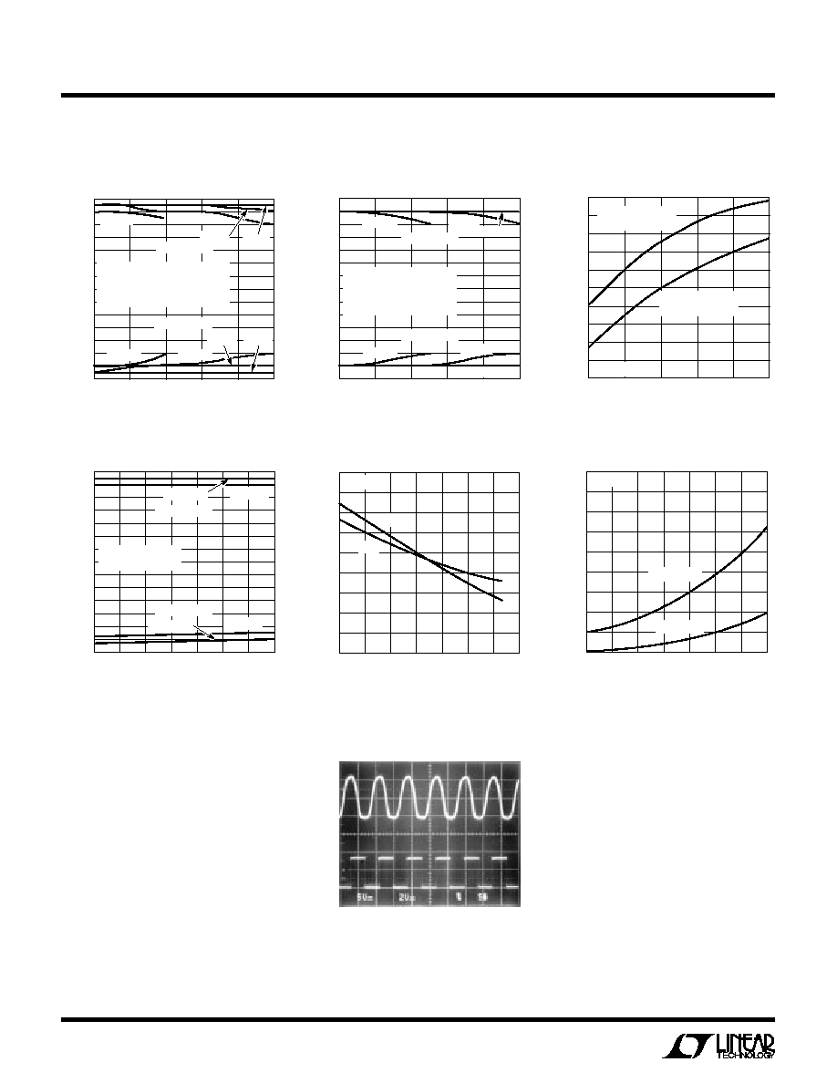
TYPICAL PERFOR
M
A
N
CE CHARACTERISTICS
U
W
Driver Output Voltage High/Low
vs Load Capacitance (C
L
)
Supply Current
vs Driver Data Rate
Driver Output Voltage High/Low
vs Load Capacitance (C
L
)
Driver Output Voltage High/Low
vs Temperature (
°
C)
TEMPERATURE (
°
C)
0
0
LEAKAGE CURRENT (
µ
A)
5
15
20
25
50
45
LTC1348 G06
10
20
10
30
40
60
70
30
35
40
V
OUT
= 20V
V
OUT
= 20V
V
CC
= 3.3V
LOAD CAPACITANCE (pF)
0
7
DRIVER OUTPUT VOLTAGE HIGH/LOW
5
3
1
7
6
4
2
0
2
4
6
3
1000
2000
5000
5
1
3000
4000
250kbps
250kbps
120kbps
120kbps
64kbps
64kbps 20kbps
20kbps
V
CC
= 3.3V
0.1
µ
F FLYING CAPACITORS
ALL DRIVERS LOADED 3k
+ C
L
1 DRIVER DRIVEN
LTC1348 G01
OUTPUT HIGH
OUTPUT LOW
LOAD CAPACITANCE (pF)
0
7
DRIVER OUTPUT VOLTAGE HIGH/LOW
5
3
1
7
6
4
2
0
2
4
6
3
1000
2000
5000
5
1
3000
4000
120kbps
120kbps
64kbps
64kbps
20kbps
V
CC
= 3.3V
0.1
µ
F FLYING CAPACITORS
ALL DRIVERS DRIVEN AND
LOADED 3k
+ C
L
LTC1348 G02
OUTPUT HIGH
OUTPUT LOW
20kbps
Driver Leakage in SHUTDOWN
vs Temperature (
°
C)
TEMPERATURE (
°
C)
0
7
DRIVER OUTPUT VOLTAGE HIGH/LOW
5
3
1
7
6
4
2
0
2
4
6
3
10
20
30
70
5
1
40
50
60
LTC1348 G04
V
CC
= 3V
V
CC
= 3V
V
CC
= 3.3V
OUTPUT HIGH
OUTPUT LOW
V
CC
= 3.3V
ALL DRIVERS
LOADED WITH 3k
Driver Short-Circuit Current
vs Temperature (
°
C)
With V
CC
= 3.3V
All Driver Outputs Loaded with
3k
, 1000pF. 1 Driven at 250kbps
DRIVER DATA RATE
0
SUPPLY CURRENT (mA)
30
40
50
200
LTC1348 G03
20
10
0
50
100
150
250
3 OUTPUT LOADED
3k
// 2500pF
1 OUTPUT LOADED
3k
// 2500pF
V
CC
= 3.3V
TEMPERATURE (
°
C)
40
0
SHORT-CIRCUIT CURRENT (mA)
4
8
10
12
60
20
LTC1348 G05
6
0
20
20
40
80
100
14
16
18
I
SC
I
SC
+
V
CC
= 3.3V
LTC1348 G07
DRIVER
INPUT
DRIVEN DRIVER
OUTPUT

5
LTC1348
PI FU CTIO S
U
U
U
V
CC
: 3V to 5.5V Input Supply Pin. This pin should be
decoupled with a 0.1
µ
F ceramic capacitor.
GND: Ground Pin.
RXEN: TTL/CMOS Compatible Enable Pin. Refer to Table
1 for its functional description.
DREN: TTL/CMOS Compatible Enable Pin. Refer to Table
1 for its functional description.
V
+
: Positive Supply Output (RS232 Drivers). This pin
requires an external capacitor C = 0.1
µ
F for charge stor-
age. The capacitor may be tied to ground or V
CC
. With
multiple devices, the V
+
and V
pins may be paralleled into
common capacitors. For large numbers of devices, in-
creasing the size of the shared common storage capaci-
tors is recommended to reduce ripple.
V
: Negative Supply Output (RS232 Drivers). This pin
requires an external capacitor C = 0.1
µ
F for charge
storage.
C1
+
, C1
, C2
+
, C2
, C3
+
, C3
: Commutating Capacitor
Inputs. These pins require three external capacitors C =
0.1
µ
F: one from C1
+
to C1
, another from C2
+
to C2
and
another from C3
+
to C3
. To maintain charge pump
efficiency, the capacitor's effective series resistance should
be less than 1
. Ceramic capacitors are recommended.
DR IN: RS232 Driver Input Pins. Inputs are TTL/CMOS
compatible. The inputs of unused drivers can be left
unconnected since 300k input pull-up resistors to V
CC
are
included on chip. To minimize power consumption, the
internal driver pull-up resistors are disconnected from V
CC
in the Shutdown or Receiver Alive mode.
DR OUT: Driver Outputs at RS232 Voltage Levels. Outputs
are in a high impedance state when in the Shutdown,
Receiver Alive mode or V
CC
= 0V. The driver outputs are
protected against ESD to
±
10kV for human body model
discharges.
RX IN: Receiver Inputs. These pins can be forced to
±
25V
without damage. The receiver inputs are protected against
ESD to
±
10kV for human body model discharges. Each
receiver provides 0.4V of hysteresis for noise immunity. In
Receiver Alive mode all receivers have no hysteresis.
RX OUT: Receiver Outputs with TTL/CMOS Voltage Lev-
els. Outputs are in a high impedance state when in the
Shutdown or Receiver Disable mode to allow data line
sharing.
Table 1. Functional Description
MODE
RX ENABLE
DR ENABLE
DRIVERS
RECEIVERS
I
CC
TYP
Shutdown
0
0
All Drivers Shutdown.
All Receivers Shutdown.
0.2
µ
A
All Driver Outputs Assume High Impedance.
All Receiver Outputs Assume High Impedance.
All Driver Pull-Up Resistors Disconnect
From V
CC
.
Receiver
0
1
All Drivers Alive.
All Receiver Outputs in Three-State.
600
µ
A at
Disable
3.3V,
800
µ
A at
5V
Receiver
1
0
All Drivers Shutdown.
All Receivers Alive.
15
µ
A
Alive
All Driver Outputs in Three-State.
All Driver Pull-Up Resistors Disconnect
From V
CC
.
Normal
1
1
All Drivers Alive.
All Receivers Alive.
600
µ
A at
3.3V,
800
µ
A at
5V