 | ÐлекÑÑоннÑй компоненÑ: LTC1384IG | СкаÑаÑÑ:  PDF PDF  ZIP ZIP |
1384fa.pm7
1
LTC1384
1384fa
The LTC
®
1384 is an ultra-low power 2-driver/2-receiver
RS232 transceiver that operates from a single 5V
supply. The charge pump requires only four space-
saving 0.1µF capacitors.
The transceiver operates in one of two modes, Normal and
Shutdown. In the Normal mode, I
CC
is only 220µA with the
driver outputs unloaded. In the Shutdown mode, the
charge pump is turned off, the driver outputs are forced
into three-state, both receivers are kept active and I
CC
drops to 35µA. The receiver outputs may be forced into
three-state at any time using the receiver enable (RX EN)
pin.
The LTC1384 is fully compliant with all data rate and
overvoltage RS232 specifications. The transceiver can
operate up to 120kbaud with a 2500pF, 3k load. Both
driver outputs and receiver inputs can be forced to
±25V without damage and can survive multiple ±10kV
ESD strikes.
5V Low Power RS232
Transceiver with 2 Receivers
Active in Shutdown
Operates from a Single 5V Supply
Low Supply Current: I
CC
= 220µA
I
CC
= 35µA in Shutdown Mode with Both
Receivers Kept Alive
ESD Protection Over ±10kV
Uses Small Capacitors: 0.1µF
Operates to 120kBaud
Output Overvoltage Does Not Force Current
Back into Supplies
RS232 I/O Lines Can Be Forced to ±25V
Without Damage
Pin Compatible with LT1180A
Notebook Computers
Palmtop Computers
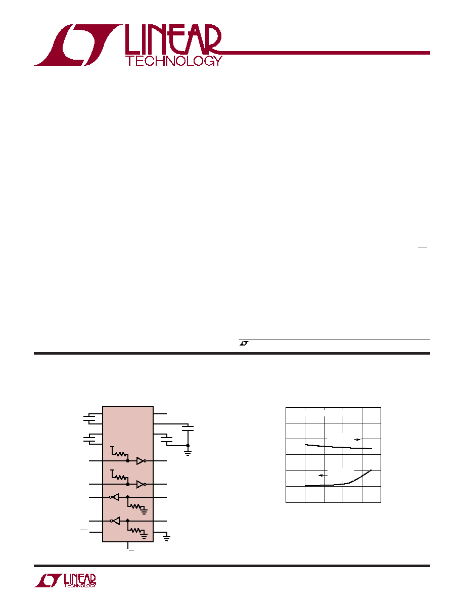
2-Drivers/2-Receivers with Shutdown
and Receiver Enable
Quiescent and Shutdown Supply Current
vs Temperature
TEMPERATURE (°C)
20
0
QUIESCENT CURRENT (
µ
A)
200
400
600
800
1200
0
20
40
60
LTC1384 · TA02
80
1000
TEST CONDITION: V
CC
= 5V
0
SHUTDOWN CURRENT (
µ
A)
10
20
30
40
60
50
QUIESCENT
CURRENT
SHUTDOWN
CURRENT
FEATURES
DESCRIPTIO
U
APPLICATIO S
U
TYPICAL APPLICATIO
U
, LTC and LT are registered trademarks of Linear Technology Corporation.
LTC1384 · TA01
LTC1384
2
4
0.1µF
17
V
CC
= 5V
3
0.1µF
7
0.1µF
0.1µF
5
6
232 OUTPUT
15
8
232 OUTPUT
14
232 INPUT
5k
9
232 INPUT
16
12
11
13
10
LOGIC INPUT
LOGIC INPUT
LOGIC OUTPUT
LOGIC OUTPUT
5k
18
ON/OFF
RX EN
1
300k
V
CC
300k
V
CC
2
LTC1384
1384fa
Supply Voltage (V
CC
) ................................................ 6V
Input Voltage
Driver ....................................... 0.3V to V
CC
+ 0.3V
Receiver ............................................... 25V to 25V
Digital Input ............................... 0.3V to V
CC
+ 0.3V
Output Voltage
Driver .................................................... 25V to 25V
Receiver .................................... 0.3V to V
CC
+ 0.3V
Short-Circuit Duration
V
+
................................................................... 30 sec
V
................................................................... 30 sec
Driver Output .............................................. Indefinite
Receiver Output .......................................... Indefinite
Operating Temperature Range
LTC1384C ............................................... 0°C to 70°C
LTC1384I ............................................ 40°C to 85°C
Storage Temperature Range ................. 65°C to 150°C
Lead Temperature (Soldering, 10 sec)................. 300°C
ORDER PART
NUMBER
ORDER PART
NUMBER
Consult LTC Marketing for parts specified with wider operating temperature ranges.
LTC1384CG
LTC1384IG
1
2
3
4
5
6
7
8
9
10
TOP VIEW
G PACKAGE
20-LEAD SSOP
20
19
18
17
16
15
14
13
12
11
C1
+
V
+
C1
C2
+
C2
V
TR2 OUT
RX2 IN
NC
ON/OFF
VCC
GND
TR1 OUT
RX1 IN
RX1 OUT
TR1 IN
TR2 IN
RX2 OUT
NC
RX EN
T
JMAX
= 125°C,
JA
= 135°C/W
T
JMAX
= 125°C,
JA
= 65°C/W
1
2
3
4
5
6
7
8
9
TOP VIEW
SW PACKAGE
18-LEAD PLASTIC SO
18
17
16
15
14
13
12
11
10
RX EN
C1
+
V
+
C1
C2
+
C2
V
TR2 OUT
RX2 IN
ON/OFF
V
CC
GND
TR1 OUT
RX1 IN
RX1 OUT
TR1 IN
TR2 IN
RX2 OUT
N PACKAGE
18-LEAD PDIP
LTC1384CN
LTC1384CSW
LTC1384IN
LTC1384ISW
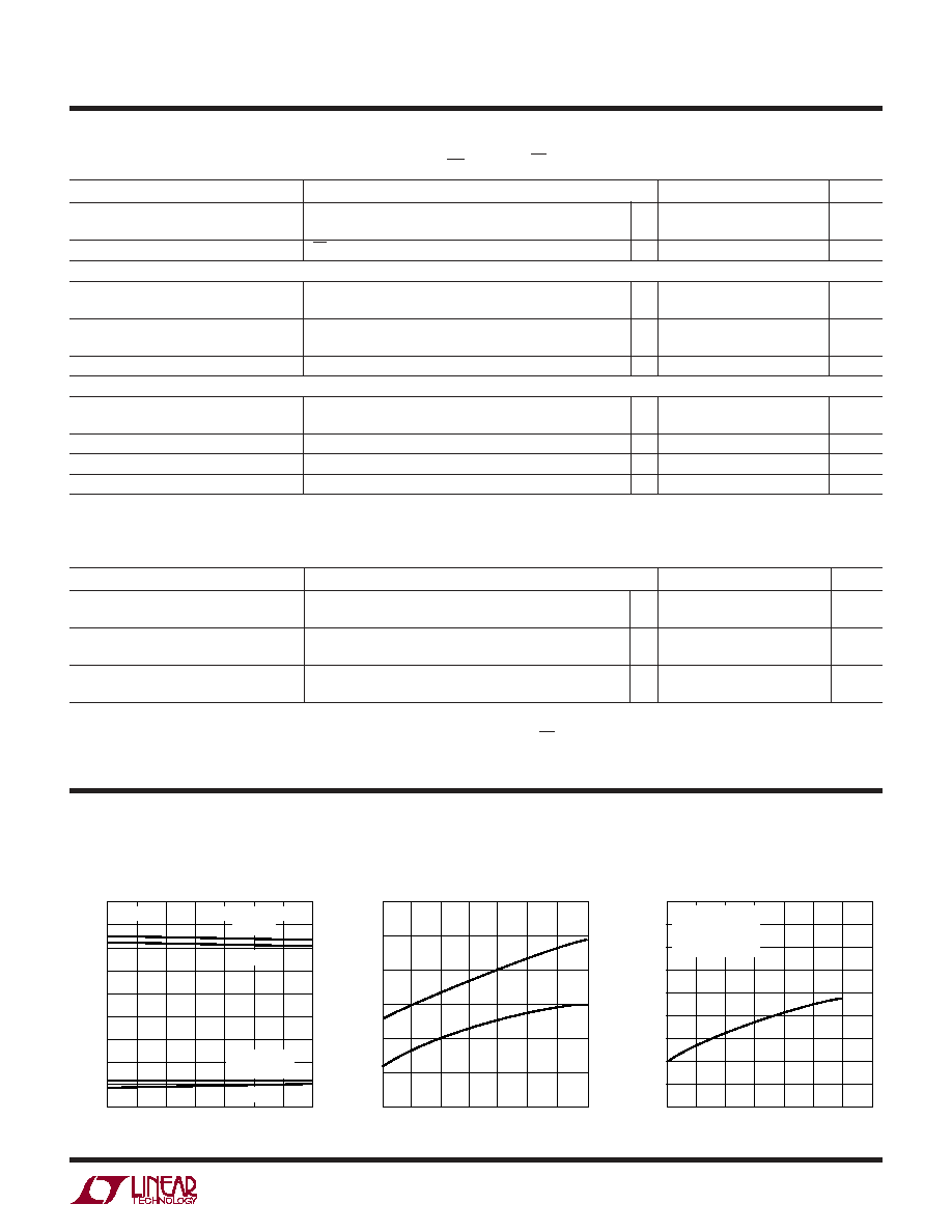
DC ELECTRICAL CHARACTERISTICS
PARAMETER
CONDITIONS
MIN
TYP
MAX
UNITS
Any Driver
Output Voltage Swing
3k to GND
Positive
5.0
7.0
V
Negative
5.0
6.5
V
Logic Input Voltage Level
Input Low Level (V
OUT
= High)
1.4
0.8
V
Input High Level (V
OUT
= Low)
2.0
1.4
V
Logic Input Current
V
IN
= V
CC
5
µA
V
IN
= 0V
20
40
µA
Output Short-Circuit Current
V
OUT
= 0V
±9
±12
mA
Output Leakage Current
Shutdown or V
CC
= 0V (Note 3), V
OUT
= ±10V
±10
±500
µA
Any Receiver
Input Voltage Thresholds
Input Low Threshold
0.8
1.3
V
Input High Threshold
1.7
2.4
V
Hysteresis
0.1
0.4
1
V
Input Resistance
10V V
IN
10V
3
5
7
k
Output Voltage
Output Low, I
OUT
= 1.6mA (V
CC
= 5V)
0.2
0.4
V
Output High, I
OUT
= 160µA (V
CC
= 5V)
3.0
3.2
V
T
JMAX
= 125°C,
JA
= 85°C/W
PACKAGE/ORDER I FOR ATIO
U
U
W
ABSOLUTE AXI U RATI GS
W
W
W
U
The
denotes specifications which apply over the full operating
temperature range. V
CC
= 5V, C1 = C2 = C3 = C4 = 0.1µF, V
ON/OFF
= V
CC
, RX EN = 0V, unless otherwise noted.
3
LTC1384
1384fa
DC ELECTRICAL CHARACTERISTICS
AC CHARACTERISTICS
Note 1: Absolute Maximum Ratings are those values beyond which the life
of the device may be impaired.
Note 2: Supply current is measured with driver and receiver outputs
unloaded.
Note 3: Measurements made in the Shutdown mode are performed
with V
ON/OFF
= 0V.
PARAMETER
CONDITIONS
MIN
TYP
MAX
UNITS
Slew Rate
R
L
= 3k, C
L
= 51pF
8
30
V/µs
R
L
= 3k, C
L
= 2500pF
3
5
V/µs
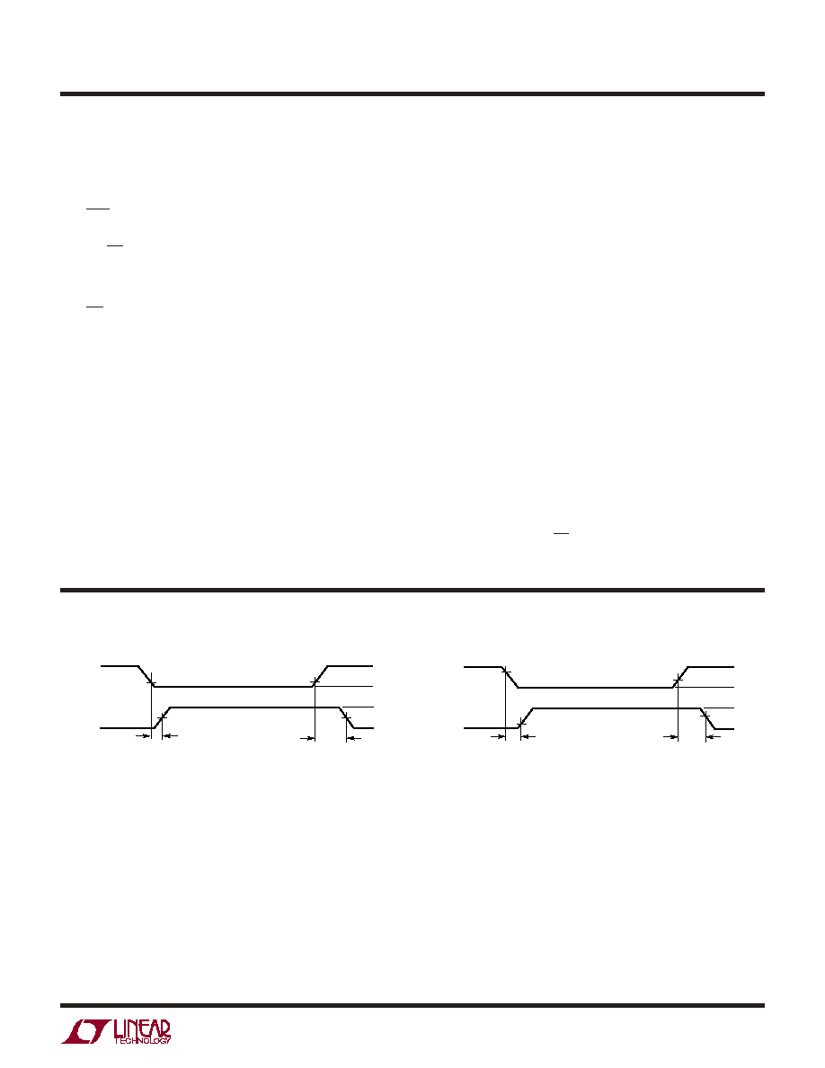
Driver Propagation Delay
t
HLD
(Figure 1)
2
3.5
µs
(TTL to RS232)
t
LHD
(Figure 1)
2
3.5
µs
Receiver Propagation Delay
t
HLR
(Figure 2)
0.3
0.8
µs
(RS232 to TTL)
t
LHR
(Figure 2)
0.3
0.8
µs
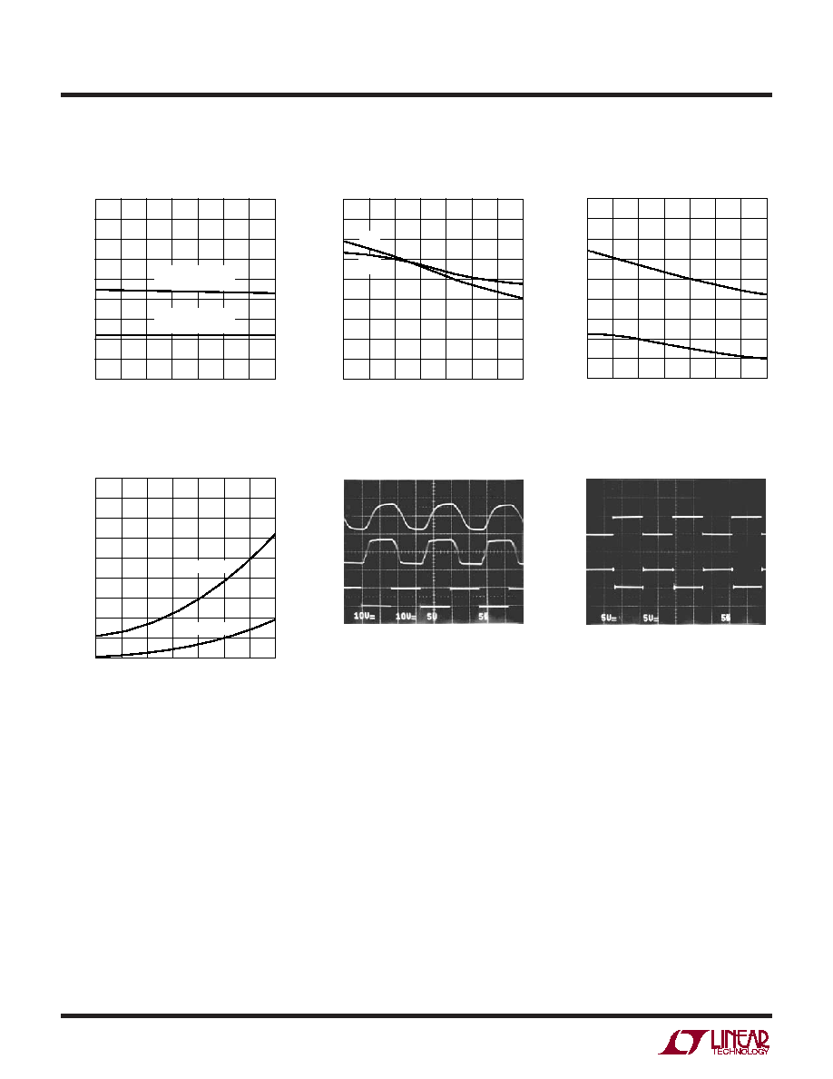
Driver Output Voltage
vs Temperature
TEMPERATURE (°C)
0
THRESHOLD VOLTAGE (V)
1.8
2.0
2.2
30
50
V
TH
V
TL
1.6
1.4
10
20
40
60
70
1.2
1.0
DATA RATE (kBAUD)
0
0
SUPPLY CURRENT (mA)
5
15
20
25
100
45
10
50
25
125
75
150
175
30
35
40
V
CC
= 5V
R
L
= 3k
C
L
= 2500pF
2 DRIVERS ACTIVE
Receiver Input Thresholds
vs Temperature
Supply Current vs Data Rate
TYPICAL PERFOR A CE CHARACTERISTICS
U
W
TEMPERATURE (°C)
0
8
DRIVER OUTPUT VOLTAGE (V)
6
2
0
2
40
10
4
20
10
50
60
30
70
4
6
8
R
L
= 3k
V
CC
= 5V
V
CC
= 4.5V
OUTPUT HIGH
V
CC
= 4.5V
V
CC
= 5V
OUTPUT LOW
The
denotes specifications which apply over the full operating temperature range.
V
CC
= 5V, C1 = C2 = C3 = C4 = 0.1µF,unless otherwise noted.
PARAMETER
CONDITIONS
MIN
TYP
MAX
UNITS
Output Short-Circuit Current
Sinking Current, V
OUT
= V
CC
15
40
mA
Sourcing Current, V
OUT
= 0V
10
20
mA
Output Leakage Current
EN = V
CC
, 0V V
OUT
V
CC
1
10
µA
Power Supply Generator
V
+
Output Voltage
I
OUT
= 0mA
8.0
V
I
OUT
= 8mA
7.5
V
V
Output Voltage
I
OUT
= 0mA
8.0
V
I
OUT
= 8mA
7.0
V
Supply Rise Time
Shutdown to Turn-On
0.2
ms
Power Supply
V
CC
Supply Current
No Load (Note 2), 0°C to 70°C
0.22
0.5
mA
No Load (Note 2), 40°C to 85°C
0.35
1.0
mA
Supply Leakage Current (V
CC
)
Shutdown (Note 3)
35
50
µA
Digital Input Threshold Low
1.4
0.8
V
Digital Input Threshold High
2.0
1.4
V
The
denotes specifications which apply over the full operating
temperature range. V
CC
= 5V, C1 = C2 = C3 = C4 = 0.1µF, V
ON/OFF
= V
CC
, RX EN = 0V, unless otherwise noted.
4
LTC1384
1384fa
V
CC
Supply Current
vs Temperature
Driver Short-Circuit Current
vs Temperature
TEMPERATURE (°C)
0
0
SUPPLY CURRENT (mA)
2
6
8
10
40
18
LTC1384 · TPC04
4
20
10
50
30
60
70
12
14
16
2 DRIVERS LOADED
R
L
= 3k
1 DRIVER LOADED
R
L
= 3k
TEMPERATURE (°C)
0
0
SHORT-CIRCUIT CURRENT (mA)
2
6
8
10
40
18
LTC1384 · TPC05
4
20
10
50
30
60
70
12
14
16
I
SC
I
SC
+
Receiver Short-Circuit Current
vs Temperature
TEMPERATURE (°C)
0
10
SHORT-CIRCUIT CURRENT (mA)
30
20
40
LTC1384 · TPC06
20
10
I
SC
+
I
SC
50
30
60
70
40
50
Driver Leakage in Shutdown
vs Temperature
TEMPERATURE (°C)
0
LEAKAGE CURRENT (
µ
A)
60
45
40
35
30
25
20
15
10
5
0
LTC1384 · TPC07
20
70
10
30
40
50
V
OUT
= 20V
V
OUT
= 20V
Driver Output Waveforms
Receiver Output Waveforms
LTC1384 · TPC08
INPUT
RECEIVER
OUTPUT
C
L
= 51pF
INPUT
LTC1384 · TPC09
DRIVER
OUTPUT
R
L
= 3k
C
L
= 2500pF
DRIVER
OUTPUT
R
L
= 3k
5µs/DIV
5µs/DIV
TYPICAL PERFOR A CE CHARACTERISTICS
U
W
5
LTC1384
1384fa
V
CC
: 5V Input Supply Pin. This pin should be decoupled
with a 0.1µF ceramic capacitor.
GND: Ground Pin.
ON/OFF: TTL/CMOS Compatible Shutdown Pin. A logic
low puts the device in the Shutdown mode independent of
the RX EN pin. The supply current of the device drops to
35µA (two receivers alive) and both driver outputs are
forced into three-state.
RX EN: TTL/CMOS Compatible Receiver Enable Pin. A
logic high forces the receiver outputs into three-state. A
logic low enables the receiver outputs.
V
+
: Positive Supply Output (RS232 Drivers). V
+
2V
CC
2V. This pin requires an external capacitor C = 0.1µF for
charge storage. The capacitor may be tied to ground or
V
CC
. With multiple devices, the V
+
and V
pins may share
a common capacitor. For large numbers of devices, in-
creasing the size of the shared common storage capaci-
tors is recommended to reduce ripple.
V
: Negative Supply Output (RS232 Drivers). V
(2V
CC
2V). This pin requires an external capacitor C = 0.1µF for
charge storage.
Figure 1. Driver Propagation Delay Timing
Figure 2. Receiver Propagation Delay Timing
1.4V
0V
V
CC
0V
V
+
V
0V
DRIVER
INPUT
DRIVER
OUTPUT
1.4V
t
HLD
t
LHD
LTC1384 · F01
0.8V
V
CC
0V
2.4V
RX
INPUT
RX
OUTPUT
1.3V
t
HLR
1.7V
t
LHR
LTC1384 · F02
V
CC
0V
SWITCHI G TI E WAVEFOR S
U
W
W
C1
+
, C1
, C2
+
, C2
: Commutating Capacitor Inputs. These
pins require two external capacitors C = 0.1µF: one from
C1
+
to C1
and another from C2
+
to C2
. To maintain
charge pump efficiency, the capacitor's effective series
resistance should be less than 2.
TR IN: RS232 Driver Input Pins. Inputs are TTL/CMOS
compatible. The inputs of unused drivers can be left
unconnected since 300k input pull-up resistors to V
CC
are
included on chip. To minimize power consumption, the
internal driver pull-up resistors are disconnected from V
CC
in the Shutdown mode.
TR OUT: Driver Outputs at RS232 Voltage Levels. Outputs
are in a high impedance state when in the Shutdown or V
CC
= 0V. The driver outputs are protected against ESD to
±10kV for human body model discharges.
RX IN: Receiver Inputs. These pins can be forced to ±25V
without damage. The receiver inputs are protected against
ESD to ±10kV for human body model discharges. Each
receiver provides 0.4V of hysteresis for noise immunity.
RX OUT: Receiver Outputs with TTL/CMOS Voltage Lev-
els. A logic high at RX EN puts the outputs into three-state.
U
U
U
PI FU CTIO S