 | –≠–ª–µ–∫—Ç—Ä–æ–Ω–Ω—ã–π –∫–æ–º–ø–æ–Ω–µ–Ω—Ç: LTC1387CG | –°–∫–∞—á–∞—Ç—å:  PDF PDF  ZIP ZIP |

1
LTC1387
Single 5V RS232/RS485
Multiprotocol Transceiver
S
FEATURE
The LTC
Æ
1387 is a low power reconfigurable CMOS bidi-
rectional transceiver. It can be configured as an RS485
differential port or as two RS232 single-ended ports. An
onboard charge pump uses four 0.1
µ
F capacitors to
generate boosted positive and negative supplies, allowing
the RS232 drivers to meet
±
5V output swing require-
ments with only a single 5V supply. A shutdown mode
reduces the I
CC
supply current to 5
µ
A.
The RS232 transceivers are in full compliance with RS232
specification. The RS485 transceiver is in full compliance
with RS485 and RS422 specifications. The RS485 re-
ceiver assumes a known output state when the inputs are
floating or shorted to ground. All interface drivers feature
short-circuit and thermal shutdown protection. An enable
pin allows RS485 driver outputs to be forced into high
impedance which is maintained even when the outputs are
forced beyond supply rails or the power is off. A loop back
mode allows the driver outputs to be connected back to the
receiver inputs for diagnostic self-test.
The LTC1387 is available in 20-pin plastic SSOP and SW
packages.
D
U
ESCRIPTIO
s
Two RS232 Transceivers or One RS485 Transceiver
s
Operates from a Single 5V Supply
s
Guaranteed Receiver Output with Inputs
Floating or Shorted to Ground
s
Logic Selectable Fast/Slow RS485 Driver Slew Rate
s
Low Supply Current: 7mA Typical
s
5
µ
A Supply Current in Shutdown
s
Self-Testing Capability in Loopback Mode
s
Separate Driver and Receiver Enable Controls
s
Driver Maintains High Impedance in Three-State,
Shutdown or with Power Off
s
Receiver Inputs Can Withstand
±
25V
s
Point-of-Sale Terminals
s
Software Selectable Multiprotocol Interface Ports
s
Low Power RS485/RS422/RS232/EIA562 Interface
s
Cable Repeaters
s
Level Translators
APPLICATIO
N
S
U
, LTC and LT are registered trademarks of Linear Technology Corporation.
U
A
O
PPLICATI
TYPICAL
9
DR ENABLE
14
SLEW
8
5V
13
5V
12
5V
18
3
18
3
19
20
V
CC1
5V
120
4
LTC1387
LTC1387 ∑ TA01
RECOUT
RS485 INTERFACE
5
6
7
10
17
DR IN
15
11
4
9
LTC1387
RECOUT
15
DR ENABLE
DR IN
5
6
7
8
13
10
17
SLEW
14
5V
12
11
120
4000-FT 24-GAUGE TWISTED PAIR
5V
5V
ALL CAPACITORS: 0.1
µ
F MONOLITHIC CERAMIC TYPE
1
2
2
1
20
19
V
CC2
5V
2
LTC1387
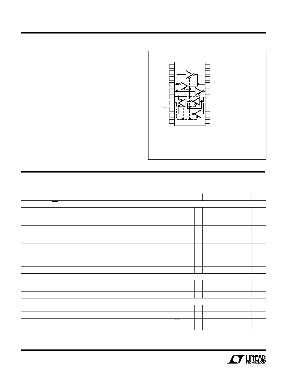
A
U
G
W
A
W
U
W
A
R
BSOLUTE
XI
TI
S
ORDER PART
NUMBER
(Note 1)
Supply Voltage (V
CC
) ............................................. 6.5V
Input Voltage
Drivers ................................... ≠ 0.3V to (V
CC
+ 0.3V)
Receivers ............................................. ≠ 25V to 25V
485/232, ON, DXEN
RXEN, SLEW ........................... ≠ 0.3V to (V
CC
+ 0.3V)
Output Voltage
Drivers ................................................. ≠ 18V to 18V
Receivers ............................... ≠ 0.3V to (V
CC
+ 0.3V)
Short-Circuit Duration
Output ........................................................ Indefinite
V
DD
, V
EE
, C1
+
, C1
≠
, C2
+
, C2
≠
.......................... 30 sec
Operating Temperature Range
LTC1387C .............................................. 0
∞
C to 70
∞
C
LTC1387I ........................................... ≠ 40
∞
C to 85
∞
C
Storage Temperature Range ................ ≠ 65
∞
C to 150
∞
C
Lead Temperature (Soldering, 10 sec)................ 300
∞
C
W
U
U
PACKAGE/ORDER I FOR ATIO
Consult factory for Military grade parts.
T
JMAX
= 125
∞
C,
JA
= 120
∞
C/W (G)
T
JMAX
= 125
∞
C,
JA
= 75
∞
C/W (SW)
1
2
3
4
5
6
7
8
9
10
TOP VIEW
SW PACKAGE
20-LEAD PLASTIC SO
G PACKAGE
20-LEAD PLASTIC SSOP
20
19
18
17
16
15
14
13
12
11
C1
+
C1
≠
V
DD
A
B
Y
Z
485/232
DXEN
GND
C2
+
C2
≠
V
CC
R
A
R
B
D
Y
D
Z
/SLEW
ON
RXEN
V
EE
DC ELECTRICAL CHARACTERISTICS
LTC1387CG
LTC1387CSW
LTC1387IG
LTC1387ISW
T
A
= 25
∞
C, V
CC
= 5V, C1 = C2 = C3 = C4 = 0.1
µ
F (Notes 2, 3), unless otherwise noted.
SYMBOL
PARAMETER
CONDITIONS
MIN
TYP
MAX
UNITS
RS485 Driver (485/232 = High, ON = DXEN = High)
V
OD1
Differential Driver Output Voltage (Unloaded)
I
O
= 0
q
6
V
V
OD2
Differential Driver Output Voltage (With Load)
Figure 1, R = 50
(RS422)
q
2.0
6
V
Figure 1, R = 27
(RS485)
q
1.5
6
V
V
OD
Change in Magnitude of Driver Differential
Figure 1, R = 27
or R = 50
q
0.2
V
Output Voltage for Complementary Output States
V
OC
Driver Common Mode Output Voltage
Figure 1, R = 27
or R = 50
q
3
V
V
OC
Change in Magnitude of Driver Common Mode
Figure 1, R = 27
or R = 50
q
0.2
V
Output Voltage for Complementary Output States
I
OSD
Driver Short-Circuit Current
V
O
= ≠ 7V, 12V; V
O
= High
q
35
250
mA
V
O
= ≠ 7V, 12V; V
O
= Low (Note 4)
q
10
250
mA
I
OZD
Three-State Output Current (Y, Z)
≠ 7V
V
O
12V
±
5
500
µ
A
RS232 Driver (485/232 = Low, ON = DXEN = High)
V
O
Output Voltage Swing
Figure 4, R
L
= 3k, Positive
q
5
6.5
V
Figure 4, R
L
= 3k, Negative
q
≠ 5
≠ 6.5
V
I
OSD
Output Short-Circuit Current
V
O
= 0V
q
±
17
±
60
mA
Driver Inputs and Control Inputs
V
IH
Input High Voltage
D
Y
, D
Z
, DXEN, RXEN, ON, 485/232, SLEW
q
2
V
V
IL
Input Low Voltage
D
Y
, D
Z
, DXEN, RXEN, ON, 485/232, SLEW
q
0.8
V
I
IN
Input Current
D
Y
, D
Z
, DXEN, RXEN, ON, 485/232
q
±
0.1
±
10
µ
A
SLEW (Note 5)
q
5
15
µ
A
3
LTC1387
DC ELECTRICAL CHARACTERISTICS
T
A
= 25
∞
C, V
CC
= 5V, C1 = C2 = C3 = C4 = 0.1
µ
F (Notes 2, 3), unless otherwise noted.
SYMBOL
PARAMETER
CONDITIONS
MIN
TYP
MAX
UNITS
RS485 Receiver (485/232 = High, ON = RXEN = High)
V
TH
Differential Input Threshold Voltage
≠ 7V
V
CM
12V
q
≠ 0.20
0.20
V
V
TH
Input Hysteresis
V
CM
= 0V
40
mV
I
IN
Input Current (A, B)
V
IN
= 12V
q
1
mA
V
IN
= ≠ 7V
q
≠ 0.8
mA
R
IN
Input Resistance
≠ 7V
V
IN
12V
q
12
24
k
RS232 Receiver (485/232 = Low, ON = RXEN = High)
V
TH
Receiver Input Voltage Threshold
Input Low Threshold
q
0.8
V
Input High Threshold
q
2.4
V
V
TH
Receiver Input Hysteresis
0.6
V
R
IN
Receiver Input Resistance
V
IN
=
±
10V
3
5
7
k
Receiver Output (ON = RXEN = High)
V
OH
Receiver Output High Voltage
I
O
= ≠ 3mA, V
IN
= 0V, 485/232 = Low
q
3.5
4.6
V
V
OL
Receiver Output Low Voltage
I
O
= 3mA, V
IN
= 3V, 485/232 = Low
q
0.2
0.4
V
I
OSR
Short-Circuit Current
0V
V
O
V
CC
q
7
85
mA
I
OZR
Three-State Output Current
RXEN = 0V
q
±
0.1
±
10
µ
A
Power Supply Generator
V
DD
V
DD
Output Voltage
No Load, ON = DXEN = RXEN = High
8
V
I
DD
= ≠ 5mA, ON = DXEN = RXEN = High
7
V
V
EE
V
EE
Output Voltage
No Load, ON = DXEN = RXEN = High
≠ 7.7
V
I
EE
= 5mA, ON = DXEN = RXEN = High
≠ 7.0
V
Power Supply
I
CC
V
CC
Supply Current
No Load, ON = DXEN = RXEN = High
q
7
25
mA
Shutdown, ON = DXEN = RXEN = 0V
q
5
100
µ
A
AC ELECTRICAL CHARACTERISTICS
T
A
= 25
∞
C, V
CC
= 5V, C1 = C2 = C3 = C4 = 0.1
µ
F (Notes 2, 3), unless otherwise noted.
SYMBOL
PARAMETER
CONDITIONS
MIN
TYP
MAX
UNITS
RS232 Mode (ON = DXEN = RXEN = High, 485/232 = Low)
SR
Slew Rate
Figure 4, R
L
= 3k, C
L
= 15pF
q
30
V/
µ
s
Figure 4, R
L
= 3k, C
L
= 1000pF
q
4
V/
µ
s
t
T
Transition Time
Figure 4, R
L
= 3k, C
L
= 2500pF
q
0.22
1.9
3.1
µ
s
t
PLH
Driver Input to Output
Figures 4, 10, R
L
= 3k, C
L
= 15pF
q
0.6
4
µ
s
t
PHL
Driver Input to Output
Figures 4, 10, R
L
= 3k, C
L
= 15pF
q
0.6
4
µ
s
t
PLH
Receiver Input to Output
Figures 5, 11
q
0.3
6
µ
s
t
PHL
Receiver Input to Output
Figures 5, 11
q
0.4
6
µ
s
RS485 Mode (Fast Slew Rate, ON = DXEN = High, 485/232 = High, SLEW = High)
t
PLH
Driver Input to Output
Figures 2, 7, R
L
= 54
, C
L
= 100pF
q
15
40
70
ns
t
PHL
Driver Input to Output
Figures 2, 7, R
L
= 54
, C
L
= 100pF
q
15
40
70
ns
t
SKEW
Driver Output to Output
Figures 2, 7, R
L
= 54
, C
L
= 100pF
q
5
15
ns
t
r
, t
f
Driver Rise or Fall Time
Figures 2, 7, R
L
= 54
, C
L
= 100pF
q
3
15
40
ns

4
LTC1387
AC ELECTRICAL CHARACTERISTICS
T
A
= 25
∞
C, V
CC
= 5V, C1 = C2 = C3 = C4 = 0.1
µ
F (Notes 2, 3), unless otherwise noted.
The
q
denotes specifications which apply over the full operating
temperature range.
Note 1: Absolute Maximum Ratings are those values beyond which the life
of the device may be impaired.
Note 2: All currents into device pins are positive; all currents out of device
pins are negative. All voltages are referenced to device ground unless
otherwise specified.
Note 3: All typicals are given at V
CC
= 5V, C1 = C2 = C3 = C4 = 0.1
µ
F
and T
A
= 25
∞
C.
Note 4: Short-circuit current for RS485 driver output low state folds back
above V
CC
. Peak current occurs around V
O
= 3V.
Note 5: SLEW includes an internal pull-up in RS485 mode.
PI
N
FU
N
CTIO
N
S
U
U
U
C1
+
(Pin 1): Commutating Capacitor C1 Positive Terminal.
Requires an external 0.1
µ
F capacitor between Pins 1 and 2.
C1
≠
(Pin 2): Commutating Capacitor C1 Negative Terminal.
V
DD
(Pin 3): Charge Pump Positive Supply Output.
Requires an external 0.1
µ
F capacitor to ground.
A (Pin 4): Receiver Input A. Inverting input of RS232
receiver A in RS232 mode; inverting RS485 receiver input
in RS485 mode.
B (Pin 5): Receiver Input B. Inverting input of RS232
receiver B in RS232 mode; noninverting RS485 receiver
input in RS485 mode.
Y (Pin 6): Driver Output Y. Inverting RS232 driver Y output
in RS232 mode; inverting RS485 driver output in RS485
mode.
Z (Pin 7): Driver Output Z. Inverting RS232 driver Z output
in RS232 mode; noninverting RS485 driver output in
RS485 mode.
SYMBOL
PARAMETER
CONDITIONS
MIN
TYP
MAX
UNITS
RS485 Mode (Fast Slew Rate, ON = DXEN = High, 485/232 = High, SLEW = High)
t
ZL
Driver Enable to Output Low
Figures 3, 8, C
L
= 100pF, S1 Closed
q
50
90
ns
t
ZH
Driver Enable to Output High
Figures 3, 8, C
L
= 100pF, S2 Closed
q
50
90
ns
t
LZ
Driver Disable from Low
Figures 3, 8, C
L
= 15pF, S1 Closed
q
50
90
ns
t
HZ
Driver Disable from High
Figures 3, 8, C
L
= 15pF, S2 Closed
q
60
90
ns
RS485 Mode (Slow Slew Rate, ON = DXEN = High, 485/232 = High, SLEW = Low)
t
PLH
Driver Input to Output
Figures 2, 7, R
L
= 54
, C
L
= 100pF
q
100
700
1500
ns
t
PHL
Driver Input to Output
Figures 2, 7, R
L
= 54
, C
L
= 100pF
q
100
700
1500
ns
t
SKEW
Driver Output to Output
Figures 2, 7, R
L
= 54
, C
L
= 100pF
q
200
750
ns
t
r
, t
f
Driver Rise or Fall Time
Figures 2, 7, R
L
= 54
, C
L
= 100pF
q
150
300
1500
ns
t
ZL
Driver Enable to Output Low
Figures 3, 8, C
L
= 100pF, S1 Closed
q
600
1500
ns
t
ZH
Driver Enable to Output High
Figures 3, 8, C
L
= 100pF, S2 Closed
q
600
1500
ns
t
LZ
Driver Disable from Low
Figures 3, 8, C
L
= 15pF, S1 Closed
q
100
200
ns
t
HZ
Driver Disable from High
Figures 3, 8, C
L
= 15pF, S2 Closed
q
100
200
ns
RS485 Mode (ON = RXEN = High, 485/232 = High)
t
PLH
Receiver Input to Output
Figures 2, 9, R
L
= 54
, C
L
= 100pF
q
20
70
140
ns
t
PHL
Receiver Input to Output
Figures 2, 9, R
L
= 54
, C
L
= 100pF
q
20
70
140
ns
t
SKEW
Differential Receiver Skew,
t
PLH
≠ t
PHL
Figures 2, 9, R
L
= 54
, C
L
= 100pF
10
ns
Receiver Output Enable/Disable (ON = High)
t
ZL
Receiver Enable to Output Low
Figures 6, 12, C
L
= 15pF, S1 Closed
q
40
90
ns
t
ZH
Receiver Enable to Output High
Figures 6, 12, C
L
= 15pF, S2 Closed
q
40
90
ns
t
LZ
Receiver Disable from Low
Figures 6, 12, C
L
= 15pF, S1 Closed
q
40
90
ns
t
HZ
Receiver Disable from High
Figures 6, 12, C
L
= 15pF, S2 Closed
q
40
90
ns

5
LTC1387
PI FU CTIO S
U
U
U
485/232 (Pin 8): Interface Mode Select Input. A low logic
input enables two RS232 drivers and two RS232 receiv-
ers. A high input enables the RS485 driver and the RS485
receiver.
DXEN (Pin 9): Driver Enable Input. A high logic input
enables the drivers and a low logic input disables the
drivers. When disabled, all driver outputs are in high
impedance
GND (Pin 10): Ground.
V
EE
(Pin 11): Charge Pump Negative Supply Output.
Requires an external 0.1
µ
F capacitor to ground.
RXEN (Pin 12): Receiver Enable Input. A high logic input
enables the receivers and a low logic input disables the
receivers. When disabled, all receiver outputs are in high
impedance.
ON (Pin 13): A high logic level at ON input keeps the charge
pump active regardless of the state of the DXEN and RXEN
inputs. When the charge pump is active, the drivers and
receivers can be enabled or disabled without waiting for
charge pump stabilization time (typically 100
µ
s with 0.1
µ
F
capacitors). A low logic state at the ON, DXEN and RXEN
inputs will put the transceiver and charge pump in shut-
down mode and reduces I
CC
to 5
µ
A. Whenever the trans-
ceiver is activated from shutdown, the charge pump
should be allowed to stabilize before data transmission.
When DXEN and RXEN are high and ON is low, the charge
pump, drivers and receivers are all active and the driver
outputs are internally looped back to the inputs of the
receiver. The three control inputs ON, DXEN and RXEN can
be configured for one-, two- or three-wire control: one-
wire mode ≠ all three inputs connected together; two-wire
mode ≠ inputs ON and RXEN connected to one wire, DXEN
a separate wire; three-wire mode ≠ separate wires to each
input. See the Function Tables.
D
Z
/SLEW (Pin 14): Driver Z or Slew Input. In RS232
mode, this pin is the driver Z input. In RS485 mode, this
pin controls the slew rate of the RS485 driver. With the
SLEW pin high, the RS485 driver runs at maximum (fast)
slew rate and can transmit signals up to 5MBd. With the
SLEW pin low, the RS485 driver runs with reduced (slow)
slew rate to control reflections with improperly terminated
cables. In slow mode, the RS485 driver can support data
rates up to 150kBd. This SLEW pin has internal 5
µ
A pull-
up during RS485 mode.
D
Y
(Pin 15): Driver Y Input. Input Y in RS232 mode; the
differential driver input in RS485 mode.
R
B
(Pin 16): Receiver B Output. Output B in RS232 mode;
output is high impedance in RS485 mode.
R
A
(Pin 17): Receiver A Output. Output A in RS232 mode;
the differential receiver output in RS485 mode.
V
CC
(Pin 18): Positive Supply. 4.75V
V
CC
5.25V.
Requires an external 0.1
µ
F bypass capacitor to ground.
C2
≠
(Pin 19): Commutating Capacitor C2 Negative Termi-
nal. Requires an external 0.1
µ
F capacitor between Pins 19
and 20.
C2
+
(Pin 20): Commutating Capacitor C2 Positive
Terminal.