1408f.pm65
1
LTC1408
1408f
6 Channel, 14-Bit, 600ksps
Simultaneous Sampling ADC
with Shutdown
The LTC
®
1408 is a 14-bit, 600ksps ADC with six simulta-
neously sampled differential inputs. The device draws
only 5mA from a single 3V supply, and comes in a tiny 32
pin (5mm
× 5mm) QFN package. A SLEEP shutdown
feature lowers power consumption to 6
µW. The combina-
tion of low power and tiny package makes the LTC1408
suitable for portable applications.
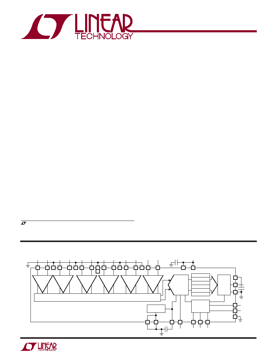
The LTC1408 contains six separate differential inputs that
are sampled simultaneously on the rising edge of the
CONV signal. These six sampled inputs are then
converted at a rate of 100ksps per channel.
The 90dB common mode rejection allows users to
eliminate ground loops and common mode noise by
measuring signals differentially from the source.
The device converts 0V to 2.5V unipolar inputs differen-
tially, or
±1.25V bipolar inputs also differentially,
depending on the state of the BIP pin. Any analog input
may swing rail-to-rail as long as the differential input
range is maintained.
The conversion sequence can be abbreviated to convert
fewer than six channels, depending on the logic state of
the SEL2, SEL1 and SEL0 inputs.
The serial interface sends out the six conversion results in
96 clocks for compatibility with standard serial interfaces.
600ksps ADC with 6 Simultaneously Sampled
Differential Inputs
100ksps Throughput per Channel
76dB SINAD
Low Power Dissipation: 15mW
3V Single Supply Operation
2.5V Internal Bandgap Reference, Can be Overdriven
with External Reference
3-Wire Serial Interface
Internal Conversion Triggered by CONV
SLEEP (6
µW) Shutdown Mode
NAP (3.3mW) Shutdown Mode
0V to 2.5V Unipolar, or
±1.25V Bipolar Differential
Input Range
90dB Common Mode Rejection
Tiny 32-Pin (5mm
××
××
×
5mm) QFN Package
Multiphase Power Measurement
Multiphase Motor Control
Data Acquisition Systems
Uninterruptable Power Supplies
APPLICATIO S
U
FEATURES
DESCRIPTIO
U
BLOCK DIAGRA
W
, LTC and LT are registered trademarks of Linear Technology Corporation. All other
trademarks are the property of their respective owners. Protected by U.S. Patents including
6084440, 6522187.
+
4
5
25
24
+
7
6
9
12
13
16
19
8
CH0
CH0
+
CH1
CH1
+
10
11
+
14
15
CH2
CH2
+
CH3
CH3
+
+
17
18
+
20
21
S AND H
S AND H
S AND H
S AND H
S AND H
CH4
CH4
+
CH5
CH5
+
MUX
V
REF
10
µF
BIP
SEL2 SEL1 SEL0
GND
2.5V
REFERENCE
600ksps
14-BIT ADC
14-BIT LATCH 5
14-BIT LATCH 4
14-BIT LATCH 3
14-BIT LATCH 2
14-BIT LATCH 1
14-BIT LATCH 0
10
µF
3V
V
CC
V
DD
26
29
23
22
33
27
28
2
1
SD0
0.1
µF
3
OV
DD
3V
32
SCK
31
DGND
OGND
30
CONV
THREE-
STATE
SERIAL
OUTPUT
PORT
TIMING
LOGIC
1408 TA01
+
S AND H
2
LTC1408
1408f
A
U
G
W
A
W
U
W
A
R
BSOLUTE
XI
TI
S
(Notes 1, 2)
Supply Voltage (V
DD
, V
CC
, OV
DD
) .............................. 4V
Analog Input Voltage
(Note 3) ................................... 0.3V to (V
DD
+ 0.3V)
Digital Input Voltage .................... 0.3V to (V
DD
+ 0.3V)
Digital Output Voltage .................. 0.3V to (V
DD
+ 0.3V)
Power Dissipation .............................................. 100mW
Operation Temperature Range
LTC1408C ............................................... 0
°C to 70°C
LTC1408I ............................................ 40
°C to 85°C
Storage Temperature Range ................. 65
°C to 125°C
The
denotes the specifications which apply over the full operating
temperature range, otherwise specifications are at T
A
= 25
°C. With internal reference, V
DD
= 3V, V
DD
= V
CC
= 3V.
PARAMETER
CONDITIONS
MIN
TYP
MAX
UNITS
Resolution (No Missing Codes)
14
Bits
Integral Linearity Error
(Note 5)
3
±0.5
3
LSB
Offset Error
(Note 4)
4.5
±1
4.5
mV
Offset Match from CH0 to CH5
3
±0.5
3
mV
Range Error
(Note 4)
12
±2
12
mV
Range Match from CH0 to CH5
5
±1
5
mV
Range Tempco
Internal Reference (Note 4)
±15
ppm/
°C
External Reference
±1
ppm/
°C
The
denotes the specifications which apply over the full operating temperature range,
otherwise specifications are at T
A
= 25
°C. With internal reference, V
DD
= 3V, V
DD
= V
CC
= 3V.
SYMBOL
PARAMETER
CONDITIONS
MIN
TYP
MAX
UNITS
V
IN
Analog Differential Input Range (Notes 3, 8, 9)
2.7V
V
DD
3.3V
0 to 2.5
V
V
CM
Analog Common Mode + Differential
0 to V
DD
V
Input Range
(Note 8)
I
IN
Analog Input Leakage Current
1
µA
C
IN
Analog Input Capacitance
13
pF
t
ACQ
Sample-and-Hold Acquisition Time
(Note 6)
39
ns
t
AP
Sample-and-Hold Aperture Delay Time
1
ns
t
JITTER
Sample-and-Hold Aperture Delay Time Jitter
0.3
ps
t
SK
Channel to Channel Aperture Skew
200
ps
CMRR
Analog Input Common Mode Rejection Ratio
f
IN
= 100kHz, V
IN
= 0V to 3V
83
dB
f
IN
= 10MHz, V
IN
= 0V to 3V
67
dB
CO VERTER CHARACTERISTICS
U
A ALOG I PUT
U
U
W
U
U
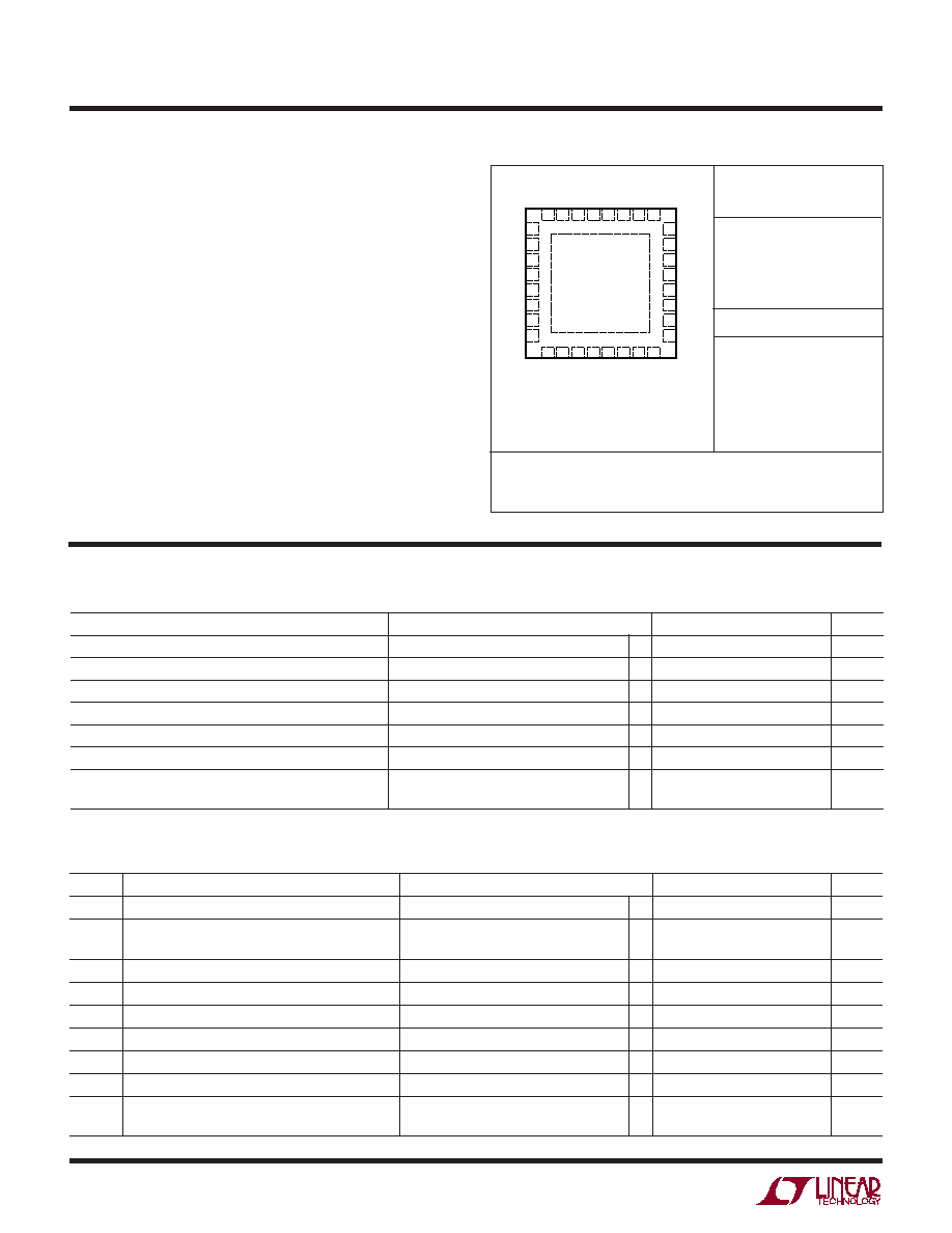
PACKAGE/ORDER I FOR ATIO
ORDER PART
NUMBER
QFN PART MARKING
T
JMAX
= 125
°C,
JA
= 34
°C/ W
EXPOSED PIN IS GND (PAD 33)
MUST BE SOLDERED TO PCB
Consult LTC Marketing for parts specified with wider operating temperature ranges.
16 15 14 13 12 11 10
9
25 26 27 28
TOP VIEW
QFN PACKAGE
32-PIN (5mm
× 5mm) PLASTIC QFN
29 30 31 32
1
2
3
4
5
6
7
8
24
23
22
21
20
19
18
17
CH4
+
CH4
GND
CH5
+
CH5
GND
V
REF
V
CC
CH1
CH1
+
GND
CH0
CH0
+
OV
DD
OGND
SDO
GND
CH3
CH3
+
GND
GND
CH2
CH2
+
GND
V
DD
SEL2
SEL1
SEL0
BIP
CONV
DGND
SCK
33
LTC1408CUH
LTC1408IUH
1408
Order Options Tape and Reel: Add #TR
Lead Free: Add #PBF Lead Free Tape and Reel: Add #TRPBF
Lead Free Part Marking:
http://www.linear.com/leadfree/
3
LTC1408
1408f
I TER AL REFERE CE CHARACTERISTICS
U
U
U
The
denotes the specifications which apply over the full operating temperature range,
otherwise specifications are at T
A
= 25
°C. With internal reference, V
DD
= 3V, V
DD
= V
CC
= 3V.
SYMBOL
PARAMETER
CONDITIONS
MIN
TYP
MAX
UNITS
SINAD
Signal-to-Noise Plus
100kHz Input Signal
73
76
dB
Distortion Ratio
300kHz Input Signal
76
dB
100kHz Input Signal, External V
REF
= 3.3V, V
DD
3.3V
79
dB
300kHz Input Signal, External V
REF
= 3.3V, V
DD
3.3V
79
dB
THD
Total Harmonic
100kHz First 5 Harmonics
80
90
dB
Distortion
300kHz First 5 Harmonics
86
dB
SFDR
Spurious Free
100kHz Input Signal
90
dB
Dynamic Range
300kHz Input Signal
86
dB
IMD
Intermodulation
0.625V
P-P
, 833kHz into CH0+, 0.625V
P-P
, 841kHz into CH0.
80
dB
Distortion
Bipolar Mode. Also Applicable to Other Channels
Code-to-Code
V
REF
= 2.5V (Note 17)
0.7
LSB
RMS
Transition Noise
Full Power Bandwidth
V
IN
= 2.5V
P-P
, SDO = 11585LSB
P-P
(3dBFS) (Note 15)
50
MHz
Full Linear Bandwidth
S/(N + D)
68dB, Bipolar Differential Input
5
MHz
T
A
= 25
°C. V
DD
= V
CC
= 3V.
PARAMETER
CONDITIONS
MIN
TYP
MAX
UNITS
V
REF
Output Voltage
I
OUT
= 0
2.5
V
V
REF
Output Tempco
15
ppm/
°C
V
REF
Line Regulation
V
DD
= 2.7V to 3.6V, V
REF
= 2.5V
600
µV/V
V
REF
Output Resistance
Load Current = 0.5mA
0.2
V
REF
Settling Time
2
ms
The
denotes the specifications which apply over the
full operating temperature range, otherwise specifications are at T
A
= 25
°C. V
DD
= V
CC
= 3V.
SYMBOL
PARAMETER
CONDITIONS
MIN
TYP
MAX
UNITS
V
IH
High Level Input Voltage
V
DD
= 3.3V
2.4
V
V
IL
Low Level Input Voltage
V
DD
= 2.7V
0.6
V
I
IN
Digital Input Current
V
IN
= 0V to V
DD
±10
µA
C
IN
Digital Input Capacitance
5
pF
V
OH
High Level Output Voltage
V
DD
= 3V, I
OUT
= 200
µA
2.5
2.9
V
V
OL
Low Level Output Voltage
V
DD
= 2.7V, I
OUT
= 160
µA
0.05
V
V
DD
= 2.7V, I
OUT
= 1.6mA
0.4
V
I
OZ
Hi-Z Output Leakage D
OUT
V
OUT
= 0V and V
DD
±10
µA
C
OZ
Hi-Z Output Capacitance D
OUT
1
pF
I
SOURCE
Output Short-Circuit Source Current
V
OUT
= 0V, V
DD
= 3V
20
mA
I
SINK
Output Short-Circuit Sink Current
V
OUT
= V
DD
= 3V
15
mA
DY
A
IC ACCURACY
U
W
DIGITAL I PUTS A D DIGITAL OUTPUTS
U
U
4
LTC1408
1408f
SYMBOL
PARAMETER
CONDITIONS
MIN
TYP
MAX
UNITS
f
SAMPLE(MAX)
Maximum Sampling Frequency per Channel
100
kHz
(Conversion Rate)
t
THROUGHPUT
Minimum Sampling Period (Conversion + Acquisiton Period)
667
ns
t
SCK
Clock Period
(Note 16)
100
10000
ns
t
CONV
Conversion Time
(Notes 6, 17)
96
SCLK cycles
t
1
Minimum Positive or Negative SCLK Pulse Width
(Note 6)
2
ns
t
2
CONV to SCK
Setup Time
(Notes 6, 10)
3
10000
ns
t
3
SCK
Before CONV
(Note 6)
0
ns
t
4
Minimum Positive or Negative CONV Pulse Width
(Note 6)
4
ns
t
5
SCK to Sample Mode
(Note 6)
4
ns
t
6
CONV to Hold Mode
(Notes 6, 11)
1.2
ns
t
7
96th SCK
to CONV Interval (Affects Acquisition Period)
(Notes 6, 7, 13)
45
ns
t
8
Minimum Delay from SCK
to Valid Bits 0 Through 11
(Notes 6, 12)
8
ns
t
9
SCK to Hi-Z at SDO
(Notes 6, 12)
6
ns
t
10
Previous SDO Bit Remains Valid After SCK
(Notes 6, 12)
2
ns
t
11
V
REF
Settling Time After Sleep-to-Wake Transition
(Notes 6, 14)
2
ms
The
denotes the specifications which apply over the full operating temperature
range, otherwise specifications are at T
A
= 25
°C. With internal reference, V
DD
= V
CC
= 3V.
SYMBOL
PARAMETER
CONDITIONS
MIN
TYP
MAX
UNITS
V
DD
, V
CC
Supply Voltage
2.7
3.6
V
I
DD
+ I
CC
Supply Current
Active Mode, f
SAMPLE
= 600ksps
5
7
mA
Nap Mode
1.1
1.9
mA
Sleep Mode
2.0
15
µA
PD
Power Dissipation
Active Mode with SCK, f
SAMPLE
= 600ksps
15
mW
POWER REQUIRE E TS
W
U
The
denotes the specifications which apply over the full operating temperature
range, otherwise specifications are at T
A
= 25
°C. V
DD
= 3V.
TI I G CHARACTERISTICS
U
W
Note 1: Stresses beyond those listed under Absolute Maximum Ratings
may cause permanent damage to the device. Exposure to any Absolute
Maximum Rating condition for extended periods may affect device
reliabilty and lifetime.
Note 2: All voltage values are with respect to ground GND.
Note 3: When these pins are taken below GND or above V
DD
, they will be
clamped by internal diodes. This product can handle input currents greater
than 100mA below GND or greater than V
DD
without latchup.
Note 4: Offset and range specifications apply for a single-ended CH0
+
CH5
+
input with CH0
CH5
grounded and using the internal 2.5V
reference.
Note 5: Integral linearity is tested with an external 2.55V reference and is
defined as the deviation of a code from the straight line passing through
the actual endpoints of a transfer curve. The deviation is measured from
the center of quantization band. Linearity is tested for CH0 only.
Note 6: Guaranteed by design, not subject to test.
Note 7: Recommended operating conditions.
Note 8: The analog input range is defined for the voltage difference
between CHx
+
and CHx
, x = 05.
Note 9: The absolute voltage at CHx
+
and CHx
must be within this range.
Note 10: If less than 3ns is allowed, the output data will appear one clock
cycle later. It is best for CONV to rise half a clock before SCK, when
running the clock at rated speed.
Note 11: Not the same as aperture delay. Aperture delay (1ns) is the
difference between the 2.2ns delay through the sample-and-hold and the
1.2ns CONV to Hold mode delay.
Note 12: The rising edge of SCK is guaranteed to catch the data coming
out into a storage latch.
Note 13: The time period for acquiring the input signal is started by the
96th rising clock and it is ended by the rising edge of CONV.
Note 14: The internal reference settles in 2ms after it wakes up from Sleep
mode with one or more cycles at SCK and a 10
µF capacitive load.
Note 15: The full power bandwidth is the frequency where the output code
swing drops by 3dB with a 2.5V
P-P
input sine wave.
Note 16: Maximum clock period guarantees analog performance during
conversion. Output data can be read with an arbitrarily long clock period.
Note 17: The conversion process takes 16 clocks for each channel that is
enabled, up to 96 clocks for all 6 channels.
5
LTC1408
1408f
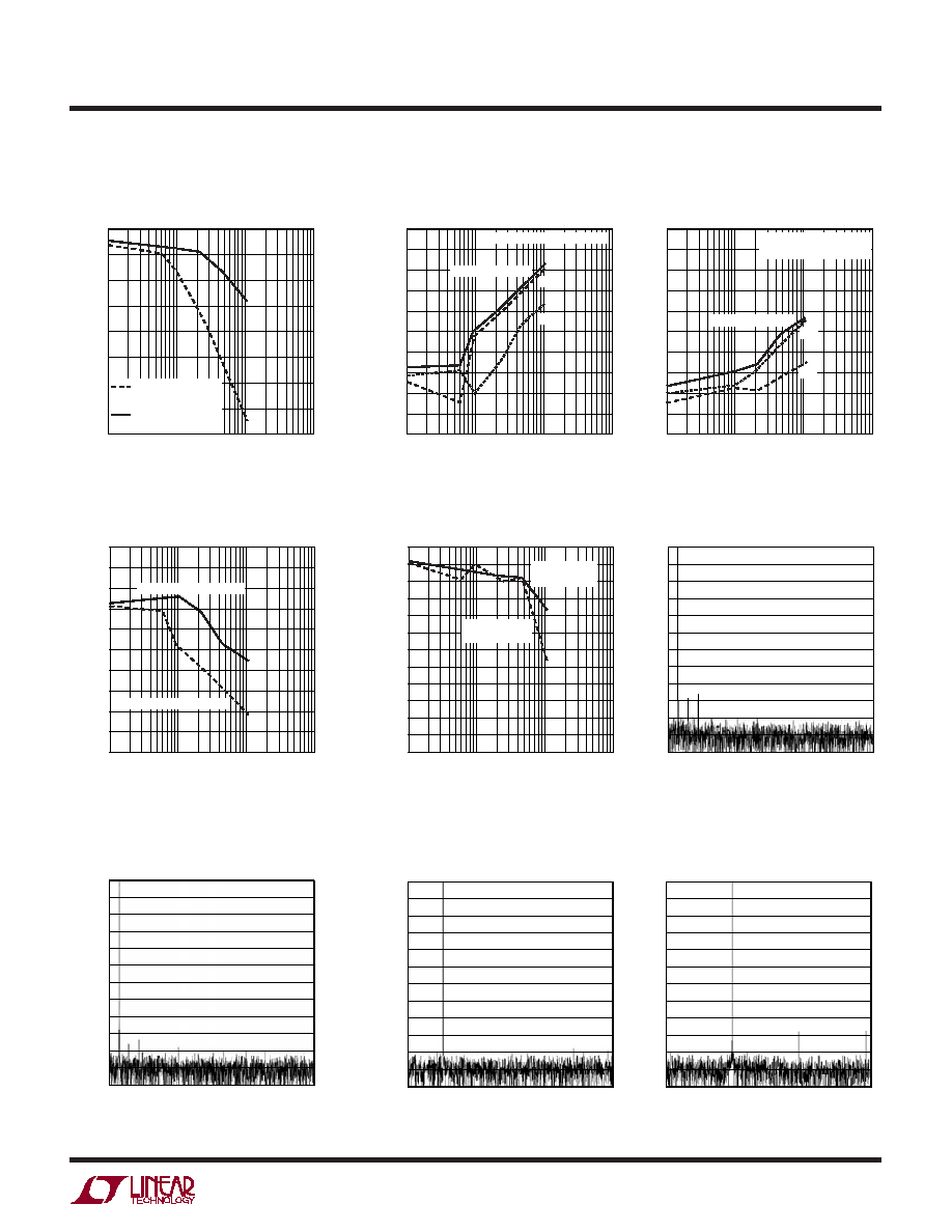
SINAD, ENOBs vs Frequency
SFDR vs Input Frequency
V
DD
= 3V, T
A
= 25
°C
THD, 2nd and 3rd
vs Input Frequency
TYPICAL PERFOR A CE CHARACTERISTICS
U
W
98kHz Unipolar Sine Wave 4096
Point FFT Plot, 100 ksps
98kHz Bipolar Sine Wave 4096
Point FFT Plot, 100 ksps
SNR vs Input Frequency
THD, 2nd and 3rd
vs Input Frequency
FREQUENCY (MHz)
56
SINAD (dB)
ENOBS (bits)
59
62
65
68
71
74
77
1
10
100
1408 G01
53
9
9.5
10
10.5
11
11.5
12
12.5
8.5
0.1
UNIPOLAR SINGLE
ENDED
BIPOLAR
DIFFERENTIAL
FREQUENCY (MHz)
98
THD (dB)
92
74
80
86
68
62
56
50
44
1
10
100
1408 G02
104
0.1
5 HARMONIC THD
UNIPOLAR SINGLE ENDED
2nd
3rd
FREQUENCY (MHz)
98
THD (dB)
92
74
80
86
68
62
56
50
44
1
10
100
1408 G03
104
0.1
5 HARMONIC THD
BIPOLAR SINGLE ENDED
V
CM
= 1.5V
2nd
3rd
FREQUENCY (MHz)
50
SFDR (dB)
56
74
68
62
80
86
92
98
104
1
10
100
1408 G04
44
0.1
UNIPOLAR SINGLE ENDED
BIPOLAR DIFFERENTIAL
FREQUENCY (MHz)
65
SNR (dB)
66
69
68
67
70
71
72
75
74
73
76
1
10
100
1408 G05
64
0.1
UNIPOLAR
SINGLE ENDED
BIPOLAR
DIFFERENTIAL
FREQUENCY(kHz)
0
120
OUTPUT MAGNITUDE (dB)
80
90
100
110
40
60
70
50
0
10
20
30
10
30
20
1408 G06
40
50
FREQUENCY(kHz)
0
120
OUTPUT MAGNITUDE (dB)
80
90
100
110
40
60
70
50
0
10
20
30
10
30
20
1408 G07
40
50
591kHz Bipolar Differential Sine
Wave 4096 Point FFT Plot,
100 ksps
101kHz Unipolar Single Ended
Sine Wave 4096 Point FFT Plot,
625 ksps
FREQUENCY(kHz)
0
120
OUTPUT MAGNITUDE (dB)
80
90
100
110
40
60
70
50
0
10
20
30
10
30
20
1408 G08
40
50
FREQUENCY(kHz)
0
120
OUTPUT MAGNITUDE (dB)
80
90
100
110
40
60
70
50
0
10
20
30
62.5
188
125
1408 G09
250
313