Äîêóìåíòàöèÿ è îïèñàíèÿ www.docs.chipfind.ru
1
LTC1480
3.3V Ultra-Low Power
RS485 Transceiver
S
FEATURE
D
U
ESCRIPTIO
The LTC
®
1480 is an ultra-low power differential line trans-
ceiver which provides full RS485 compatibility while oper-
ating from a single 3.3V supply. It is designed for data
transmission standard RS485 applications with extended
common-mode range (12V to 7V). It also meets the
requirements of RS422 and features high speed operation
up to 2.5Mb/s. The CMOS design offers significant power
savings without sacrificing ruggedness against overload
or ESD damage. Typical quiescent current is only 300
µ
A
while operating and 1
µ
A in shutdown.
The driver and receiver feature three-state outputs, with
the driver outputs maintaining high impedance over the
entire common-mode range. Excessive power dissipation
caused by bus contention or faults is prevented by a
thermal shutdown circuit which forces the driver outputs
into a high impedance state. The receiver has a fail-safe
feature which guarantees a high output state when the
inputs are left open. I/O pins are protected against multiple
ESD strikes of up to
±
10kV.
The LTC1480 is fully specified over the commercial and
extended industrial temperature range. The LTC1480 is
available in 8-pin SO and DIP packages.
s
True RS485 from a Single 3.3V Supply
s
Low Power: I
CC
= 500
µ
A Max with Driver Disabled
s
I
CC
= 600
µ
A Max with Driver Enabled, No Load
s
1
µ
A Quiescent in Shutdown Mode
s
ESD Protection to
±
10kV on Receiver Inputs and
Driver Outputs
s
7V to 12V Common-Mode Range Permits
±
7V
Ground Difference Between Devices on the Data Line
s
Thermal Shutdown Protection
s
Power Up/Down Glitch-Free Driver Outputs Permit
Live Insertion or Removal of Transceiver
s
Driver Maintains High Impedance in Three-State or
with the Power Off
s
Up to 32 Transceivers on the Bus
s
50ns Typical Driver Propagation Delays with
10ns Skew
s
Pin Compatible with the LTC485
, LTC and LT are registered trademarks of Linear Technology Corporation.
s
Battery-Powered RS485/RS422 Applications
s
Low Power RS485/RS422 Transceiver
s
Level Translator
U
S
A
O
PPLICATI
U
A
O
PPLICATI
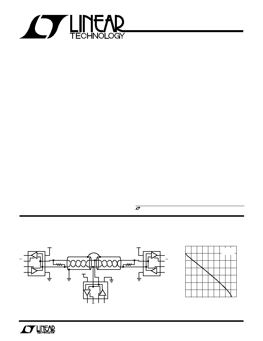
TYPICAL
Driver Differential
Output Voltage vs Output Current
3.3V RS485 Network
RO
RE
DE
D1
1
2
3
4
8
7
6
5
LTC1480 · TA01
LTC1480
LTC1480
A
A
B
B
A
B
120
120
SHIELD
SHIELD
R
D
3.3V
RO
RE
DE
D1
1
2
3
4
8
7
6
5
LTC1480
R
D
3.3V
3.3V
R
D
1
2
3
4
8
7
6
5
RO
RE
DE D1
OUTPUT CURRENT (mA)
0
0
OUTPUT VOLTAGE (V)
0.5
1.0
1.5
2.0
2.5
60
70
80
LTC1480 · TA02
10
20
30
40
50
90
3.0
3.5
V
CC
= 3.3V
T
A
= 25
°
C
2
LTC1480
A
U
G
W
A
W
U
W
A
R
BSOLUTE
XI
TI
S
W
U
U
PACKAGE/ORDER I FOR ATIO
(Note 1)
Supply Voltage (V
CC
) ................................................ 7V
Control Input Voltage ..................... 0.3V to V
CC
+ 0.3V
Driver Input Voltage ....................... 0.3V to V
CC
+ 0.3V
Driver Output Voltage ...........................................
±
14V
Receiver Input Voltage ..........................................
±
14V
Receiver Output Voltage ................ 0.3V to V
CC
+ 0.3V
Operating Temperature Range
LTC1480C ........................................ 0
°
C
T
A
70
°
C
LTC1480I .................................... 40
°
C
T
A
85
°
C
Storage Temperature Range ................. 65
°
C to 150
°
C
Lead Temperature (Soldering, 10 sec) .................. 300
°
C
1480
1480I
LTC1480CN8
LTC1480IN8
LTC1480CS8
LTC1480IS8
S8 PART MARKING
ORDER PART
NUMBER
T
JMAX
= 125
°
C,
JA
= 130
°
C/ W (N8)
T
JMAX
= 125
°
C,
JA
= 150
°
C/ W (S8)
Consult factory for Military grade parts.
SYMBOL
PARAMETER
CONDITIONS
MIN
TYP
MAX
UNITS
V
OD1
Differential Driver Output Voltage (Unloaded)
I
O
= 0V
q
3.3
V
V
OD2
Differential Driver Output Voltage (with Load)
R = 27
(RS485), Figure 1
q
1.5
3.3
V
R = 50
(RS422)
q
2.0
V
V
OD
Change in Magnitude of Driver Differential Output
R = 27
or R = 50
, Figure 1
q
0.2
V
Voltage for Complementary Output States
V
OC
Driver Common-Mode Output Voltage
R = 27
or R = 50
, Figure 1
q
2
V
V
OC
Change in Magnitude of Driver Common-Mode
R = 27
or R = 50
, Figure 1
q
0.2
V
Output Voltage for Complementary Output States
V
IH
Input HIGH Voltage
DE, DI, RE
q
2
V
V
IL
Input LOW Voltage
DE, DI, RE
q
0.8
V
I
IN1
Input Current
DE, DI, RE
q
±
2
µ
A
I
IN2
Input Current (A, B)
DE = 0, V
CC
= 0V or 3.6V, V
IN
= 12V
q
1.0
mA
DE = 0, V
CC
= 0V or 3.6V, V
IN
= 7V
q
0.8
mA
V
TH
Differential Input Threshold Voltage for Receiver
7V
V
CM
12V
q
0.2
0.2
V
V
TH
Receiver Input Hysteresis
V
CM
= 0V
70
mV
V
OH
Receiver Output HIGH Voltage
I
O
= 4mA, V
ID
= 200mV
q
2
V
V
OL
Receiver Output LOW Voltage
I
O
= 4mA, V
ID
= 200mV
q
0.4
V
I
OZR
Three-State (High Impedance) Output
V
CC
= Max, 0.4V
V
O
2.4V
q
±
1
µ
A
Current at Receiver
R
IN
Receiver Input Resistance
7V
V
CM
12V
q
12
k
I
CC
Supply Current
No Load, Output Enabled
q
400
600
µ
A
No Load, Output Disabled
q
300
500
µ
A
I
SHDN
Supply Current in Shutdown Mode
DE = 0, RE = V
CC
1
10
µ
A
I
OSD1
Driver Short-Circuit Current, V
OUT
= HIGH
7V
V
O
12V
q
35
250
mA
I
OSD2
Driver Short-Circuit Current, V
OUT
= LOW
7V
V
O
12V
q
35
250
mA
I
OSR
Receiver Short-Circuit Current
0V
V
O
V
CC
q
7
85
mA
ELECTRICAL C
C
HARA TERISTICS
V
CC
= 3.3V (Notes 2, 3)
1
2
3
4
8
7
6
5
TOP VIEW
V
CC
B
A
GND
N8 PACKAGE
8-LEAD PDIP
S8 PACKAGE
8-LEAD PLASTIC SO
R
D
RO
RE
DE
DI
3
LTC1480
SYMBOL
PARAMETER
CONDITIONS
MIN
TYP
MAX
UNITS
t
PLH
Driver Input to Output
R
DIFF
= 54
, C
L1
= C
L2
= 100pF,
q
25
50
80
ns
(Figures 3 and 5)
t
PHL
Driver Input to Output
q
25
50
80
t
SKEW
Driver Output to Output
q
10
20
t
R
, t
F
Driver Rise or Fall Time
q
5
15
40
t
ZH
Driver Enable to Output HIGH
C
L
= 100pF (Figures 4, 6), S2 Closed
q
70
120
ns
t
ZL
Driver Enable to Output LOW
C
L
= 100pF (Figures 4, 6), S1 Closed
q
70
120
ns
t
LZ
Driver Disable Time from LOW
C
L
= 15pF (Figures 4, 6), S1 Closed
q
70
120
ns
t
HZ
Driver Disable Time from HIGH
C
L
= 15pF (Figures 4, 6), S2 Closed
q
70
120
ns
t
PLH
Receiver Input to Output
R
DIFF
= 54
, C
L1
= C
L2
= 100pF,
q
30
140
200
ns
(Figure 3, 7)
t
PHL
Receiver Input to Output
q
30
140
200
ns
t
SKD
t
PLH
t
PHL
Differential Receiver Skew
13
ns
t
ZL
Receiver Enable to Output LOW
C
RL
= 15pF (Figures 2, 8), S1 Closed
q
50
80
ns
t
ZH
Receiver Enable to Output HIGH
C
RL
= 15pF (Figures 2, 8), S2 Closed
q
50
80
ns
t
LZ
Receiver Disable from LOW
C
RL
= 15pF (Figures 2, 8), S1 Closed
q
50
80
ns
t
HZ
Receiver Disable from HIGH
C
RL
= 15pF (Figures 2, 8), S2 Closed
q
50
80
ns
f
MAX
Maximum Data Rate
q
2.5
Mbits/s
t
SHDN
Time to Shutdown
DE = 0, RE =
q
50
200
600
ns
t
ZH(SHDN)
Driver Enable from Shutdown to Output HIGH
C
L
= 100pF (Figures 4, 6), S2 Closed
q
70
120
ns
t
ZL(SHDN)
Driver Enable from Shutdown to Output LOW
C
L
= 100pF (Figures 4, 6), S1 Closed
q
70
120
ns
t
ZH(SHDN)
Receiver Enable from Shutdown to Output HIGH
C
L
= 15pF (Figures 2, 8), S2 Closed
q
4500
ns
t
ZL(SHDN)
Receiver Enable from Shutdown to Output LOW
C
L
= 15pF (Figures 2, 8), S1 Closed
q
4500
ns
SWITCHI G CHARACTERISTICS
U
The
q
denotes specifications which apply over the full operating
temperature range.
Note 1: Absolute maximum ratings are those beyond which the safety of
the device cannot be guaranteed.
Note 2: All currents into device pins are positive; all currents out ot device
pins are negative. All voltages are referenced to device ground unless
otherwise specified.
Note 3: All typicals are given for V
CC
= 3.3V and T
A
= 25
°
C.
TYPICAL PERFOR
M
A
N
CE CHARACTERISTICS
U
W
V
CC
= 3.3V (Notes 2, 3)
OUTPUT VOLTAGE (V)
0
OUTPUT CURRENT (mA)
50
100
150
1.5
2.5
LT1480 · TPC02
0
50
0.5
1.0
2.0
3.0
3.5
100
150
V
CC
= 3.3V
T
A
= 25
°
C
Driver Output Low/High Voltage
vs Output Current
Supply Current vs Temperature
TEMPERATURE (
°
C)
25
200
SUPPLY CURRENT (
µ
A)
225
275
300
325
75
425
LT1480 · TPC01
250
25
175
125
50
50
0
150
100
350
375
400
DRIVER DISABLED
THERMAL SHUTDOWN
WITH DRIVER ENABLED
V
CC
= 3.3V
Driver Differential Output Voltage
vs Temperature
TEMPERATURE (
°
C)
40
1.9
2.0
2.2
20
60
LT
C1480 · TPC03
1.8
1.7
20
0
40
80
100
1.6
1.5
2.1
DIFFERENTIAL VOLTAGE (V)
R
L
= 100
R
L
= 54
V
CC
= 3.3V
4
LTC1480
TYPICAL PERFOR
M
A
N
CE CHARACTERISTICS
U
W
PI
N
FU
N
CTIO
N
S
U
U
U
high, the driver outputs will be fed back to the receiver and
the receive output will correspond to the driver input.
DI (Pin 4): Driver Input. If the driver outputs are enabled
(DE HIGH) then a low on DI forces the outputs A LOW and
B HIGH. A HIGH on DI with the driver outputs enabled will
force A HIGH and B LOW.
GND (Pin 5): Ground.
A (Pin 6): Driver Output/Receiver Input.
B (Pin 7): Driver Output/Receiver Input.
V
CC
(Pin 8): Positive Supply. 3.0V < V
CC
< 3.6V.
RO (Pin 1): Receiver Output. If the receiver output is
enabled (RE LOW) and A > B by 200mV, then RO will be
HIGH. If A < B by 200mV, then RO will be LOW.
RE (Pin 2): Receiver Output Enable. A LOW enables the
receiver output, RO. A HIGH input forces the receiver
output into a high impedance state.
DE (Pin 3): Driver Outputs Enable. A HIGH on DE enables
the driver output. A, B and the chip will function as a line
driver. A low input will force the driver outputs into a high
impedance state and the chip will function as a line
receiver. If RE is high and DE is LOW, the part will enter a
low power (1
µ
A) shutdown state. If RE is low and DE is
Receiver Output Low Voltage
vs Output Current
Receiver Output High Voltage
vs Output Current
OUTPUT VOLTAGE (V)
3.30
OUTPUT CURRENT (mA)
8
10
12
1.30
LT1480 · TPC06
6
4
0
2.80
2.30
1.80
2
16
14
3.05
2.55
2.05
1.55
V
CC
= 3.3V
T
A
= 25
°
C
OUTPUT VOLTAGE (V)
0
OUTPUT CURRENT (mA)
15
20
25
1.6
LTC1480 · TPC05
10
5
0
0.2 0.4 0.6
1.0
1.4
1.8
0.8
1.2
2.0
V
CC
= 3.3V
T
A
= 25
°
C
Driver Skew vs Temperature
TEMPERATURE (
°
C)
40
TIME (ns)
6.5
20
LT1480 · TPC04
5.0
4.0
20
0
40
3.5
3.0
7.0
6.0
5.5
4.5
60
80
100
V
CC
= 3.3V
Receiver
t
PLH
t
PHL
vs Temperature
TEMPERATURE (
°
C)
40
TIME (ns)
12
10
8
6
4
2
0
20
60
LT1480 · TPC07
20
0
40
80
100
V
CC
= 3.3V
Receiver Output Low Voltage
vs Temperature
TEMPERATURE (
°
C)
40
OUTPUT VOLTAGE (V)
0.4
0.5
0.6
20
60
LTC1480 · TPC08
0.3
0.2
20
0
40
80
100
0.1
0
V
CC
= 3.3V
1 = 8mA
Receiver Output High Voltage
vs Temperature
TEMPERATURE (
°
C)
40
2.0
OUTPUT VOLTAGE (V)
2.4
3.0
0
40
60
LTC1480 · TPC09
2.2
2.8
2.6
20
20
80
100
V
CC
= 3.3V
1 = 8mA
5
LTC1480
FU CTIO TABLES
U
U
LTC1480 Transmitting
INPUTS
OUTPUTS
RE
DE
DI
B
A
X
1
1
0
1
X
1
0
1
0
0
0
X
Z
Z
1
0
X
Z*
Z*
*Shutdown mode
LTC1480 Receiving
INPUTS
OUTPUTS
RE
DE
A B
RO
0
0
0.2V
1
0
0
0.2V
0
0
0
Inputs Open
1
1
0
X
Z*
*Shutdown mode
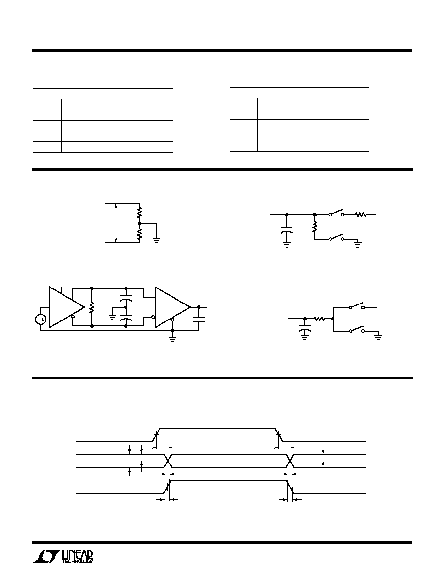
Figure 2. Receiver Timing Test Load
Figure 1. Driver DC Test Load
Figure 5. Driver Propagation Delays
SWITCHI G TI E WAVEFOR S
U
W
W
Figure 4. Driver Timing Test Load
Figure 3. Driver/Receiver Timing Test Circuit
V
OD
A
B
R
R
V
OC
LTC1480 · F01
RECEIVER
OUTPUT
C
RL
1k
S1
S2
TEST POINT
V
CC
1k
LTC1480 · F02
3V
DE
A
B
DI
R
DIFF
C
L1
C
L2
RO
15pF
A
B
RE
LTC1480 · F03
LTC1480
RECEIVER
LTC1480
DRIVER
OUTPUT
UNDER TEST
C
L
S1
S2
V
CC
500
LTC1480 · F04
DI
3V
1.5V
t
PLH
t
r
t
SKEW
1/2 V
O
V
O
f = 1MHz, t
r
10ns, t
f
10ns
90%
10%
0V
B
A
V
O
V
O
0V
90%
1.5V
t
PHL
t
SKEW
1/2 V
O
10%
t
f
V
DIFF
= V(A) V(B)
LTC1480 · F05
TEST CIRCUITS