
1
LTC1483
Ultra-Low Power RS485 Low EMI
Transceiver with Shutdown
S
FEATURE
D
U
ESCRIPTIO
The LTC
Æ
1483 is an ultra-low power differential line trans-
ceiver designed for data transmission standard RS485
applications with extended common-mode range (≠ 7V to
12V). It will also meet the requirements of RS422. The
LTC1483 features output drivers with controlled slew rate,
decreasing the EMI radiated from the RS485 lines, and
improving signal fidelity with misterminated lines. The
CMOS design offers significant power savings over its
bipolar counterparts without sacrificing ruggedness against
overload or ESD damage. Typical quiescent current is only
80
µ
A while operating and less than 1
µ
A in shutdown.
The driver and receiver feature three-state outputs, with
the driver outputs maintaining high impedance over the
entire common-mode range. Excessive power dissipation
caused by bus contention or faults is prevented by a
thermal shutdown circuit which forces the driver outputs
into a high impedance state. The receiver has a fail-safe
feature which guarantees a high output state when the
inputs are left open. I/O pins are protected against multiple
ESD strikes of over
±
10kV.
The LTC1483 is fully specified over the commercial and
extended industrial temperature range and is available in
8-pin DIP and SO packages.
s
Low Power: I
CC
= 120
µ
A Max with Driver Disabled
s
I
CC
= 500
µ
A Max with Driver Enabled, No Load
s
1
µ
A Quiescent Current in Shutdown Mode
s
Controlled Slew Rate Driver for Reduced EMI
s
Single 5V Supply
s
Drivers/Receivers Have
±
10kV ESD Protection
s
≠ 7V to 12V Common-Mode Range Permits
±
7V
Ground Difference Between Devices on the Data Line
s
Thermal Shutdown Protection
s
Power Up/Down Glitch-Free Driver Outputs Permit
Live Insertion or Removal of Transceiver
s
Driver Maintains High Impedance in Three-State
or with the Power Off
s
Up to 32 Transceivers on the Bus
s
Pin Compatible with the LTC485
s
Battery-Powered RS485/RS422 Applications
s
Low Power RS485/RS422 Transceiver
s
Level Translator
U
S
A
O
PPLICATI
U
A
O
PPLICATI
TYPICAL
V
CC1
GND1
R
RO1
RE1
DE1
DI1
D
V
CC2
GND2
R
RO2
RE2
DE2
DI2
D
R
TERM
R
TERM
LTC1483 ∑ TA01
RO
A ≠ B
DI
1483 TA02
, LTC and LT are registered trademarks of Linear Technology Corporation.
2
LTC1483
SYMBOL
PARAMETER
CONDITIONS
MIN
TYP
MAX
UNITS
V
OD1
Differential Driver Output Voltage (Unloaded)
I
O
= 0
q
5
V
V
OD2
Differential Driver Output Voltage (with Load)
R = 50
(RS422)
q
2
V
R = 27
(RS485), Figure 1
q
1.5
5
V
V
OD
Change in Magnitude of Driver Differential Output
R = 27
or R = 50
, Figure 1
q
0.2
V
Voltage for Complementary Output States
V
OC
Driver Common-Mode Output Voltage
R = 27
or R = 50
, Figure 1
q
3
V
V
OC
Change in Magnitude of Driver Common-Mode
R = 27
or R = 50
, Figure 1
q
0.2
V
Output Voltage for Complementary Output States
V
IH
Input High Voltage
DE, DI, RE
q
2
V
V
IL
Input Low Voltage
DE, DI, RE
q
0.8
V
I
IN1
Input Current
DE, DI, RE
q
±
2
µ
A
I
IN2
Input Current (A, B)
DE = 0, V
CC
= 0V or 5.25V, V
IN
= 12V
q
1.0
mA
DE = 0, V
CC
= 0V or 5.25V, V
IN
= ≠ 7V
q
≠ 0.8
mA
V
TH
Differential Input Threshold Voltage for Receiver
≠ 7V
V
CM
12V
q
≠ 0.2
0.2
V
V
TH
Receiver Input Hysteresis
V
CM
= 0V
q
45
mV
V
OH
Receiver Output High Voltage
I
O
= ≠ 4mA, V
ID
= 200mV
q
3.5
V
V
OL
Receiver Output Low Voltage
I
O
= 4mA, V
ID
= ≠ 200mV
q
0.4
V
I
OZR
Three-State (High Impedance) Output
V
CC
= Max, 0.4V
V
O
2.4V
q
±
1
µ
A
Current at Receiver
R
IN
Receiver Input Resistance
≠ 7V
V
CM
12V
q
12
25
k
I
CC
Supply Current
No Load, Output Enabled
q
300
500
µ
A
No Load, Output Disabled
q
80
120
µ
A
I
SHDN
Supply Current in Shutdown Mode
DE = 0, RE = V
CC
1
10
µ
A
I
OSD1
Driver Short-Circuit Current, V
OUT
= HIGH
≠ 7V
V
O
12V
q
35
250
mA
I
OSD2
Driver Short-Circuit Current, V
OUT
= LOW
≠ 7V
V
O
12V
q
35
250
mA
I
OSR
Receiver Short-Circuit Current
0V
V
O
V
CC
q
7
85
mA
A
U
G
W
A
W
U
W
A
R
BSOLUTE
XI
TI
S
W
U
U
PACKAGE/ORDER I FOR ATIO
ORDER PART
NUMBER
LTC1483CN8
LTC1483IN8
LTC1483CS8
LTC1483IS8
(Note 1)
Supply Voltage (V
CC
) .............................................. 12V
Control Input Voltage ..................... ≠ 0.5V to V
CC
+ 0.5V
Driver Input Voltage ....................... ≠ 0.5V to V
CC
+ 0.5V
Driver Output Voltage ...........................................
±
14V
Receiver Input Voltage ..........................................
±
14V
Receiver Output Voltage ................ ≠ 0.5V to V
CC
+ 0.5V
Operating Temperature Range
LTC1483C ........................................ 0
∞
C
T
A
70
∞
C
LTC1483I .................................... ≠ 40
∞
C
T
A
85
∞
C
Lead Temperature (Soldering, 10 sec) ................. 300
∞
C
T
JMAX
= 125
∞
C,
JA
= 130
∞
C/ W (N8)
T
JMAX
= 125
∞
C,
JA
= 150
∞
C/ W (S8)
S8 PART MARKING
1483
1483I
Consult factory for Military grade parts.
ELECTRICAL C
C
HARA TERISTICS
V
CC
= 5V, (Notes 2, 3) unless otherwise noted.
1
2
3
4
8
7
6
5
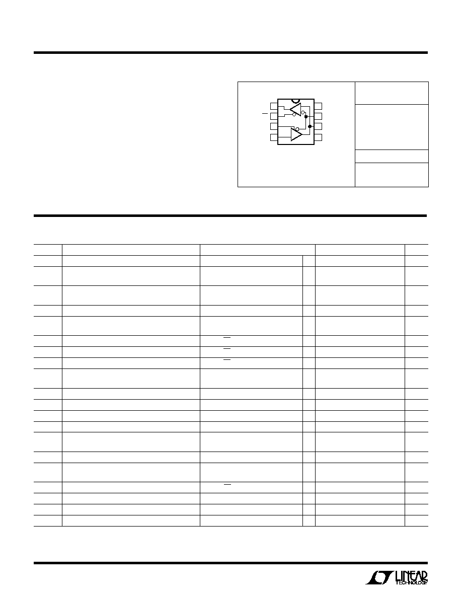
TOP VIEW
V
CC
B
A
GND
N8 PACKAGE
8-LEAD PDIP
S8 PACKAGE
8-LEAD PLASTIC SO
R
D
RO
RE
DE
DI

3
LTC1483
V
CC
= 5V, (Notes 2, 3) unless otherwise noted.
SWITCHI G CHARACTERISTICS
U
Note 2: All currents into device pins are positive; all currents out ot device
pins are negative. All voltages are referenced to device ground unless
otherwise specified.
Note 3: All typicals are given for V
CC
= 5V and T
A
= 25
∞
C.
The
q
denotes specifications which apply over the full operating
temperature range.
Note 1: Absolute maximum ratings are those beyond which the safety of
the device cannot be guaranteed.
Supply Current vs Temperature
Receiver
t
PLH
≠ t
PHL
vs
Temperature
TEMPERATURE (
∞
C)
≠50
14
12
10
8
6
4
2
0
25
75
1483 G02
≠25
0
50
100
125
t
PLH
≠ t
PHL
(ns)
Driver Differential Output Voltage
vs Output Current
OUTPUT VOLTAGE (V)
0
70
60
50
40
30
20
10
0
3
1483 G03
1
2
4
5
OUTPUT CURRENT (mA)
T
A
= 25
∞
C
TYPICAL PERFOR
M
A
N
CE CHARACTERISTICS
U
W
TEMPERATURE (
∞
C)
≠50
SUPPLY CURRENT (
µ
A)
50
350
300
250
200
150
100
50
0
1483 G01
0
≠25
25
75
125
175
150
100
DRIVER ENABLED
DRIVER DISABLED
THERMAL SHUTDOWN
WITH DRIVER ENABLED
LTC1483
SYMBOL
PARAMETER
CONDITIONS
MIN
TYP
MAX
UNITS
t
PLH
Driver Input to Output
R
DIFF
= 54
, C
L1
= C
L2
= 100pF,
q
150
1200
ns
t
PHL
Driver Input to Output
q
150
1200
ns
t
SKEW
Driver Output to Output
q
100
600
ns
t
r
, t
f
Driver Rise or Fall Time
q
150
1200
ns
t
ZH
Driver Enable to Output High
C
L
= 100pF (Figures 4, 6), S2 Closed
q
100
1500
ns
t
ZL
Driver Enable to Output Low
C
L
= 100pF (Figures 4, 6), S1 Closed
q
100
1500
ns
t
LZ
Driver Disable Time from Low
C
L
= 15pF (Figures 4, 6), S1 Closed
q
150
1500
ns
t
HZ
Driver Disable Time from High
C
L
= 15pF (Figures 4, 6), S2 Closed
q
150
1500
ns
t
PLH
Receiver Input to Output
R
DIFF
= 54
, C
L1
= C
L2
= 100pF,
q
30
140
200
ns
t
PHL
Receiver Input to Output
q
30
140
200
ns
t
SKD
t
PLH
≠ t
PHL
Differential Receiver Skew
q
13
ns
t
ZL
Receiver Enable to Output Low
C
RL
= 15pF (Figures 2, 8), S1 Closed
q
20
50
ns
t
ZH
Receiver Enable to Output High
C
RL
= 15pF (Figures 2, 8), S2 Closed
q
20
50
ns
t
LZ
Receiver Disable from Low
C
RL
= 15pF (Figures 2, 8), S1 Closed
q
20
50
ns
t
HZ
Receiver Disable from High
C
RL
= 15pF (Figures 2, 8), S2 Closed
q
20
50
ns
f
MAX
Maximum Data Rate
q
250
kbits/s
t
SHDN
Time to Shutdown
DE = 0, RE =
q
50
200
600
ns
t
ZH(SHDN)
Driver Enable from Shutdown to Output High
C
L
= 100pF (Figures 4, 6), S2 Closed
q
2000
ns
t
ZL(SHDN)
Driver Enable from Shutdown to Output Low
C
L
= 100pF (Figures 4, 6), S1 Closed
q
2000
ns
t
ZH(SHDN)
Receiver Enable from Shutdown to Output High
C
L
= 15pF (Figures 2, 8), S2 Closed
q
3500
ns
t
ZL(SHDN)
Receiver Enable from Shutdown to Output Low
C
L
= 15pF (Figures 2, 8), S1 Closed
q
3500
ns
(Figures 3, 5)
(Figures 3, 7)

4
LTC1483
TYPICAL PERFOR
M
A
N
CE CHARACTERISTICS
U
W
Driver Differential Output Voltage
vs Temperature
TEMPERATURE (
∞
C)
≠50
DIFFERENTIAL VOLTAGE (V)
2.5
2.4
2.3
2.2
2.1
2.0
1.9
1.8
1.7
1.6
1.5
0
50
75
1483 G04
≠25
25
100
125
R
L
= 54
Driver Output High Voltage
vs Output Current
OUTPUT VOLTAGE (V)
0
OUTPUT CURRENT (mA)
2
4
5
0
≠10
≠20
≠30
≠40
≠50
≠60
≠70
≠80
≠90
1483 G06
1
3
T
A
= 25
∞
C
PI
N
FU
N
CTIO
N
S
U
U
U
DI (Pin 4): Driver Input. If the driver outputs are enabled
(DE high) then a low on DI forces the outputs A low and B
high. A high on DI with the driver outputs enabled will force
A high and B low.
GND (Pin 5): Ground.
A (Pin 6): Driver Output/Receiver Input.
B (Pin 7): Driver Output/Receiver Input.
V
CC
(Pin 8): Positive Supply. 4.75V < V
CC
< 5.25V.
RO (Pin 1): Receiver Output. If the receiver output is
enabled (RE low), then if A > B by 200mV, RO will be high.
If A < B by 200mV, then RO will be low.
RE (Pin 2): Receiver Output Enable. A low enables the
receiver output, RO. A high input forces the receiver
output into a high impedance state.
DE (Pin 3): Driver Outputs Enable. A high on DE enables
the driver output. A, B and the chip will function as a line
driver. A low input will force the driver outputs into a high
impedance state and the chip will function as a line
receiver. If RE is high and DE is low, the part will enter a low
power (1
µ
A) shutdown state.
FU CTIO TABLES
U
U
LTC1483 Transmitting
INPUTS
OUTPUTS
RE
DE
DI
B
A
X
1
1
0
1
X
1
0
1
0
0
0
X
Z
Z
1
0
X
Z*
Z*
*Shutdown mode for LTC1483
LTC1483 Receiving
INPUTS
OUTPUTS
RE
DE
A ≠ B
RO
0
0
0.2V
1
0
0
≠ 0.2V
0
0
0
Inputs Open
1
1
0
X
Z*
*Shutdown mode for LTC1483
OUTPUT VOLTAGE
0
70
60
50
40
30
20
10
0
3
1483 G05
1
2
4
OUTPUT CURRENT (mA)
T
A
= 25
∞
C
Driver Output Low Voltage
vs Output Current
5
LTC1483
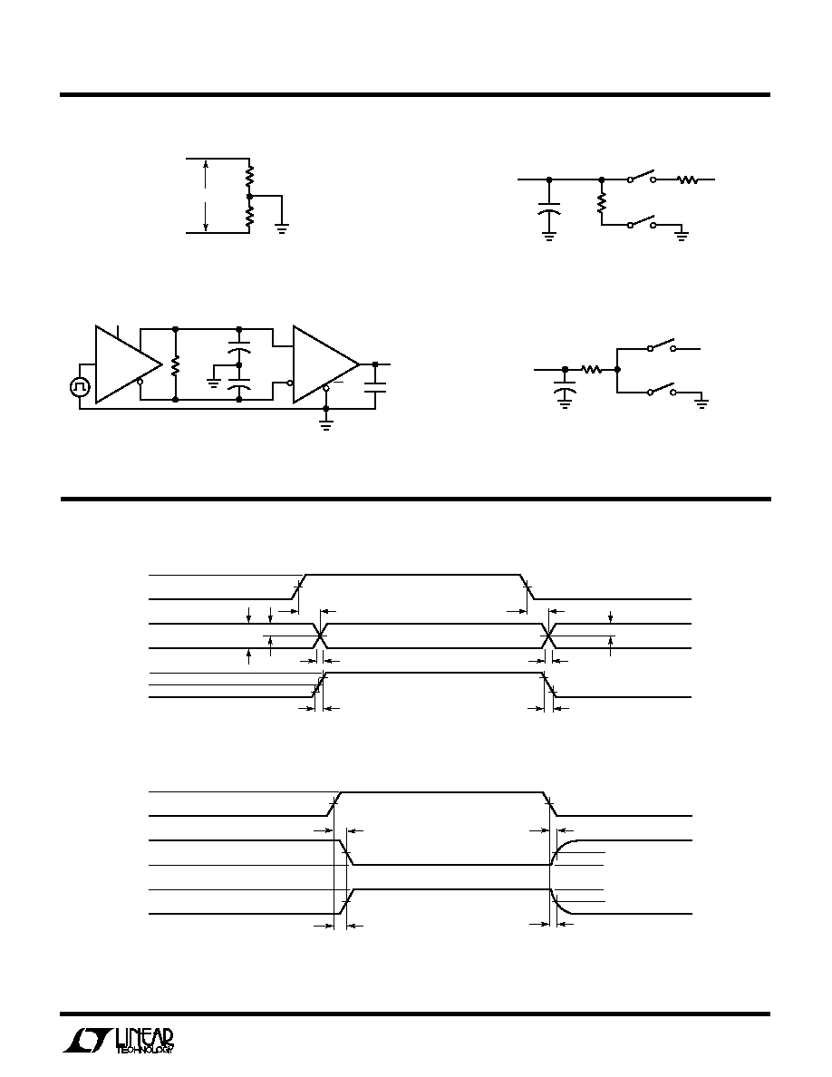
TEST CIRCUITS
SWITCHI G TI E WAVEFOR S
U
W
W
3V
DE
A
B
DI
R
DIFF
C
L1
C
L2
RO
15pF
A
B
RE
LTC1483 ∑ F03
Figure 3. Driver/ Receiver Timing Test Circuit
Figure 4. Driver Timing Test Load
OUTPUT
UNDER TEST
C
L
S1
S2
V
CC
500
LTC1483 ∑ F04
V
OD
A
B
R
R
V
OC
LTC1483 ∑ F01
RECEIVER
OUTPUT
C
RL
1k
S1
S2
TEST POINT
V
CC
1k
LTC1483 ∑ F02
Figure 1. Driver DC Test Load
Figure 2. Receiver Timing Test Load
Figure 6. Driver Enable and Disable Times
1.5V
2.3V
2.3V
t
ZH(SHDN)
,
t
ZH
t
ZL(SHDN)
,
t
ZL
1.5V
t
LZ
0.5V
0.5V
t
HZ
OUTPUT NORMALLY LOW
OUTPUT NORMALLY HIGH
3V
0V
DE
5V
V
OL
V
OH
0V
A, B
A, B
LTC1483 ∑ F06
t
r
10ns, t
f
10ns
Figure 5. Driver Propagation Delays
DI
3V
1.5V
t
PLH
t
r
t
SKEW
1/2 V
O
V
O
t
r
10ns, t
f
10ns
90%
10%
0V
B
A
V
O
≠V
O
0V
90%
1.5V
t
PHL
t
SKEW
1/2 V
O
10%
t
f
V
DIFF
= V(A) ≠ V(B)
LTC1483 ∑ F05

6
LTC1483
SWITCHI G TI E WAVEFOR S
U
W
W
1.5V
t
PHL
RO
≠V
OD2
A ≠ B
0V
0V
1.5V
t
PLH
OUTPUT
INPUT
V
OD2
V
OL
V
OH
LTC1483 ∑ F07
t
r
10ns, t
f
10ns
Figure 7. Receiver Propagation Delays
1.5V
t
ZL(SHDN)
, t
ZL
t
ZH(SHDN)
, t
ZH
1.5V
1.5V
1.5V
t
LZ
0.5V
0.5V
t
HZ
OUTPUT NORMALLY LOW
OUTPUT NORMALLY HIGH
3V
0V
RE
5V
0V
RO
RO
LTC1483 ∑ F08
t
r
10ns, t
f
10ns
Figure 8. Receiver Enable and Disable Times
APPLICATIO S I FOR ATIO
U
U
W
U
Basic Theory of Operation
Traditionally RS485 transceivers have been designed us-
ing bipolar technology because the common-mode range
of the device must extend beyond the supplies and the
device must be immune to ESD damage and latch-up.
Unfortunately, most bipolar devices draw a large amount
of supply current, which is unacceptable for the numerous
applications that require low power consumption. The
LTC1483 is a CMOS RS485/RS422 transceiver which
features ultra-low power consumption without sacrificing
ESD and latch-up immunity.
The LTC1483 uses a proprietary driver output stage,
which allows a common-mode range that extends beyond
the power supplies while virtually eliminating latch-up and
providing excellent ESD protection. Figure 9 shows the
LTC1483 output stage while Figure 10 shows a conven-
tional CMOS output stage.
When the conventional CMOS output stage of Figure 10
enters a high impedance state, both the P-channel (P1)
and the N-channel (N1) are turned off. If the output is then
driven above V
CC
or below ground, the P+/N -well diode
(D1) or the N+/P-substrate diode (D2) respectively will
turn on and clamp the output to the supply. Thus, the
output stage is no longer in a high impedance state and is
not able to meet the RS485 common-mode range require-
ment. In addition, the large amount of current flowing
through either diode will induce the well-known CMOS
latch-up condition, which could destroy the device.
LOGIC
V
CC
SD3
P1
D1
OUTPUT
SD4
D2
N1
LTC1483 ∑ F09
Figure 9. LTC1483 Output Stage
LOGIC
V
CC
P1
D1
OUTPUT
D2
N1
LTC1483 ∑ F10
Figure 10. Conventional
CMOS Output Stage
7
LTC1483
APPLICATIO S I FOR ATIO
U
U
W
U
The LTC1483 output stage of Figure 9 eliminates these
problems by adding two Schottky diodes, SD3 and SD4.
The Schottky diodes are fabricated by a proprietary modi-
fication to the standard N-well CMOS process. When the
output stage is operating normally, the Schottky diodes
are forward biased and have a small voltage drop across
them. When the output is in the high impedance state and
is driven above V
CC
or below ground, the parasitic diode
D1 or D2 still turns on, but SD3 or SD4 will reverse bias and
prevent current from flowing into the N-well or the sub-
strate. Thus the high impedance state is maintained even
with the output voltage beyond the supplies. With no
minority carrier current flowing into the N-well or sub-
strate, latch-up is virtually eliminated under power-up or
power-down conditions.
The LTC1483 output stage will maintain a high impedance
state until the breakdown of the N-channel or P-channel is
reached when going positive or negative respectively. The
output will be clamped to either V
CC
or ground by a Zener
voltage plus a Schottky diode drop, but this voltage is well
beyond the RS485 operating range. An ESD cell protects
output against multiple
±
10kV human body model ESD
strikes. Because the ESD injected current in the N-well or
substrate consists of majority carriers, latch-up is pre-
vented by careful layout techniques.
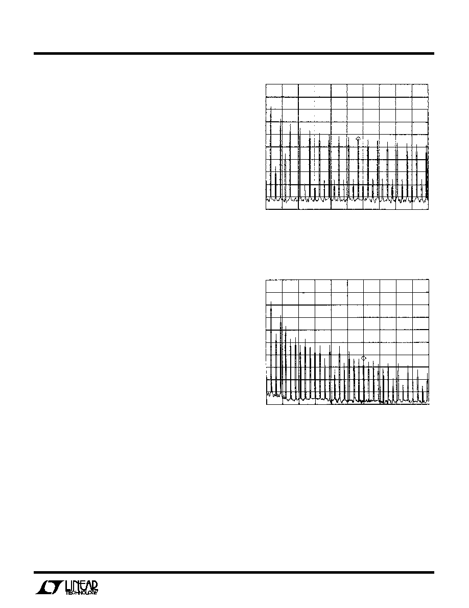
Slew Rate
The LTC1483 is designed for systems that are sensitive to
electromagnetic radiation. The part features a slew rate
limited driver that reduces high frequency electromag-
netic emissions, while improving signal fidelity by reduc-
ing reflections due to misterminated cables. Figures 11
and 12 show the spectrum of the signal at the driver output
for a standard slew rate RS485 driver and the slew rate
limited LTC1483. The LTC1483 shows significant reduc-
tion of the high frequency harmonics. Because the driver
is slew rate limited, the maximum operating frequency is
limited to 250kbits/s.
Low Power Operation
The LTC1483 is designed to operate with a quiescent
current of 120
µ
A max. With the driver in three-state I
CC
will
Information furnished by Linear Technology Corporation is believed to be accurate and reliable.
However, no responsibility is assumed for its use. Linear Technology Corporation makes no represen-
tation that the interconnection of circuits as described herein will not infringe on existing patent rights.
0
5
4
3
FREQUENCY (MHz)
2
1
20
10
0
≠10
≠20
≠30
≠40
≠50
≠60
≠70
≠80
LOG MAGNITUDE (dBV
RMS
)
0
5
4
3
FREQUENCY (MHz)
2
1
20
10
0
≠10
≠20
≠30
≠40
≠50
≠60
≠70
≠80
LOG MAGNITUDE (dBV
RMS
)
drop to this 120
µ
A level. With the driver enabled there will
be additional current drawn by the internal 12k resistor.
Under normal operating conditions this additional current
is overshadowed by the current drawn by the external bus
impedance.
Figure 12. Slew Rate Limited LTC1483 Driver Output
Spectrum Transmitting at 150kHz
Figure 11. Typical RS485 Driver Output Spectrum
Transmitting at 150kHz
8
LTC1483
©
LINEAR TECHNOLOGY CORPORATION 1994
LT/GP 1094 10K ∑ PRINTED IN THE USA
Linear Technology Corporation
1630 McCarthy Blvd., Milpitas, CA 95035-7487
(408) 432-1900
q
FAX
: (408) 434-0507
q
TELEX
: 499-3977
APPLICATIO S I FOR ATIO
U
U
W
U
Shutdown Mode
Both the receiver output (RO) and the driver outputs (A, B)
can be placed in three-state mode by bringing RE high and
DE low respectively. In addition, the LTC1483 will enter
shutdown mode when RE is high and DE is low.
In shutdown the LTC1483 typically draws only 1
µ
A of
supply current. In order to guarantee that the part goes
into shutdown, RE must be high and DE must be low for
at least 600ns simultaneously. If this time duration is less
than 50ns the part will not enter shutdown mode. Toggling
either RE or DE will wake the LTC1483 back up within
3.5
µ
s.
If the slow slew rate driver was active immediately prior to
shutdown, the supply current will not drop to 1
µ
A until the
driver outputs have reached a steady state; this can take as
long as 2.6
µ
s under worst case conditions. If the driver
was disabled prior to shutdown the supply current will
drop to 1
µ
A immediately.
RELATED PARTS
PART NUMBER
DESCRIPTION
COMMENTS
LTC485
5V Low Power RS485 Interface Transceiver
Low Power
LTC1480
3.3V Ultra-Low Power RS485 Transceiver
World's First 3V Powered 485 Transceiver with Low Power Consumption
LTC1481
5V Ultra-Low Power RS485 Transceiver with Shutdown
Lowest Power
LTC1485
5V Differential Bus Transceiver
Highest Speed
LTC1487
5V Ultra-Low Power RS485 with Low EMI Shutdown
High Input Impendance/Low EMI/Lowest Power
and High Input Impendance
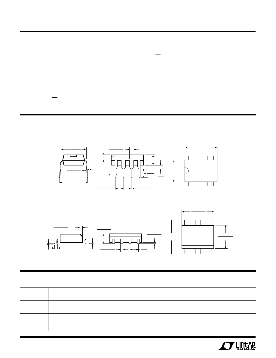
Dimension in inches (millimeters) unless otherwise noted.
PACKAGE DESCRIPTIO
N
U
N Package
8-Lead Plastic DIP
N8 0695
0.005
(0.127)
MIN
0.100
±
0.010
(2.540
±
0.254)
0.065
(1.651)
TYP
0.045 ≠ 0.065
(1.143 ≠ 1.651)
0.130
±
0.005
(3.302
±
0.127)
0.015
(0.380)
MIN
0.018
±
0.003
(0.457
±
0.076)
0.125
(3.175)
MIN
1
2
3
4
8
7
6
5
0.255
±
0.015*
(6.477
±
0.381)
0.400*
(10.160)
MAX
0.009 ≠ 0.015
(0.229 ≠ 0.381)
0.300 ≠ 0.325
(7.620 ≠ 8.255)
0.325
+0.025
≠0.015
+0.635
≠0.381
8.255
(
)
*THESE DIMENSIONS DO NOT INCLUDE MOLD FLASH OR PROTRUSIONS.
MOLD FLASH OR PROTRUSIONS SHALL NOT EXCEED 0.010 INCH (0.254mm)
1
2
3
4
0.150 ≠ 0.157**
(3.810 ≠ 3.988)
8
7
6
5
0.189 ≠ 0.197*
(4.801 ≠ 5.004)
0.228 ≠ 0.244
(5.791 ≠ 6.197)
0.016 ≠ 0.050
0.406 ≠ 1.270
0.010 ≠ 0.020
(0.254 ≠ 0.508)
◊
45
∞
0
∞
≠ 8
∞
TYP
0.008 ≠ 0.010
(0.203 ≠ 0.254)
SO8 0695
0.053 ≠ 0.069
(1.346 ≠ 1.752)
0.014 ≠ 0.019
(0.355 ≠ 0.483)
0.004 ≠ 0.010
(0.101 ≠ 0.254)
0.050
(1.270)
BSC
DIMENSION DOES NOT INCLUDE MOLD FLASH. MOLD FLASH
SHALL NOT EXCEED 0.006" (0.152mm) PER SIDE
DIMENSION DOES NOT INCLUDE INTERLEAD FLASH. INTERLEAD
FLASH SHALL NOT EXCEED 0.010" (0.254mm) PER SIDE
*
**
S Package
8-Lead Plastic SOIC