Äîêóìåíòàöèÿ è îïèñàíèÿ www.docs.chipfind.ru
1
LTC1484
Low Power
RS485 Transceiver
with Receiver Fail-Safe
s
No Damage or Latchup to
±
15kV ESD (Human
Body Model), IEC-1000-4-2 Level 4 Contact (
±
8kV)
and Level 3 (
±
8kV) Air Gap Specifications
s
Guaranteed High Receiver Output State for Floating,
Shorted or Terminated Inputs with No Signal
Present
s
Drives Low Cost Residential Telephone Wires
s
Low Power: I
CC
= 700
µ
A Max with Driver Disabled
s
I
CC
= 900
µ
A Max for Driver Enable with No Load
s
20
µ
A Max Quiescent Current in Shutdown Mode
s
Single 5V Supply
s
7V to 12V Common Mode Range Permits
±
7V
Ground Difference Between Devices on the Data Line
s
Power Up/Down Glitch-Free Driver Outputs
s
Up to 32 Transceivers on the Bus
s
Pin Compatible with the LTC485
s
Available in 8-Lead MSOP, PDIP and SO Packages
The LTC
®
1484 is a low power RS485 compatible trans-
ceiver. In receiver mode, it offers a fail-safe feature which
guarantees a high receiver output state when the inputs
are left open, shorted together or terminated with no
signal present. No external components are required to
ensure the high receiver output state.
Both driver and receiver feature three-state outputs with
separate receiver and driver control pins. The driver
outputs maintain high impedance over the entire com-
mon mode range when three-stated. Excessive power
dissipation caused by bus contention or faults is pre-
vented by a thermal shutdown circuit that forces the
driver outputs into a high impedance state.
Enhanced ESD protection allows the LTC1484 to with-
stand
±
15kV (human body model), IEC-1000-4-2 level 4
(
±
8kV) contact and level 3 (
±
8kV) air discharge ESD
without latchup or damage.
The LTC1484 is fully specified over the commercial and
industrial temperature ranges and is available in 8-lead
MSOP, PDIP and SO packages.
s
Battery-Powered RS485/RS422 Applications
s
Low Power RS485/RS422 Transceiver
s
Level Translator
, LTC and LT are registered trademarks of Linear Technology Corporation.
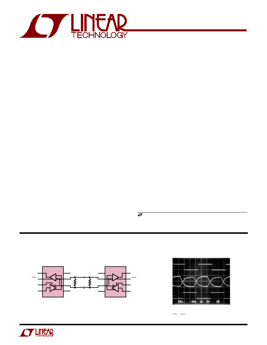
RO1
RE1
DE1
DI1
R
V
CC1
LTC1484
GND1
B1
A1
B2
A2
120
120
D
V
CC2
GND2
1484 TA01
R
D
RO2
RE2
DE2
DI2
LTC1484
RS485 Interface
APPLICATIO S
U
FEATURES
TYPICAL APPLICATIO
U
DESCRIPTIO
U
Driving a 2000 Foot STP Cable
Dl1
DE1 = V
CC
1484 TA01a
Dl2 = 0
DE2 = 0
RE1 = RE2 = 0
Dl1
B2
A2
RO2
2
LTC1484
ABSOLUTE
M
AXI
M
U
M
RATINGS
W
W
W
U
(Note 1)
Supply Voltage (V
CC
)............................................... 6.5V
Control Input Voltages ................. 0.3V to (V
CC
+ 0.3V)
Driver Input Voltage ..................... 0.3V to (V
CC
+ 0.3V)
Driver Output Voltages ................................. 7V to 10V
Receiver Input Voltages (Driver Disabled) .. 12V to 14V
Receiver Output Voltage ............... 0.3V to (V
CC
+ 0.3V)
Junction Temperature .......................................... 125
°
C
Operating Temperature Range
LTC1484C ......................................... 0
°
C
T
A
70
°
C
LTC1484I ...................................... 40
°
C
T
A
85
°
C
Storage Temperature Range ................. 65
°
C to 150
°
C
Lead Temperature (Soldering, 10 sec).................. 300
°
C
The
q
denotes the specifications which apply over the full operating
temperature range, otherwise specifications are at T
A
= 25
°
C. V
CC
= 5V
±
5% (Notes 2 and 3) unless otherwise noted.
SYMBOL
PARAMETER
CONDITIONS
MIN
TYP
MAX
UNITS
V
OD1
Differential Driver Output Voltage (Unloaded)
I
OUT
= 0
q
V
CC
V
V
OD2
Differential Driver Output Voltage (with Load)
R = 50
(RS422)
q
2
V
R = 27
(RS485) Figure 1
q
1.5
5
V
R = 22
, Figure 1
q
1.5
5
V
V
OD3
Differential Driver Output Voltage
V
TST
= 7V to 12V, Figure 2
q
1.5
5
V
(with Common Mode)
V
OD
Change in Magnitude of Driver Differential
R = 22
, 27
or R = 50
, Figure 1
q
0.2
V
Output Voltage for Complementary Output States
V
TST
= 7V to 12V, Figure 2
V
OC
Driver Common Mode Output Voltage
R = 22
, 27
or R = 50
, Figure 1
q
3
V
|V
OC
|
Change in Magnitude of Driver Common Mode
R = 22
, 27
or R = 50
, Figure 1
q
0.2
V
Output Voltage for Complementary Output States
V
IH
Input High Voltage
DE, DI, RE
q
2.0
V
V
IL
Input Low Voltage
DE, DI, RE
q
0.8
V
I
IN1
Input Current
DE, DI, RE
q
±
2
µ
A
I
IN2
Input Current (A, B)
DE = 0, V
CC
= 0 or 5V, V
IN
= 12V
q
1.0
mA
DE = 0, V
CC
= 0 or 5V, V
IN
= 7V
q
0.8
mA
V
TH
Differential Input Threshold Voltage for Receiver
7V
V
CM
12V, DE = 0
q
0.20
0.015
V
ELECTRICAL CHARACTERISTICS
PACKAGE/ORDER I
N
FOR
M
ATIO
N
W
U
U
ORDER PART
NUMBER
ORDER PART
NUMBER
LTC1484CMS8
LTC1484CN8
LTC1484CS8
LTC1484IN8
LTC1484IS8
S8 PART MARKING
1484
1484I
MS8 PART MARKING
LTDX
T
JMAX
= 125
°
C,
JA
= 200
°
C/ W
T
JMAX
= 125
°
C,
JA
= 130
°
C/ W (N8)
T
JMAX
= 125
°
C,
JA
= 135
°
C/ W (S8)
Consult factory for Military grade parts.
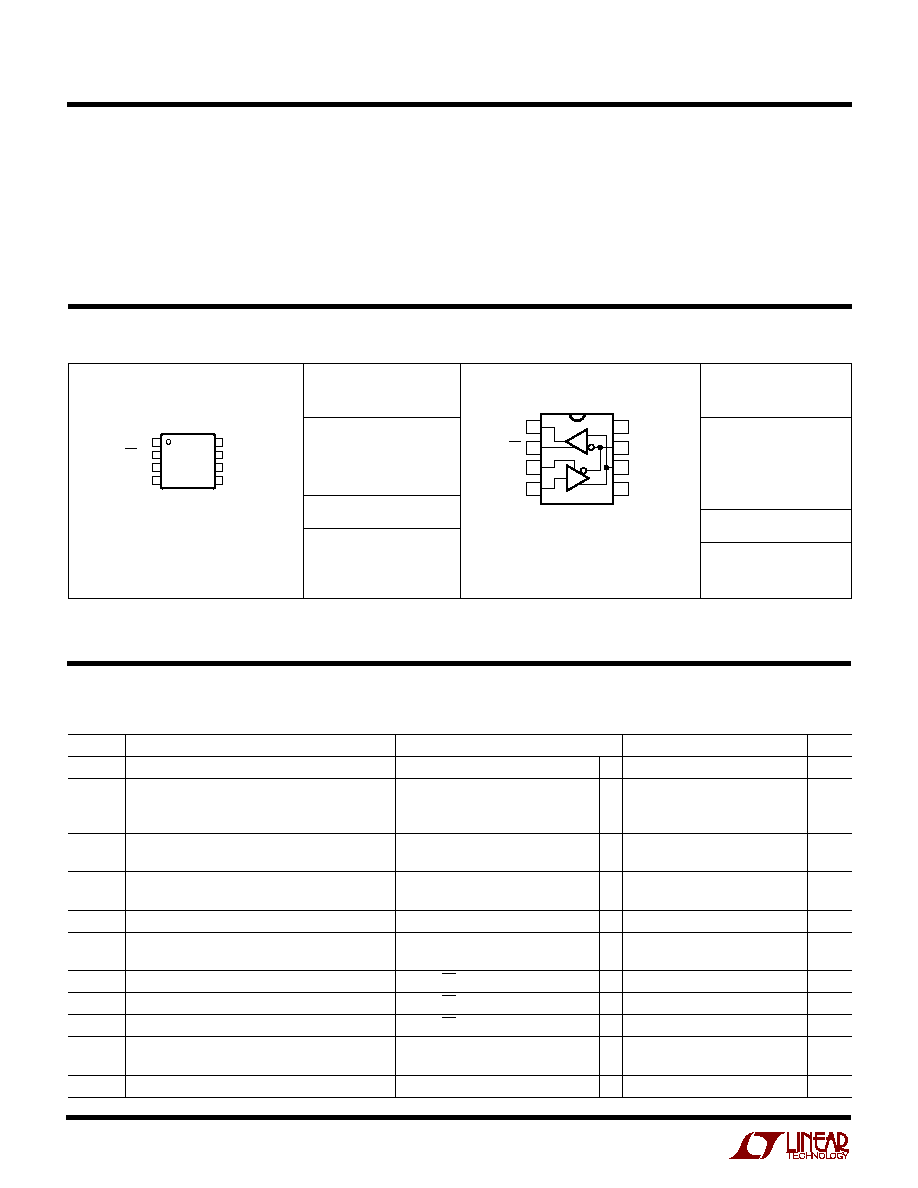
1
2
3
4
RO
RE
DE
DI
8
7
6
5
V
CC
B
A
GND
TOP VIEW
MS8 PACKAGE
8-LEAD PLASTIC MSOP
1
2
3
4
8
7
6
5
TOP VIEW
RO
RE
DE
DI
V
CC
B
A
GND
N8 PACKAGE
8-LEAD PDIP
S8 PACKAGE
8-LEAD PLASTIC SO
R
D
3
LTC1484
SYMBOL
PARAMETER
CONDITIONS
MIN
TYP
MAX
UNITS
V
TH
Receiver Input Hysteresis
V
CM
= 0V, DE = 0
q
±
30
mV
V
OH
Receiver Output High Voltage
I
OUT
= 4mA, (V
A
V
B
) = 200mV
q
3.5
V
V
OL
Receiver Output Low Voltage
I
OUT
= 4mA, (V
A
V
B
) = 200mV
q
0.4
V
I
OZR
Three-State (High Impedance) Output Current
V
CC
= Max, 0.4V
V
OUT
2.4V,
q
±
1
µ
A
at Receiver
DE = 0
R
IN
Receiver Input Resistance
7V
V
CM
12V
q
12
22
k
I
CC
Supply Current
No Load, Output Enabled (DE = V
CC
)
q
600
900
µ
A
No Load, Output Disabled (DE = 0)
q
400
700
µ
A
I
SHDN
Supply Current in Shutdown Mode
DE = 0, RE = V
CC
, DI = 0
q
1
20
µ
A
I
OSD1
Driver Short-Circuit Current, V
OUT
= High (Note 4)
7V
V
OUT
10V
35
250
mA
I
OSD2
Driver Short-Circuit Current, V
OUT
= Low (Note 4)
7V
V
OUT
10V
35
250
mA
I
OSR
Receiver Short-Circuit Current
0V
V
OUT
V
CC
q
7
85
mA
The
q
denotes the specifications which apply over the full operating
temperature range, otherwise specifications are at T
A
= 25
°
C. V
CC
= 5V
±
5% (Notes 2 and 3) unless otherwise noted.
ELECTRICAL CHARACTERISTICS
SWITCHI
N
G CHARACTERISTICS
U
SYMBOL
PARAMETER
CONDITIONS
MIN
TYP
MAX
UNITS
t
PLH
Driver Input to Output
R
DIFF
= 54
, C
L1
= C
L2
= 100pF
q
10
28.5
60
ns
(Figures 4, 6)
t
PHL
Driver Input to Output
R
DIFF
= 54
, C
L1
= C
L2
= 100pF
q
10
31
60
ns
(Figures 4, 6)
t
SKEW
Driver Output to Output
R
DIFF
= 54
, C
L1
= C
L2
= 100pF
q
2.5
10
ns
(Figures 4, 6)
t
r
, t
f
Driver Rise or Fall Time
R
DIFF
= 54
, C
L1
= C
L2
= 100pF
q
3
15
40
ns
(Figures 4, 6)
t
ZH
Driver Enable to Output High
C
L
= 100pF (Figures 5, 7) S2 Closed
q
40
70
ns
t
ZL
Driver Enable to Output Low
C
L
= 100pF (Figures 5, 7) S1 Closed
q
40
100
ns
t
LZ
Driver Disable Time from Low
C
L
= 15pF (Figures 5, 7) S1 Closed
q
40
70
ns
t
HZ
Driver Disable Time from High
C
L
= 15pF (Figures 5, 7) S2 Closed
q
40
70
ns
t
PLH
Receiver Input to Output
R
DIFF
= 54
, C
L1
= C
L2
= 100pF,
q
30
160
200
ns
(Figures 4, 8)
t
PHL
Receiver Input to Output
R
DIFF
= 54
, C
L1
= C
L2
= 100pF,
q
30
140
200
ns
(Figures 4, 8)
t
SKD
|t
PLH
t
PHL
| Differential Receiver Skew
R
DIFF
= 54
, C
L1
= C
L2
= 100pF,
20
ns
(Figures 4, 8)
t
ZL
Receiver Enable to Output Low
C
RL
= 15pF (Figures 3, 9) S1 Closed
q
20
50
ns
t
ZH
Receiver Enable to Output High
C
RL
= 15pF (Figures 3, 9) S2 Closed
q
20
50
ns
t
LZ
Receiver Disable from Low
C
RL
= 15pF (Figures 3, 9) S1 Closed
q
20
50
ns
t
HZ
Receiver Disable from High
C
RL
= 15pF (Figures 3, 9) S2 Closed
q
20
50
ns
t
DZR
Driver Enable to Receiver Valid
R
DIFF
= 54
, C
L1
= C
L2
= 100pF
q
1600
3000
ns
(Figures 4, 10)
f
MAX
Maximum Data Rate (Note 5)
q
4
5
Mbps
t
SHDN
Time to Shutdown (Note 6)
DE = 0, RE
q
50
300
600
ns
The
q
denotes the specifications which apply over the full operating
temperature range, otherwise specifications are at T
A
= 25
°
C.
4
LTC1484
SYMBOL
PARAMETER
CONDITIONS
MIN
TYP
MAX
UNITS
t
ZH(SHDN)
Driver Enable from Shutdown to Output High
C
L
= 100pF (Figures 5, 7) S2 Closed,
q
40
100
ns
DI = DE
t
ZL(SHDN)
Driver Enable from Shutdown to Output Low
C
L
= 100pF (Figures 5, 7) S1 Closed,
q
40
100
ns
DI = 0
t
ZH(SHDN)
Receiver Enable from Shutdown to Output High
C
L
= 15pF (Figures 3, 9) S2 Closed,
q
10
µ
s
DE = 0
t
ZL(SHDN)
Receiver Enable from Shutdown to Output Low
C
L
= 15pF (Figures 3, 9) S1 Closed,
q
10
µ
s
DE = 0
Note 1: Absolute Maximum Ratings are those values beyond which the life of
a device may be impaired.
Note 2: All typicals are given for V
CC
= 5V and T
A
= 25
°
C.
Note 3: All currents into device pins are positive; all currents out of device
pins are negative. All voltages are referenced to device ground unless
otherwise specified.
Note 4: For higher ambient temperatures, the part may enter thermal
shutdown during short-circuit conditions.
Note 5: Guaranteed by design.
Note 6: Time for I
CC
to drop to I
CC
/2 when the receiver is disabled.
SWITCHI
N
G CHARACTERISTICS
U
The
q
denotes the specifications which apply over the full operating
temperature range, otherwise specifications are at T
A
= 25
°
C. V
CC
= 5V
±
5% (Notes 2 and 3) unless otherwise noted.
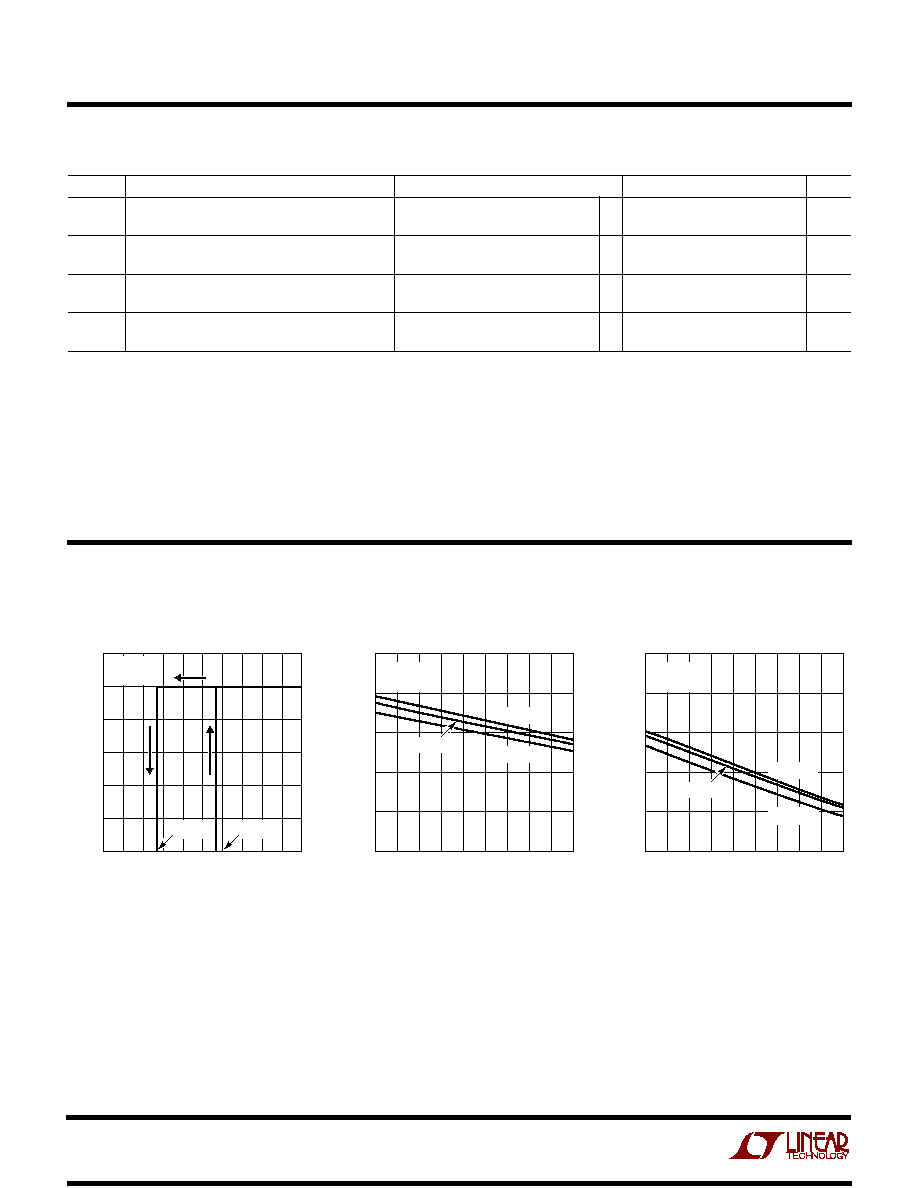
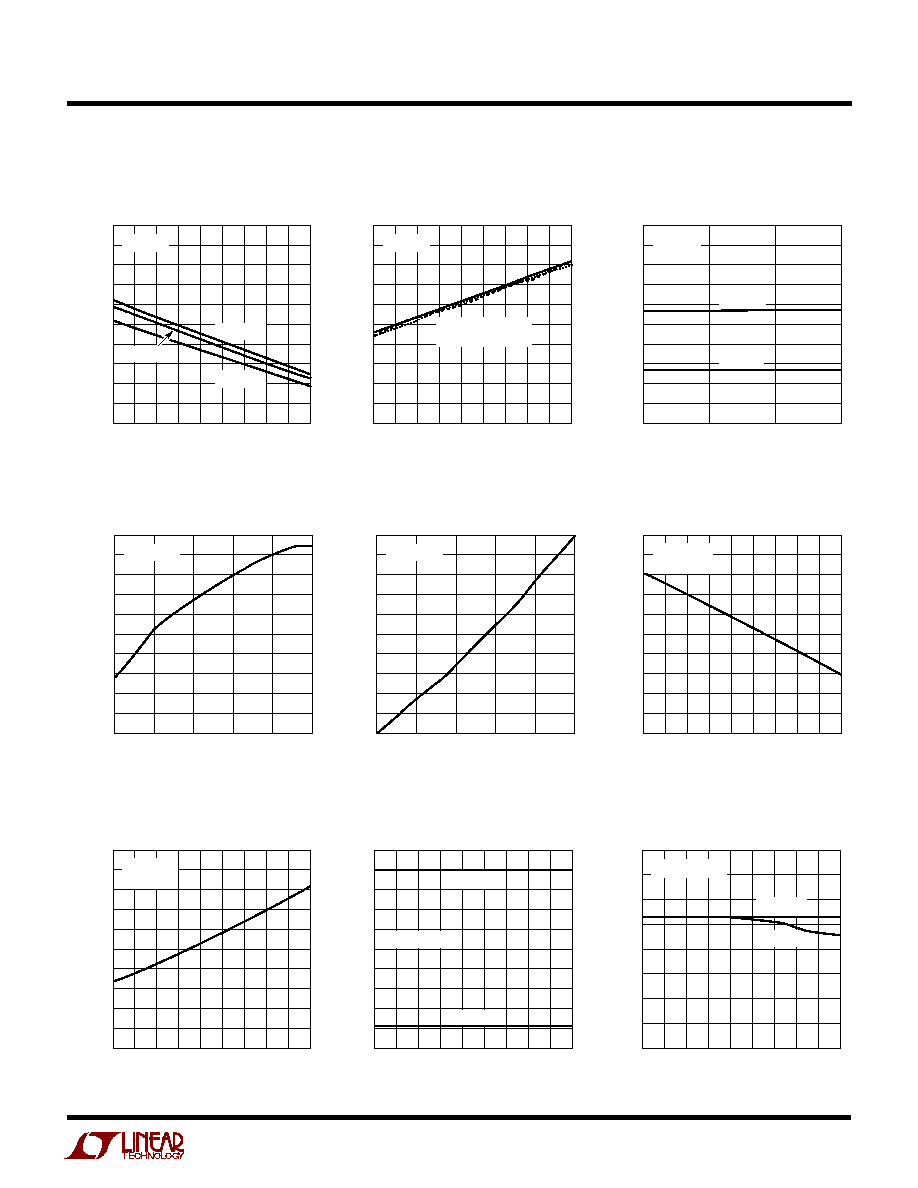
TYPICAL PERFOR A CE CHARACTERISTICS
U
W
INPUT VOLTAGE (V)
0.2
0.16
0.12
0.08
0.04
0
RECEIVER OUTPUT VOLTAGE (V)
1484 G01
6
5
4
3
2
1
0
T
A
= 25
°
C
V
CC
= 5V
V
TH(HIGH)
V
TH(LOW)
TEMPERATURE (
°
C)
55 35 15
5
25
45
65
85 105 125
RECEIVER INPUT THRESHOLD VOLTAGE (V)
1484 G02
0
0.05
0.10
0.15
0.20
0.25
V
CC
= 5V
V
TH(HIGH)
V
CM
= 7V
V
CM
= 12V
V
CM
= 0V
TEMPERATURE (
°
C)
55 35 15
5
25
45
65
85 105 125
RECEIVER INPUT THRESHOLD VOLTAGE (V)
1484 G03
0
0.05
0.10
0.15
0.20
0.25
V
CC
= 5V
V
TH(LOW)
V
CM
= 7V
V
CM
= 12V
V
CM
= 0V
Receiver Output Voltage vs Input
Voltage
Receiver Input Threshold Voltage
(Output High) vs Temperature
Receiver Input Threshold Voltage
(Output Low) vs Temperature
5
LTC1484
TYPICAL PERFOR A CE CHARACTERISTICS
U
W
TEMPERATURE (
°
C)
55 35 15
5
25
45
65
85 105 125
RECEIVER INPUT OFFSET VOLTAGE (mV)
1484 G04
0
20
40
60
80
100
120
140
160
180
200
V
CC
= 5V
V
CM
= 7V
V
CM
= 12V
V
CM
= 0V
TEMPERATURE (
°
C)
55 35 15
5
25
45
65
85 105 125
RECEIVER HYSTERESIS (mV)
1484 G05
100
90
80
70
60
50
40
30
20
10
0
V
CC
= 5V
V
TH(HIGH)
V
TH(LOW)
V
CM
= 7V TO 12V
SUPPLY VOLTAGE (V)
4.5
4.75
5
5.25
RECEIVER INPUT THRESHOLD VOLTAGE (V)
1484 G06
0
0.02
0.04
0.06
0.08
0.10
0.12
0.14
0.16
0.18
0.20
T
A
= 25
°
C
V
CM
= 0V
V
TH(HIGH)
V
TH(LOW)
Receiver Input Offset Voltage vs
Temperature
Receiver Hysteresis vs
Temperature
Receiver Input Threshold Voltage
vs Supply Voltage
Receiver Output High Voltage vs
Output Current
Receiver Output Low Voltage vs
Output Current
Receiver Output High Voltage vs
Temperature
OUTPUT CURRENT (mA)
25
20
15
10
5
0
RECEIVER OUTPUT HIGH VOLTAGE (V)
1484 G07
5.0
4.5
4.0
3.5
3.0
2.5
2.0
1.5
1.0
0.5
0
V
CC
= 4.75V
OUTPUT CURRENT (mA)
0
5
10
15
20
25
RECEIVER OUTPUT LOW VOLTAGE (V)
1484 G08
1.0
0.9
0.8
0.7
0.6
0.5
0.4
0.3
0.2
0.1
0
V
CC
= 4.75V
TEMPERATURE (
°
C)
55 35 15
5
25
45
65
85 105 125
RECEIVER OUTPUT HIGH VOLTAGE (V)
1484 G09
4.5
4.4
4.3
4.2
4.1
4.0
3.9
3.8
3.7
3.6
3.5
V
CC
= 4.75V
I
OUT
= 8mA
Receiver Output Low Voltage vs
Temperature
Input Current (A, B) vs
Temperature
Receiver Input Resistance vs
Temperature
TEMPERATURE (
°
C)
55 35 15
5
25
45
65
85 105 125
RECEIVER OUTPUT LOW VOLTAGE (V)
1484 G10
0.50
0.45
0.40
0.35
0.30
0.25
0.20
0.15
0.10
0.05
0
V
CC
= 4.75V
I
OUT
= 8mA
TEMPERATURE (
°
C)
55 35 15
5
25
45
65
85 105 125
INPUT CURRENT (
µ
A)
1484 G11
600
500
400
300
200
100
0
100
200
300
400
V
CC
= 0V OR 5V
V
CM
= 12V
V
CM
= 7V
TEMPERATURE (
°
C)
55 35 15
5
25
45
65
85 105 125
RECEIVER INPUT RESISTANCE (k
)
1484 G12
26.0
25.5
25.0
24.5
24.0
23.5
23.0
22.5
22.0
V
CC
= 0V OR 5V
V
CM
= 12V
V
CM
= 7V