Äîêóìåíòàöèÿ è îïèñàíèÿ www.docs.chipfind.ru
1
LTC1485
Differential Bus Transceiver
D
U
ESCRIPTIO
S
FEATURE
, LTC and LT are registered trademarks of Linear Technology Corporation.
U
A
O
PPLICATI
TYPICAL
DI
RO
4
3
6
7
2
DE
120
120
DRIVER
RECEIVER
DE
3
4
RO
DI
2
1
6
7
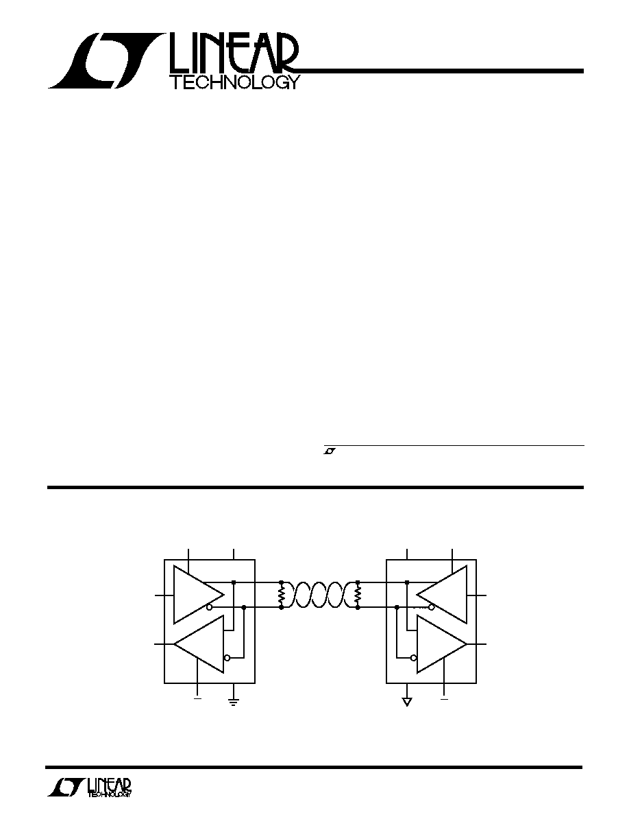
4000 FT 24 GAUGE TWISTED PAIR
1485 TA01
LTC1485
LTC1485
RECEIVER
DRIVER
RE
RE
8
5V
8
5V
5
5
1
The LTC
®
1485 is a low power differential bus/line trans-
ceiver designed for multipoint data transmission standard
RS485 applications with extended common-mode range
(12V to 7V). It also meets the requirements of RS422.
The CMOS with Schottky design offers significant power
savings over its bipolar counterpart without sacrificing
ruggedness against overload or ESD damage.
The driver and receiver feature three-state outputs, with
the driver outputs maintaining high impedance over the
entire common-mode range. Excessive power dissipation
caused by bus contention or faults is prevented by a
thermal shutdown circuit which forces the driver outputs
into a high impedance state. I/O pins are protected against
multiple ESD strikes of over
±
10kV.
The receiver has a fail-safe feature which guarantees a
high output state when the inputs are left open.
Both AC and DC specifications are guaranteed from 40
°
C
to 85
°
C and 4.75V to 5.25V supply voltage range.
s
Low Power RS485/RS422 Transceiver
s
Level Translator
U
S
A
O
PPLICATI
s
ESD Protection over
±
10kV
s
Low Power: I
CC
= 1.8mA Typ
s
28ns Typical Driver Propagation Delays with
4ns Skew
s
Designed for RS485 or RS422 Applications
s
Single 5V Supply
s
7V to 12V Bus Common-Mode Range Permits
±
7V
Ground Difference Between Devices on the Bus
s
Thermal Shutdown Protection
s
Power-Up/Down Glitch-Free Driver Outputs
s
Driver Maintains High Impedance in Three-State or
with the Power Off
s
Combined Impedance of a Driver Output and
Receiver Allows up to 32 Transceivers on the Bus
s
60mV Typical Input Hysteresis
s
Pin Compatible with the SN75176A, DS75176A, and
SN75LBC176
2
LTC1485
A
U
G
W
A
W
U
W
A
R
BSOLUTE
XI
TI
S
W
U
U
PACKAGE/ORDER I FOR ATIO
(Note 1)
Supply Voltage (V
CC
) .............................................. 12V
Control Input Voltages ................... 0.5V to V
CC
+ 0.5V
Control Input Currents ........................ 50mA to 50mA
Driver Input Voltages ..................... 0.5V to V
CC
+ 0.5V
Driver Input Currents .......................... 25mA to 25mA
Driver Output Voltages .........................................
±
14V
Receiver Input Voltages ........................................
±
14V
Receiver Output Voltages .............. 0.5V to V
CC
+ 0.5V
Operating Temperature Range
LTC1485C ............................................... 0
°
C to 70
°
C
LTC1485I .......................................... 40
°
C to 85
°
C
Storage Temperature Range ................ 65
°
C to 150
°
C
Lead Temperature (Soldering, 10 sec.) ................ 300
°
C
SYMBOL
PARAMETER
CONDITIONS
MIN
TYP
MAX
UNITS
V
OD1
Differential Driver Output Voltage (Unloaded)
I
O
= 0
q
5
V
V
OD2
Differential Driver Output Voltage (With Load)
R = 50
, (RS422)
q
2
V
R = 27
, (RS485) (Figure 1)
q
1.5
5
V
V
OD
Change in Magnitude of Driver Differential
R = 27
or R = 50
(Figure 1)
q
0.2
V
Output Voltage for Complementary Output States
V
OC
Driver Common-Mode Output Voltage
R = 27
or R = 50
(Figure 1)
q
3
V
| V
OC
|
Change in Magnitude of Driver Common-Mode
R = 27
or R = 50
(Figure 1)
q
0.2
V
Output Voltage for Complementary Output States
V
INH
Input High Voltage
DI, DE, RE
q
2.0
V
V
INL
Input Low Voltage
DI, DE, RE
q
0.8
V
I
IN1
Input Current
DI, DE, RE
q
±
2
µ
A
I
IN2
Input Current (A, B)
V
CC
= 0V or 5.25V, V
IN
= 12V
q
1.0
mA
V
CC
= 0V or 5.25V, V
IN
= 7V
q
0.8
mA
V
TH
Differential Input Threshold Voltage for Receiver
7V
V
CM
12V
q
0.2
0.2
V
V
TH
Receiver Input Hysteresis
V
CM
= 0V
q
60
mV
V
OH
Receiver Output High Voltage
I
O
= 4mA, V
ID
= 0.2V
q
3.5
V
V
OL
Receiver Output Low Voltage
I
O
= 4mA, V
ID
= 0.2V
q
0.4
V
I
OZR
Three-State Output Current at Receiver
V
CC
= Max 0.4V
V
O
2.4V
q
±
1
µ
A
I
CC
Supply Current
No Load; DI = GND or V
CC
Outputs Enabled
q
1.8
2.3
mA
Outputs Disabled
q
1.7
2.3
mA
R
IN
Receiver Input Resistance
7V
V
CM
12V
q
12
k
I
OSD1
Driver Short-Circuit Current, V
OUT
= High
V
O
= 7V
q
250
mA
I
OSD2
Driver Short-Circuit Current, V
OUT
= Low
V
O
= 10 V
q
250
mA
I
OSR
Receiver Short-Circuit Current
0V
V
O
V
CC
q
7
85
mA
V
CC
= 5V (Notes 2, 3), unless otherwise noted.
ELECTRICAL C
C
HARA TERISTICS
C
D
1
2
3
4
5
6
7
8
TOP VIEW
RO
B
V
CC
N8 PACKAGE
8-LEAD PLASTIC DIP
D
R
A
GND
DE
DI
S8 PACKAGE
8-LEAD PLASTIC SOIC
RE
T
JMAX
= 125
°
C,
JA
= 100
°
C/ W (N)
T
JMAX
= 150
°
C,
JA
= 150
°
C/ W (S)
Consult factory for Military grade parts.
ORDER PART
NUMBER
S8 PART MARKING
LTC1485CN8
LTC1485IN8
LTC1485CS8
LTC1485IS8
1485
1485I
3
LTC1485
SYMBOL
PARAMETER
CONDITIONS
MIN
TYP
MAX
UNITS
t
PLH
Driver Input to Output
R
DIFF
= 54
, C
L1
= C
L2
= 100pF
q
10
30
50
ns
(Figures 2, 5)
t
PHL
Driver Input to Output
R
DIFF
= 54
, C
L1
= C
L2
= 100pF
q
10
30
50
ns
(Figures 2, 5)
t
SKEW
Driver Output to Output
R
DIFF
= 54
, C
L1
= C
L2
= 100pF
q
4
10
ns
(Figures 2, 5)
t
r
, t
f
Driver Rise or Fall Time
R
DIFF
= 54
, C
L1
= C
L2
= 100pF
q
5
15
25
ns
(Figures 2, 5)
t
ZH
Driver Enable to Output High
C
L
= 100pF (Figures 4, 6) S2 Closed
q
40
70
ns
t
ZL
Driver Enable to Output Low
C
L
= 100pF (Figures 4, 6) S1 Closed
q
40
70
ns
t
LZ
Driver Disable Time from Low
C
L
= 15pF (Figures 4, 6) S1 Closed
q
40
70
ns
t
HZ
Driver Disable Time from High
C
L
= 15pF (Figures 4, 6) S2 Closed
q
40
70
ns
t
PLH
Receiver Input to Output
R
DIFF
= 54
, C
L1
= C
L2
= 100pF (Figures 2, 7)
q
15
25
50
ns
t
PHL
Receiver Input to Output
R
DIFF
= 54
, C
L1
= C
L2
= 100pF (Figures 2, 7)
q
20
30
55
ns
t
SKEW
| t
PLH
t
PHL
|
R
DIFF
= 54
, C
L1
= C
L2
= 100pF (Figures 2, 7)
q
5
15
ns
Differential Receiver Skew
t
ZL
Receiver Enable to Output Low
C
L
= 15pF (Figures 3, 8) S1 Closed
q
30
45
ns
t
ZH
Receiver Enable to Output High
C
L
= 15pF (Figures 3, 8) S2 Closed
q
30
45
ns
t
LZ
Receiver Disable from Low
C
L
= 15pF (Figures 3, 8) S1 Closed
q
30
45
ns
t
HZ
Receiver Disable from High
C
L
= 15pF (Figures 3, 8) S2 Closed
q
30
45
ns
S
U
G C
C
HARA TERISTICS
WITCHI
V
CC
= 5V (Notes 2, 3), unless otherwise noted.
The
q
denotes specifications which apply over the operating temperature
range.
Note 1: Absolute Maximum Ratings are those values beyond which the
safety of the device cannot be guaranteed.
Note 2: All currents into device pins are positive. All currents out of device
pins are negative. All voltages are referenced to device ground unless
otherwise specified.
Note 3: All typicals are given for V
CC
= 5V and T
A
= 25
°
C.
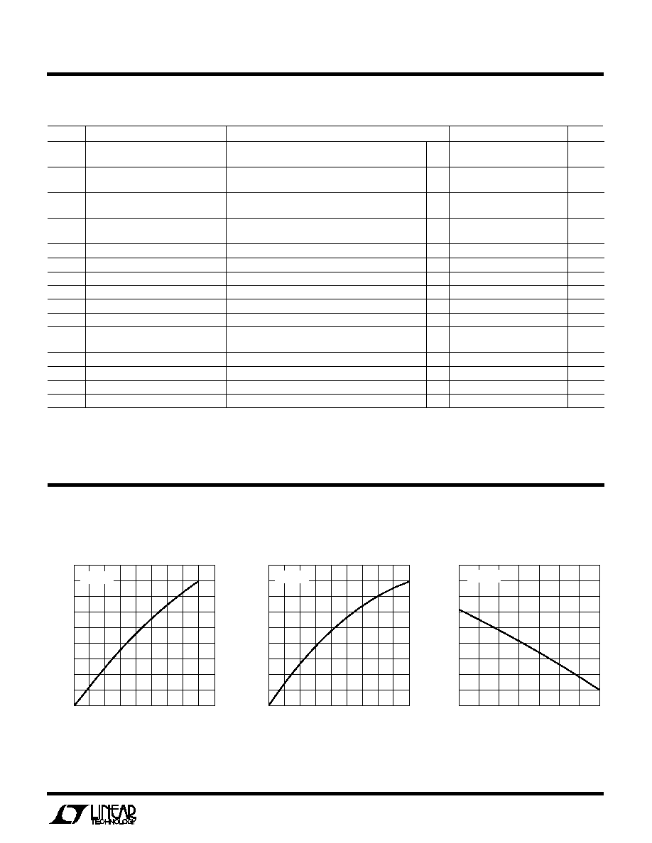
C
C
HARA TERISTICS
U
W
A
TYPICAL PERFOR
CE
Receiver Output High Voltage vs
Temperature
Receiver Output Low Voltage vs
Output Current
Receiver Output High Voltage vs
Output Current
OUTPUT VOLTAGE (V)
0
0
OUTPUT CURRENT (mA)
16
1.0
1485 G01
8
0.5
1.5
24
32
2.0
4
12
20
28
36
T
A
= 25
°
C
OUTPUT VOLTAGE (V)
5
0
OUTPUT CURRENT (mA)
8
1485 G02
4
4
3
12
16
2
2
6
10
14
18
T
A
= 25
°
C
TEMPERATURE (
°
C)
50
3.0
OUTPUT VOLTAGE (V)
3.8
50
1485 G03
3.4
25
125
4.2
4.6
0
25
75
100
4.8
4.4
4.0
3.6
3.2
I = 8mA
4
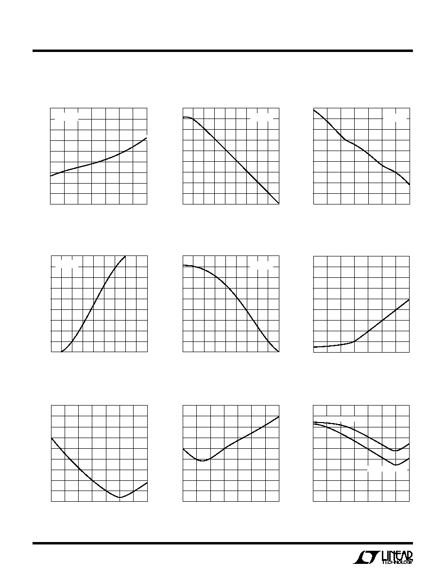
LTC1485
C
C
HARA TERISTICS
U
W
A
TYPICAL PERFOR
CE
Driver Differential Output Voltage
vs Temperature
TEMPERATURE (
°
C)
50
0
OUTPUT VOLTAGE (V)
0.1
0.3
0.4
0.5
50
0.9
1485 G04
0.2
25
125
0.6
0.7
0.8
0
25
75
100
I = 8mA
OUTPUT VOLTAGE (V)
0
0
OUTPUT CURRENT (mA)
32
2
1485 G05
16
1
3
48
64
4
T
A
= 25
°
C
TEMPERATURE (
°
C)
50
1.6
DIFFERENTIAL VOLTAGE (V)
2.0
50
1485 G06
1.8
25
125
2.2
2.4
0
25
75
100
R
L
=54
Driver Differential Output Voltage
vs Output Current
Receiver Output Low Voltage
vs Temperature
Driver Output High Voltage vs
Output Current
TTL Input Threshold vs
Temperature
Driver Output Low Voltage vs
Output Current
OUTPUT VOLTAGE (V)
0
0
OUTPUT CURRENT (mA)
40
2
1485 G07
20
1
3
60
80
4
T
A
= 25
°
C
OUTPUT VOLTAGE (V)
0
0
OUTPUT CURRENT (mA)
48
2
1485 G08
24
1
3
72
96
4
T
A
= 25
°
C
TEMPERATURE (°C)
50
1.55
INPUT THRESHOLD VOLTAGE (V)
1.59
50
1485 G09
1.57
25
125
1.61
1.63
0
25
75
100
Receiver | t
PLH
t
PHL
| vs
Temperature
Supply Current vs Temperature
Driver Skew vs Temperature
TEMPERATURE (°C)
50
1
TIME (ns)
3
50
1485 G10
2
25
125
4
5
0
25
75
100
TEMPERATURE (°C)
50
1
TIME (ns)
3
50
1485 G11
2
25
125
4
5
0
25
75
100
TEMPERATURE (°C)
50
1.4
SUPPLY CURRENT (mA)
1.6
50
1485 G12
1.5
25
125
1.7
1.8
0
25
75
100
DRIVER ENABLED
DRIVER DISABLED
5
LTC1485
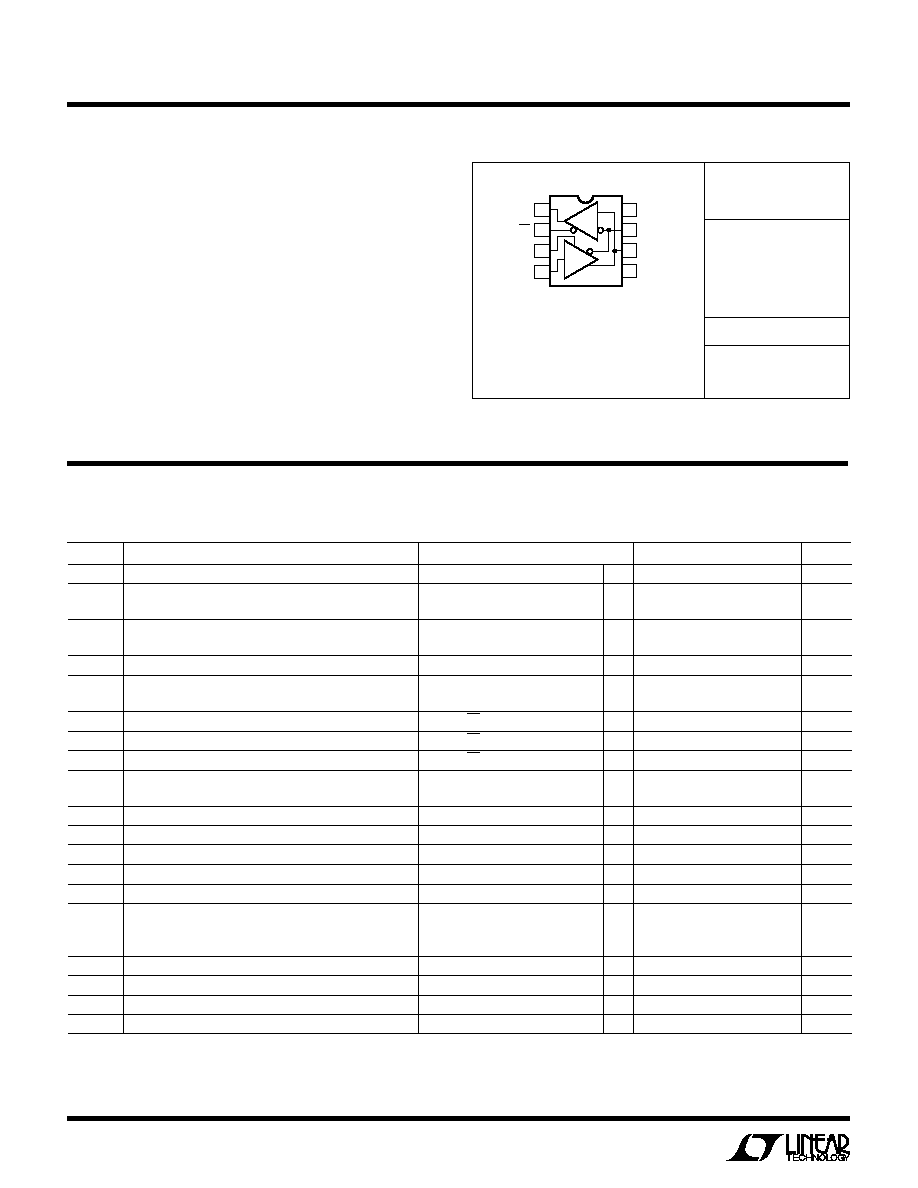
PI FU CTIO S
U
U
U
RO (Pin 1): Receiver Output. If the receiver output is
enabled (RE low), then if A > B by 200mV, RO will be high.
If A < B by 200mV, then RO will be low.
RE (Pin 2): Receiver Output Enable. A low enables the
receiver output, RO. A high input forces the receiver
output into a high impedance state.
DE (Pin 3): Driver Output Enable. A high on DE enables the
driver outputs, A and B. A low input will force the driver
outputs into a high impedance state.
DI (Pin 4): Driver Input. If the driver outputs are enabled
(DE high), then a low on DI forces the driver outputs A low
and B high. A high on DI will force A high and B low.
GND (Pin 5): Ground Connection.
A (Pin 6): Driver Output/Receiver Input.
B (Pin 7): Driver Output/Receiver Input.
V
CC
(Pin 8): Positive Supply. 4.75V
V
CC
5.25V.
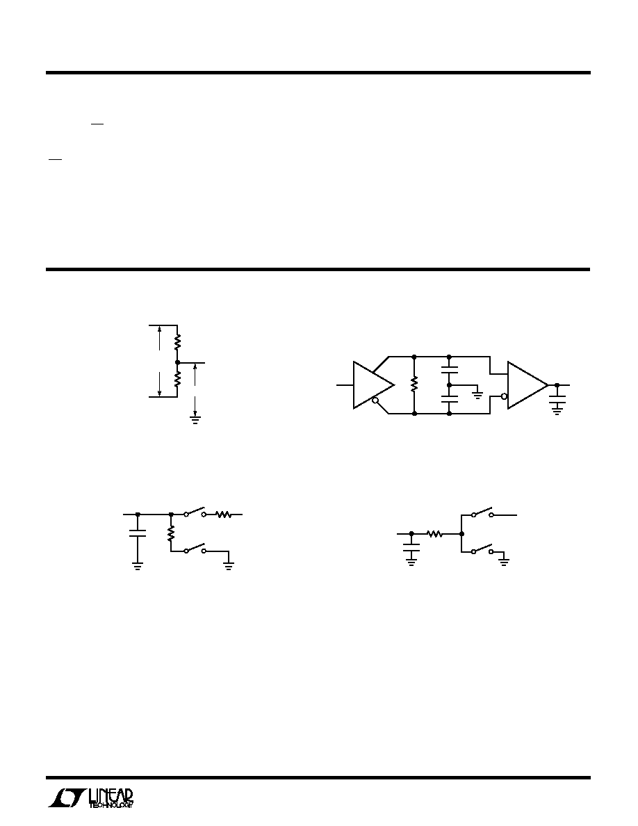
TEST CIRCUITS
Figure 3. Receiver Timing Test Load
1k
1485 F03
C
L
S1
S2
1k
V
CC
RECEIVER
OUTPUT
Figure 4. Driver Timing Test Load
1485 F04
C
L
S1
S2
500
V
CC
OUTPUT
UNDER TEST
V
OD2
A
B
R
R
V
OC
1485 F01
DI
R
DIFF
1485 F02
DRIVER
RECEIVER
C
L1
C
L2
RO
15pF
A
B
A
B
Figure 1. Driver DC Test Load
Figure 2. Driver/Receiver Timing Test Circuit