 | –≠–ª–µ–∫—Ç—Ä–æ–Ω–Ω—ã–π –∫–æ–º–ø–æ–Ω–µ–Ω—Ç: LTC1522 | –°–∫–∞—á–∞—Ç—å:  PDF PDF  ZIP ZIP |

1
LTC1522
Micropower, Regulated
5V Charge Pump
DC/DC Converter
The LTC
Æ
1522 is a micropower charge pump DC/DC
converter that produces a regulated 5V output from a 2.7V
to 5V input supply. Extremely low supply current (6
µ
A
typical with no load, < 1
µ
A in shutdown) and low external
parts count (one 0.22
µ
F flying capacitor and two 10
µ
F
capacitors at V
IN
and V
OUT
) make the LTC1522 ideally
suited for small, light load battery-powered applications.
Typical efficiency (V
IN
= 3V) exceeds 75% with load
currents between 50
µ
A and 20mA. Modulating the SHDN
pin keeps the typical efficiency above 75% with load
currents all the way down to 10
µ
A.
The LTC1522 has thermal shutdown and can survive a
continuous short from V
OUT
to GND. In shutdown the
load is disconnected from V
IN
. The part is available in
8-pin MSOP and SO packages. The LTC1522 is pin
compatible with the LTC1516 in applications where
V
IN
2.7V and I
OUT
20mA.
s
Ultralow Power: Typical Operating I
CC
= 6
µ
A
s
Short-Circuit/Thermal Protected
s
Regulated 5V
±
4% Output Voltage
s
2.7V to 5V Input Range
s
No Inductors
s
Very Low I
CC
in Shutdown: < 1
µ
A
s
Output Current: 10mA (V
IN
2.7V)
20mA (V
IN
3V)
s
Shutdown Disconnects Load from V
IN
s
Internal Oscillator: 700kHz
s
Compact Application Circuit (< 0.1 in
2
)
s
8-Pin MSOP and SO Packages
FEATURES
DESCRIPTIO
N
U
APPLICATIO
N
S
U
s
SIM Interface Supplies for GSM Cellular Telephones
s
Li-Ion Battery Backup Supplies
s
Local 3V to 5V Conversion
s
Smart Card Readers
s
PCMCIA Local 5V Supplies
TYPICAL APPLICATIO
N
U
1
2
3
4
8
7
6
5
NC
SHDN
GND
C
≠
NC
V
IN
V
OUT
C
+
LTC1522
ON/OFF
10
µ
F
10
µ
F
V
OUT
= 5V
±
4%
I
OUT
= 0mA TO 10mA, V
IN
2.7V
I
OUT
= 0mA TO 20mA, V
IN
3V
0.22
µ
F
V
IN
2.7V TO 5V
+
+
1522 TA01
Regulated 5V Output from a 2.7V to 5V Input
Efficiency vs Output Current
OUTPUT CURRENT (mA)
50
60
70
80
90
EFFICIENCY (%)
100
1522 TA02
0.01
0.1
1
10
SHDN = 0V
V
IN
= 3V
LOW I
Q
MODE
(SEE FIGURE 2)
, LTC and LT are registered trademarks of Linear Technology Corporation.

2
LTC1522
SYMBOL PARAMETER
CONDITIONS
MIN
TYP
MAX
UNITS
V
IN
Input Voltage
q
2.7
5
V
V
OUT
Output Voltage
2.7V
V
IN
5V, I
OUT
10mA
q
4.8
5.0
5.2
V
3V
V
IN
5V, I
OUT
20mA
q
4.8
5.0
5.2
V
I
CC
Operating Supply Current
2.7V
V
IN
5V, I
OUT
= 0mA, SHDN = 0V
q
6
15
µ
A
Shutdown Supply Current
2.7V
V
IN
3.6V, I
OUT
= 0mA, SHDN = V
IN
q
0.005
1
µ
A
3.6V <
V
IN
5V, I
OUT
= 0mA, SHDN = V
IN
q
2.5
µ
A
Output Ripple
V
IN
= 3V, I
OUT
= 10mA
70
mV
P-P
Efficiency
V
IN
= 3V, I
OUT
= 10mA
82
%
f
OSC
Switching Frequency
Oscillator Free Running
700
kHz
V
IH
SHDN Input Threshold
q
(0.7)(V
IN
)
V
V
IL
q
0.4
V
I
IH
SHDN Input Current
V
SHDN
= V
IN
q
≠ 1
1
µ
A
I
IL
V
SHDN
= 0V
q
≠ 1
1
µ
A
t
ON
V
OUT
Turn-On Time
V
IN
= 3V, I
OUT
= 0mA
1
ms
ABSOLUTE
M
AXI
M
U
M
RATINGS
W
W
W
U
(Note 1)
V
IN
to GND .................................................. ≠ 0.3V to 6V
V
OUT
to GND ............................................... ≠ 0.3V to 6V
SHDN to GND ............................................. ≠ 0.3V to 6V
V
OUT
Short-Circuit Duration ............................ Indefinite
Commercial Temperature Range ................ 0
∞
C to 70
∞
C
Extended Commercial Operating
Temperature Range (Note 2) ............. ≠ 40
∞
C to 85
∞
C
Storage Temperature Range ................ ≠ 65
∞
C to 150
∞
C
Lead Temperature (Soldering, 10 sec) ................. 300
∞
C
PACKAGE/ORDER I
N
FOR
M
ATIO
N
W
U
U
Consult factory for Industrial and Military grade parts.
S8 PART MARKING
ORDER PART
NUMBER
MS8 PART MARKING
ELECTRICAL CHARACTERISTICS
ORDER PART
NUMBER
The
q
denotes specifications which apply over the specified temperature
range.
Note 1: Absolute Maximum Ratings are those values beyond which the life
of the device may be impaired.
Note 2: C grade device specifications are guaranteed over the 0
∞
C to 70
∞
C
temperature range. In addition, C grade device specifications are assured
over the ≠ 40
∞
C to 85
∞
C temperature range by design or correlation, but
are not production tested.
V
IN
= 2.7V to 5V, C
FLY
= 0.22
µ
F, C
IN
= C
OUT
= 10
µ
F, T
MIN
to T
MAX
unless otherwise specified. (Note 2)
T
JMAX
= 125
∞
C,
JA
= 150
∞
C/ W
1
2
3
4
8
7
6
5
TOP VIEW
NC
SHDN
GND
C
≠
NC
V
IN
V
OUT
C
+
S8 PACKAGE
8-LEAD PLASTIC SO
LTCG
T
JMAX
= 125
∞
C,
JA
= 160
∞
C/ W
1
2
3
4
NC
V
IN
V
OUT
C
+
8
7
6
5
NC
SHDN
GND
C
≠
TOP VIEW
MS8 PACKAGE
8-LEAD PLASTIC MSOP
LTC1522CMS8
1522
LTC1522CS8

3
LTC1522
TYPICAL PERFOR
M
A
N
CE CHARACTERISTICS
U
W
INPUT VOLTAGE (V)
2.5
OUTPUT VOLTAGE (V)
5.05
5.10
5.15
4.5
1522 G01
5.00
4.95
4.90
3.0
3.5
4.0
5.0
I
OUT
= 10mA
C
OUT
= 10
µ
F
T
A
= 70
∞
C
T
A
= 25
∞
C
T
A
= 0
∞
C
INPUT VOLTAGE (V)
2.5
V
RIPPLE P-P
(mV) 150
200
250
4.5
1522 G03
100
50
0
3.0
3.5
4.0
5.0
I
OUT
= 10mA
C
FLY
= 0.1
µ
F
T
A
= 25
∞
C
C
OUT
= 6.8
µ
F
C
OUT
= 10
µ
F
C
OUT
= 22
µ
F
C
OUT
= 3.3
µ
F
INPUT VOLTAGE (V)
2.5
EFFICIENCY (%)
70
80
90
4.5
1522 G02
60
50
40
3.0
3.5
4.0
5.0
I
OUT
= 10mA
T
A
= 25
∞
C
Output Voltage vs Input Voltage
Efficiency vs Input Voltage
Output Ripple vs Input Voltage
No Load Input Current
vs Input Voltage
Typical Output Voltage
vs Output Current
OUTPUT CURRENT (mA)
0
OUTPUT VOLTAGE (V)
5.0
5.1
80
1522 G05
4.9
4.8
20
40
60
5.2
V
IN
= 3.3V
V
IN
= 3V
V
IN
= 2.7V
T
A
= 25
∞
C
C
FLY
= 0.1
µ
F
C
OUT
= 6.8
µ
F
Load Transient Response
I
OUT
0mA TO 10mA
10mA/DIV
V
OUT
AC COUPLED
50mV/DIV
V
IN
= 3V
500
µ
s/DIV
1522 G06
C
OUT
= 10
µ
F
PI
N
FU
N
CTIO
N
S
U
U
U
NC (Pin 1): No Connect.
V
IN
(Pin 2): Input Supply Voltage. Bypass V
IN
with a
3.3
µ
F low ESR capacitor.
V
OUT
(Pin 3): 5V Output Voltage (V
OUT
= 0V in Shutdown).
Bypass V
OUT
with a
3.3
µ
F low ESR capacitor.
C
+
(Pin 4): Flying Capacitor, Positive Terminal.
C
≠
(Pin 5): Flying Capacitor, Negative Terminal.
GND (Pin 6): Ground.
SHDN (Pin 7): Active High CMOS Logic-Level Shutdown
Input. Drive SHDN low to enable the DC/DC converter. Do
not float.
NC (Pin 8): No Connect.
INPUT VOLTAGE (V)
2.5
INPUT CURRENT (
µ
A)
7
8
9
4.5
1522 G04
6
5
4
3.0
3.5
4.0
5.0
I
OUT
= 0mA
T
A
= 70
∞
C
T
A
= 25
∞
C
T
A
= 0
∞
C
4
LTC1522
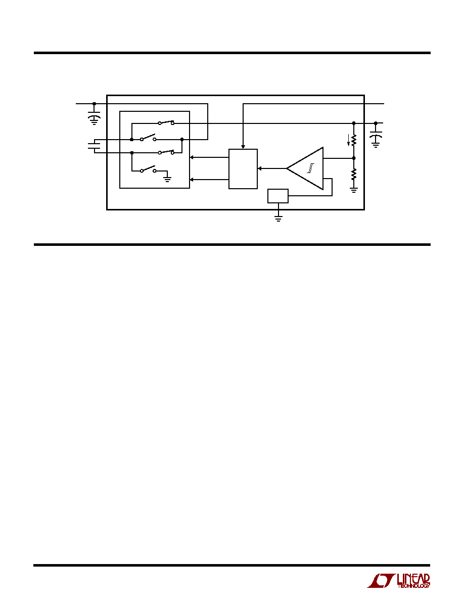
BLOCK DIAGRA
M
W
Operation
The LTC1522 uses a switched capacitor charge pump to
boost V
IN
to a regulated 5V
±
4% output voltage. Regula-
tion is achieved by sensing the output voltage through an
internal resistor divider and enabling the charge pump
when the output voltage droops below the lower trip point
of COMP1. When the charge pump is enabled, a 2-phase,
nonoverlapping clock controls the charge pump switches.
Clock 1 closes the S1 switches which enables the flying
capacitor to charge up to the V
IN
voltage. Clock 2 closes
the S2 switches that stack C
FLY
in series with V
IN
and
connect the top plate of C
FLY
to the output capacitor at
V
OUT
. This sequence of charging and discharging contin-
ues at a free-running frequency of 700kHz (typ) until the
output has risen to the upper trip point of COMP1 and the
charge pump is disabled. When the charge pump is
disabled, the LTC1522 draws only 4
µ
A (typ) from V
IN
which provides high efficiency at low load conditions.
In shutdown mode, all circuitry is turned off and the part
draws only leakage current from the V
IN
supply. V
OUT
is
also disconnected from V
IN
. The SHDN pin is a CMOS
input with a threshold of approximately V
IN
/2; however,
the SHDN pin can be driven by logic levels that exceed the
V
IN
voltage. The part enters shutdown mode when a logic
high is applied to the SHDN pin. The SHDN pin should not
be floated; it must be driven with a logic high or low.
Short-Circuit/Thermal Protection
During short-circuit conditions, the LTC1522 will draw
between 100mA and 200mA from V
IN
causing a rise in
the junction temperature. On-chip thermal shutdown
circuitry disables the charge pump once the junction
temperature exceeds
160
∞
C, and reenables the charge
pump once the junction temperature falls back to
145
∞
C.
The LTC1522 will cycle in and out of thermal shutdown
indefinitely without latchup or damage until the V
OUT
short is removed.
Capacitor Selection
For best performance, it is recommended that low ESR
(< 0.5
) capacitors be used for both C
IN
and C
OUT
to
reduce noise and ripple. The C
IN
and C
OUT
capacitors
should be either ceramic or tantalum and should be 3.3
µ
F
or greater (aluminum capacitors are not recommended
because of their high ESR). If the input source impedance
is very low, C
IN
may not be needed. Increasing the size of
C
OUT
to 10
µ
F or greater will reduce output voltage ripple.
APPLICATIO
N
S I
N
FOR
M
ATIO
N
W
U
U
U
V
REF
CLOCK 1
CLOCK 2
CONTROL
LOGIC
S2A
S2B
S1A
S1B
C
FLY
0.22
µ
F
C
IN
10
µ
F
C
+
C
≠
C
OUT
10
µ
F
1
µ
A
V
OUT
SHDN
LTC1522 BD
CHARGE PUMP SHOWN IN DISCHARGE CYCLE
V
IN
CHARGE PUMP
+
+
≠
+
COMP1

5
LTC1522
APPLICATIO
N
S I
N
FOR
M
ATIO
N
W
U
U
U
A ceramic capacitor is recommended for the flying capaci-
tor with a value in the range of 0.1
µ
F to 0.22
µ
F. Note that
a large value flying cap (> 0.22
µ
F) will increase output
ripple unless C
OUT
is also increased. For very low load
applications, C
FLY
may be reduced to 0.01
µ
F to 0.047
µ
F.
This will reduce output ripple at the expense of efficiency
and maximum output current.
Output Ripple
Normal LTC1522 operation produces voltage ripple on the
V
OUT
pin. Output voltage ripple is required for the LTC1522
to regulate. Low frequency ripple exists due to the hyster-
esis in the sense comparator and propagation delays in the
charge pump enable/disable circuits. High frequency ripple
is also present mainly due to ESR (Equivalent Series
Resistance) in the output capacitor. Typical output ripple
under maximum load is 50mV
P-P
with a low ESR 10
µ
F
output capacitor.
The magnitude of the ripple voltage depends on several
factors. High input voltages (V
IN
> 3.3V) increase the output
ripple since more charge is delivered to C
OUT
per clock
cycle. A large flying capacitor (> 0.22
µ
F) also increases
ripple for the same reason. Large output current load and/
or a small output capacitor (< 10
µ
F) results in higher ripple
due to higher output voltage dV/dt. High ESR capacitors
(ESR > 0.5
) on the output pin cause high frequency
voltage spikes on V
OUT
with every clock cycle.
There are several ways to reduce the output voltage ripple.
A larger C
OUT
capacitor (22
µ
F or greater) will reduce both
the low and high frequency ripple due to the lower C
OUT
charging and discharging dV/dt and the lower ESR typi-
cally found with higher value (larger case size) capacitors.
A low ESR ceramic output capacitor will minimize the high
frequency ripple, but will not reduce the low frequency
ripple unless a high capacitance value is chosen. A reason-
able compromise is to use a 10
µ
F to 22
µ
F tantalum
capacitor in parallel with a 1
µ
F to 3.3
µ
F ceramic capacitor
on V
OUT
to reduce both the low and high frequency ripple.
An RC filter may also be used to reduce high frequency
voltage spikes (see Figure 1).
V
OUT
5V
LTC1522
3
15
µ
F
TANTALUM
1
µ
F
CERAMIC
V
OUT
5V
V
OUT
+
LTC1522
3
1522 F01
3.9
10
µ
F
TANTALUM
10
µ
F
TANTALUM
V
OUT
+
+
Figure 1. Output Ripple Reduction Techniques
In low load or high V
IN
applications, smaller values for
C
FLY
may be used to reduce output ripple. A smaller flying
capacitor (0.01
µ
F to 0.047
µ
F) delivers less charge per
clock cycle to the output capacitor resulting in lower
output ripple. However, the smaller value flying caps also
reduce the maximum I
OUT
capability as well as efficiency.
Inrush Currents
During normal operation, V
IN
will experience current tran-
sients in the 50mA to 100mA range whenever the charge
pump is enabled. During start-up, these inrush currents
may approach 250mA. For this reason, it is important to
minimize the source resistance between the input supply
and the V
IN
pin. Too much source resistance may result in
regulation problems or even prevent start-up.
Ultralow Quiescent Current (I
Q
= 2.1
µ
A)
Regulated Supply
The LTC1522 contains an internal resistor divider (refer to
the Block Diagram) that draws only 1
µ
A (typ) from V
OUT
.
During no-load conditions, the internal load causes a
droop rate of only 100mV per second on V
OUT
with
C
OUT
= 10
µ
F. Applying a 2Hz to 100Hz, 95% to 98% duty
cycle signal to the SHDN pin ensures that the circuit of
Figure 2 comes out of shutdown frequently enough to
maintain regulation during no-load or low-load condi-
tions. Since the part spends nearly all of its time in
shutdown, the no-load quiescent current (see Figure 3a) is
approximately equal to (V
OUT
)(1
µ
A)/(V
IN
)(Efficiency).

6
LTC1522
APPLICATIO
N
S I
N
FOR
M
ATIO
N
W
U
U
U
Figure 2. Ultralow Quiescent Current (<2.1
µ
A) Regulated Supply
1
2
3
4
8
7
6
5
NC
SHDN
GND
C
≠
NC
V
IN
V
OUT
C
+
LTC1522
FROM MPU
10
µ
F
10
µ
F
V
OUT
5V
±
4%
SHDN PIN WAVEFORMS:
LOW I
Q
MODE (2Hz TO 100Hz, 95% TO 98% DUTY CYCLE)
I
OUT
100
µ
A
V
OUT
LOAD ENABLE MODE
(I
OUT
= 100
µ
A TO 20mA)
0.22
µ
F
V
IN
2.7V TO 5V
+
+
1522 F02
INPUT VOLTAGE (V)
0.0
2.0
4.0
6.0
SUPPLY CURRENT (
µ
A)
5.0
1522 F03a
2.0
3.0
4.0
Figure 3a. No-Load I
CC
vs Input Voltage for Circuit in Figure 3
OUTPUT CURRENT (
µ
A)
1
10
100
1000
MAXIMUM SHDN OFF TIME (ms)
1000
1522 F03b
1
10
100
SHDN ON PULSE WIDTH = 200
µ
s
C
OUT
= 10
µ
F
The LTC1522 must be out of shutdown for a minimum
duration of 200
µ
s to allow enough time to sense the output
and keep it in regulation. A 2Hz, 98% duty cycle signal will
keep V
OUT
in regulation under no-load conditions. As the
V
OUT
load current increases, the frequency with which the
part is taken out of shutdown must also be increased to
prevent V
OUT
from drooping below 4.8V during the OFF
phase (see Figure 3b). A 100Hz 98% duty cycle signal on
the SHDN pin ensures proper regulation with load currents
as high as 100
µ
A. When load current greater than 100
µ
A
is needed, the SHDN pin must be forced low as in normal
operation. The typical no-load supply current for this
circuit with V
IN
= 3V is only 2.1
µ
A.
Each time the LTC1522 comes out of shutdown, the part
delivers a minimum of one clock cycle worth of charge to
the output. Under high V
IN
(> 3.3V) and/or low I
OUT
(< 10
µ
A)
conditions, this behavior may cause a net excess of charge
to be delivered to the output capacitor if a high frequency
signal is used on the SHDN pin (e.g., 50Hz to 100Hz).
Under such conditions, V
OUT
will slowly drift positive and
may even go out of regulation. To avoid this potential
problem in the low I
Q
mode, it is necessary to switch the
part in and out of shutdown at the minimum allowable
frequency (refer to Figure 3b) for a given output load.
Figure 3b. Maximum SHDN OFF Time vs Output Load Current
for Ultralow I
Q
Operation

7
LTC1522
Information furnished by Linear Technology Corporation is believed to be accurate and reliable.
However, no responsibility is assumed for its use. Linear Technology Corporation makes no represen-
tation that the interconnection of its circuits as described herein will not infringe on existing patent rights.
APPLICATIO
N
S I
N
FOR
M
ATIO
N
W
U
U
U
General Layout Considerations
Due to the high switching frequency and high transient
currents produced by the LTC1522, careful board layout
is a must. A clean board layout using a ground plane and
C
FLY
C
OUT
C
IN
V
OUT
V
IN
1522 F04
LTC1522
1
8
2
7
3
6
4
5
SHDN
GND
+
+
S8 Package
8-Lead Plastic Small Outline (Narrow 0.150)
(LTC DWG # 05-08-1610)
short connections to all capacitors will improve perfor-
mance and ensure proper regulation under all conditions
(refer to Figure 4).
Figure 4. Suggested Component Placement for LTC1522
MS8 Package
8-Lead Plastic MSOP
(LTC DWG # 05-08-1660)
Dimensions in inches (millimeters) unless otherwise noted.
PACKAGE DESCRIPTIO
N
U
MSOP (MS8) 1197
* DIMENSION DOES NOT INCLUDE MOLD FLASH, PROTRUSIONS OR GATE BURRS. MOLD FLASH,
PROTRUSIONS OR GATE BURRS SHALL NOT EXCEED 0.006" (0.152mm) PER SIDE
** DIMENSION DOES NOT INCLUDE INTERLEAD FLASH OR PROTRUSIONS.
INTERLEAD FLASH OR PROTRUSIONS SHALL NOT EXCEED 0.006" (0.152mm) PER SIDE
0.021
±
0.006
(0.53
±
0.015)
0
∞
≠ 6
∞
TYP
SEATING
PLANE
0.007
(0.18)
0.040
±
0.006
(1.02
±
0.15)
0.012
(0.30)
REF
0.006
±
0.004
(0.15
±
0.102)
0.034
±
0.004
(0.86
±
0.102)
0.0256
(0.65)
TYP
1
2
3
4
0.192
±
0.004
(4.88
±
0.10)
8
7 6
5
0.118
±
0.004*
(3.00
±
0.102)
0.118
±
0.004**
(3.00
±
0.102)
1
2
3
4
0.150 ≠ 0.157**
(3.810 ≠ 3.988)
8
7
6
5
0.189 ≠ 0.197*
(4.801 ≠ 5.004)
0.228 ≠ 0.244
(5.791 ≠ 6.197)
0.016 ≠ 0.050
0.406 ≠ 1.270
0.010 ≠ 0.020
(0.254 ≠ 0.508)
◊
45
∞
0
∞
≠ 8
∞
TYP
0.008 ≠ 0.010
(0.203 ≠ 0.254)
SO8 0996
0.053 ≠ 0.069
(1.346 ≠ 1.752)
0.014 ≠ 0.019
(0.355 ≠ 0.483)
0.004 ≠ 0.010
(0.101 ≠ 0.254)
0.050
(1.270)
TYP
DIMENSION DOES NOT INCLUDE MOLD FLASH. MOLD FLASH
SHALL NOT EXCEED 0.006" (0.152mm) PER SIDE
DIMENSION DOES NOT INCLUDE INTERLEAD FLASH. INTERLEAD
FLASH SHALL NOT EXCEED 0.010" (0.254mm) PER SIDE
*
**

8
LTC1522
1522f LT/TP 0198 4K ∑ PRINTED IN USA
©
LINEAR TECHNOLOGY CORPORATION 1997
TYPICAL APPLICATIO
N
U
Linear Technology Corporation
1630 McCarthy Blvd., Milpitas, CA 95035-7417
q
(408) 432-1900
FAX: (408) 434-0507
q
TELEX: 499-3977
q
www.linear-tech.com
PART NUMBER
DESCRIPTION
COMMENTS
LTC1144
20mA Switched Capacitor Converter for Up to 20V Inputs
Includes Micropower Shutdown (8
µ
A)
LTC1262
5V to 12V Regulated Switched Capacitor Converter
Up to 30mA at Regulated Output
LTC1514/15
Step-Up/Step-Down Switched Capacitor DC/DC Converters
V
IN
2V to 10V, V
OUT
is Fixed or Adjustable, I
OUT
to 50mA
LTC1516
Micropower, Regulated 5V Charge Pump DC/DC Converter
I
OUT
= 20mA (V
IN
2V), I
OUT
= 50mA (V
IN
3V)
LTC1517-5
Micropower, Regulated 5V Charge Pump DC/DC Converter
LTC1522 Without Shutdown and Packaged in SOT-23
LTC1555/56
SIM Power Supply and Level Translator
Step-Up/Step-Down SIM Power Supply and Level Translators
LTC660
100mA CMOS Voltage Converter
5V to ≠ 5V Conversion with Low Voltage Loss
RELATED PARTS
1
2
7
4
8
3
6
5
NC
LTC1522
10
µ
F
B
A
Q1
D1
0.22
µ
F
V
CC
= 5V OR 3V
(SEE TRUTH TABLE)
D1 = BAS70-05
Q1 = Si6943DQ
TRUTH TABLE
A
B
V
CC
0
0
NOT USED
0
1
3V
1
0
5V
1
1 SHUTDOWN
+
10
µ
F
R1
470k
+
1522 TA03
V
IN
SHDN
C
+
NC
V
OUT
GND
C
≠
V
CC
SIM CARD
RST
CLK
I/O
GND
LEVEL SHIFT
3V
GSM
CONTROLLER
Programmable 5V/3V SIM Interface Supply for GSM Cellular Phones