1705f.pm6
LTC1705
1
DESCRIPTIO
U
FEATURES
APPLICATIO S
U
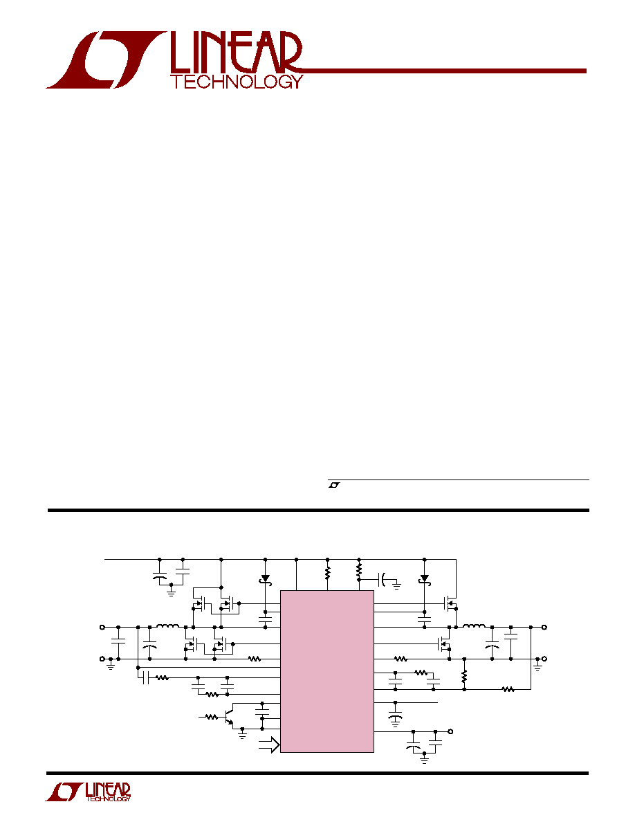
TYPICAL APPLICATIO
U
The LTC
®
1705 is a complete power supply controller for
Intel Mobile Pentium processors. It includes two switch-
ing regulator controllers, each designed to drive a pair of
N-channel MOSFETs in a voltage mode feedback, syn-
chronous buck configuration, to provide the core and I/O
supplies. The core controller includes a 5-bit DAC that
conforms to the Intel Mobile VID specification. The IC also
includes a low dropout linear regulator (LDO) that delivers
up to 150mA of output current to provide the CLK supply.
The LTC1705 uses a constant-frequency 550kHz PWM
architecture, minimizing external component size and
cost, as well as optimizing load transient performance. It
provides better than 1.25% DC accuracy at its core output,
and 2% at I/0 and CLK outputs. The high performance
feedback loops allow the circuit to keep total output
regulation within
±
5% under all transient conditions. An
open-drain PGOOD flag indicates that all three outputs are
within
±
10% of their regulated values. A shutdown circuit
disables all three outputs if the RUN/SS pin is pulled to
ground. In this mode, the LTC1705 supply current drops
to below 100
µ
A.
s
Complete Power Supply Controller for Intel
Mobile Pentium
®
Processors
s
Intel Mobile Pentium Core, I/O, Clock Supplies
s
Multiple Logic Supply Generator
, LTC and LT are registered trademarks of Linear Technology Corporation.
s
Three Regulated Outputs: Core, I/O and CLK in One
Package
s
Integrated Intel Mobile 5-Bit VID DAC
s
No External Current Sense Resistors
s
All N-Channel External MOSFET Architecture
s
550kHz Switching Frequency Minimizes External
Component Size and Cost
s
Integrated 150mA LDO Linear Regulator
s
Excellent DC Accuracy: 1.25% for Core, 2% for I/O
and CLK Supplies
s
PGOOD Flag Monitors All Three Outputs
s
High Efficiency Over Wide Load Current Range
s
Low Shutdown Current: < 100
µ
A
s
Switchers Run Out-of-Phase to Minimize C
IN
s
Small 28-Pin Narrow SSOP Package
Dual 550kHz Synchronous
Switching Regulator Controller with
5-Bit VID and 150mA LDO
Pentium is a registered trademark of Intel Corporation.
Intel Mobile Pentium VRM Supply
SWC
BGC
I
MAXC
6
4
8
SENSEC
13
R
IMAXC
, 27k
C
OUTC
180
µ
F
4V
×
6
L
C
0.68
µ
H
QBCA
QBIO
QBCB
PV
CC
PGOOD
LTC1705
VID4:0
5-BIT VID
V
CC
TGC
5
2
22
19
BOOSTC
3
+
C
OUTIO
100
µ
F
10V
×
2
+
C
IN
330
µ
F
10V
×
3
1
µ
F
V
IN
5V
V
OUTC
0.9V TO 2V
15A
+
QTCB
QTIO
C
CPC
1
µ
F
D
CPC
MBR
0520LT1
QTCA
R
IMAXI0
, 16k
L
IO
3
µ
H
V
OUTIO
1.5V
3A
V
OUTCLK
2.5V
150mA
FBC
11
R31
1.8k
R21, 11k
COMPC
10
R
PGOOD
5k
C
CPIO
1
µ
F
D
CPIO
MBR
0520LT1
10
10
µ
F
C31
1800pF
1
µ
F
C
VOUTCLK
10
µ
F
10V
C
VINCLK
10
µ
F
10V
1
µ
F
1705 TA01
+
C11
1800pF
C21
330pF
C22
100pF
1
µ
F
C12
2200pF
RB2
10k
1%
RUN/SS
9
PGND
7
C
SS
0.1
µ
F
10k
SHUTDOWN
C
IN
: KEMET T510X337K010AS
C
OUTC
: PANASONIC EEFUE0G181R
C
OUTIO
: AVX TPS0107M010R0065
L
C
: SUMIDA CEP125-4712-T007
L
IO
: SUMIDA CDRH6D28-3R0
QTCA, QTCB, QBCA, QBCB: FAIRCHILD FDS6670A
QTIO, QBIO: 1/2 FAIRCHILD NDS8926
V
INCLK
3.3V
+
GND
12
1418
SWIO
BGIO
I
MAXIO
25
28
1
COMPIO
21
TGIO
26
BOOSTIO
27
FBIO
20
V
INCLK
24
V
OUTCLK
23
R22, 11k
R12
8.87k
1%
+
LTC1705
2
Supply Voltage
V
CC
, PV
CC
, V
INCLK
.................................................. 6V
BOOSTC, BOOSTIO ............................................. 12V
BOOSTC SWC, BOOSTIO SWIO ....................... 6V
Input Voltage
SWC, SWIO ................................................ 1V to 6V
SENSEC, FBC, FBIO, VID
n ....... 0.3V to (V
CC
+ 0.3V)
PGOOD, RUN/SS,
I
MAXC
, I
MAXIO ..................................
0.3V to (V
CC
+ 0.3V)
Peak Output Current <10
µ
s
TGC, BGC .............................................................. 5A
TGIO, BGIO ....................................................... 1.25A
Operating Temperature Range (Note 2) .. 40
°
C to 85
°
C
Storage Temperature Range ................. 65
°
C to 150
°
C
Lead Temperature (Soldering, 10 sec).................. 300
°
C
ORDER PART
NUMBER
T
JMAX
= 125
°
C,
JA
= 80
°
C/W
Consult LTC Marketing for parts specified with wider operating temperature ranges.
LTC1705EGN
ABSOLUTE AXI U
RATI GS
W
W
W
U
PACKAGE/ORDER I FOR ATIO
U
U
W
ELECTRICAL CHARACTERISTICS
The
q
denotes the specifications which apply over the full operating temperature range, otherwise specifications are at T
A
= 25
°
C.
V
CC
= PV
CC
= BOOST = 5V, V
INCLK
= 3.3V unless otherwise specified. (Note 3)
1
2
3
4
5
6
7
8
9
10
11
12
13
14
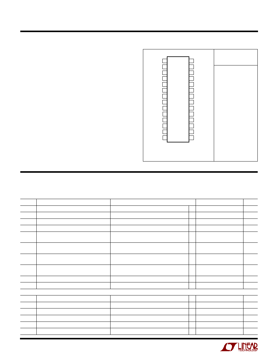
TOP VIEW
GN PACKAGE
28-LEAD PLASTIC SSOP
28
27
26
25
24
23
22
21
20
19
18
17
16
15
I
MAXIO
PV
CC
BOOSTC
BGC
TGC
SWC
PGND
I
MAXC
RUN/SS
COMPC
FBC
GND
SENSEC
VID0
BGIO
BOOSTIO
TGIO
SWIO
V
INCLK
V
OUTCLK
PGOOD
COMPIO
FBIO
V
CC
VID4
VID3
VID2
VID1
(Note 1)
SYMBOL PARAMETER
CONDITIONS
MIN
TYP
MAX
UNITS
V
CC
V
CC
Supply Voltage
q
3.15
5
5.5
V
PV
CC
PV
CC
Supply Voltage
(Note 4)
q
3.15
5
5.5
V
BV
CC
BOOST Pin Voltage
V
BOOST
V
SW
(Note 4)
q
3.15
5
5.5
V
V
INCLK
V
INCLK
Supply Voltage
q
3
3.3
5.5
V
I
VCC
V
CC
Supply Current
Test Circuit 1
q
4.5
8
mA
RUN/SS = 0V
q
40
100
µ
A
I
PVCC
PV
CC
Supply Current
V
SENSEC
= V
FBIO
= 0V, No Load at Drivers (Note 5)
q
2
6
mA
RUN/SS = 0V (Note 6)
q
1
50
µ
A
I
BOOST
I
BOOSTC
+ I
BOOSTIO
V
SENSEC
= V
FBIO
= 0V, No Load at Drivers (Note 5)
q
2
6
mA
RUN/SS = 0V (Note 6)
q
1
50
µ
A
I
VINCLK
V
INCLK
Supply Current
I
VOUTCLK
= 0mA
q
1
1.5
mA
RUN/SS = 0V
q
4
30
µ
A
V
SHDN
RUN/SS Shutdown Threshold
V
RUN/SS
(Rising Edge)
q
0.2
0.5
V
I
SS
RUN/SS Source Current
RUN/SS = 0V
3
µ
A
Core, I/O Supply Control Loops
V
SENSEC
Output Voltage Accuracy
Programmed from 0.9V to 2V
q
1.25
1.25
%
V
FBC
Core Feedback Voltage
(Note 10)
0.800
V
V
FBIO
I/O Feedback Voltage
q
0.784
0.800
0.816
V
dV
FB
Feedback Voltage Line Regulation
V
CC
= 3.3V to 5.5V
q
±
0.01
±
0.1
%/V
dV
OUT
Output Voltage Load Regulation
(Note 7)
q
0.2
0.1
%
I
FBIO
I/O Feedback Input Current
q
±
1
µ
A
LTC1705
3
ELECTRICAL CHARACTERISTICS
The
q
denotes the specifications which apply over the full operating temperature range, otherwise specifications are at T
A
= 25
°
C.
V
CC
= PV
CC
= BOOST = 5V, V
INCLK
= 3.3V unless otherwise specified. (Note 3)
SYMBOL
PARAMETER
CONDITIONS
MIN
TYP
MAX
UNITS
A
FB
Feedback Amplifier DC Gain
q
74
85
dB
GBW
Feedback Amplifier Gain Bandwidth Product
f = 100kHz (Note 7)
20
MHz
I
COMP
Feedback Amplifier Output Sink/Source Current
q
±
3
±
10
mA
V
PGOOD
Negative Power Good Threshold
Relative to Nominal Output Voltage
q
15
10
6
%
Positive Power Good Threshold
q
6
10
15
%
A
ILIM
Current Limit Amplifier DC Gain
q
40
60
dB
I
IMAX
I
MAX
Source Current
V
IMAXC
= V
IMAXIO
= 0V
q
12
10
8
µ
A
Core, I/O Supply Switching Characteristics
f
OSC
Oscillator Frequency
Test Circuit 1
q
460
550
650
kHz
OSC
Core and I/O Oscillator Phase Difference
(Note 7)
180
DEG
DC
MAX
Maximum Duty Cycle
q
87
90
93
%
t
NOV
Driver Nonoverlap
Test Circuit 1, 50% to 50%
q
10
25
120
ns
t
r
, t
f
Driver Rise/Fall Time
Test Circuit 1, 10% to 90%
q
15
100
ns
Clock Supply Output
V
OUTCLK
CLK Output Voltage
I
VOUTCLK
= 0mA
q
2.45
2.50
2.55
V
dV
OUTCLK
Output Voltage Line Regulation
V
INCLK
= 3.0V to 5.5V
q
±
0.02
±
0.1
%/V
Output Voltage Load Regulation
I
VOUTCLK
= 0mA to 150mA
q
0.1
0.05
%
ILM
CLK
CLK Output Short-Circuit Current
I
VOUTCLK
= 0V
q
240
150
mA
V
DROPOUT
CLK Output Dropout Voltage
I
VOUTCLK
= 150mA, d
VOUTCLK
= 1% (Note 8)
q
0.3
0.5
V
V
PGOOD
Negative V
OUTCLK
Power Good Threshold
Relative to V
OUTCLK
q
15
10
6
%
Positive V
OUTCLK
Power Good Threshold
Relative to V
OUTCLK
q
6
10
15
%
VID Inputs
R1
Resistance Across SENSEC and FBC
10
k
R
VID
VID Input Pull-Up Resistance
(Note 9)
30
k
V
VID
VID Input Threshold
q
0.4
1.6
V
PGOOD
I
PGOOD
V
PGOOD
Sink Current
Power Good
q
10
µ
A
Power Bad
q
10
mA
V
OLPG
PGOOD Output Low Voltage
I
PGOOD
= 1mA
q
0.03
0.1
V
T
PGOOD
V
PGOOD
Falling Edge Delay
q
2
4
8
µ
s
V
PGOOD
Rising Edge Delay
q
10
20
40
µ
s
V
PBAD
Pulse
VID Code Change
q
10
20
40
µ
s
Note 1: Absolute Maximum Ratings are those values beyond which the life
of a device may be impaired.
Note 2: The LTC1705 is guaranteed to meet performance specifications
from 0
°
C to 70
°
C. Specifications over the 40
°
C to 85
°
C operating
temperature range are assured by design, characterization and correlation
with statistical process controls.
Note 3: All currents into device pins are positive; all currents out of device
pins are negative. All voltages are referenced to ground unless otherwise
specified.
Note 4: PV
CC
and BV
CC
(V
BOOST
V
SW
) must be greater than V
GS(ON)
of
the external MOSFETs to ensure proper operation.
Note 5: Supply current in normal operation is dominated by the current
needed to charge and discharge the capacitance of the external MOSFET
gates. This current varies with supply voltage and the choice of external
MOSFETs.
Note 6: Supply current in shutdown is dominated by external MOSFET
leakage and may be significantly higher than the quiescent current drawn
by the LTC1705, especially at elevated temperature.
Note 7: Guaranteed by design, not subject to test.
Note 8: Dropout voltage is the minimum input-to-output voltage
differential required to maintain regulation at the specified output current.
In dropout, the output voltage will be equal to V
INCLK
V
DROPOUT
.
Note 9: Each internal pull-up resistor attached to the VID inputs has a
series diode connected to V
CC
to allow input voltages higher than the V
CC
supply without damage or clamping. (See Block Diagram.)
Note 10: The core feedback voltage accuracy is guaranteed by the V
SENSE
output voltage accuracy test.
LTC1705
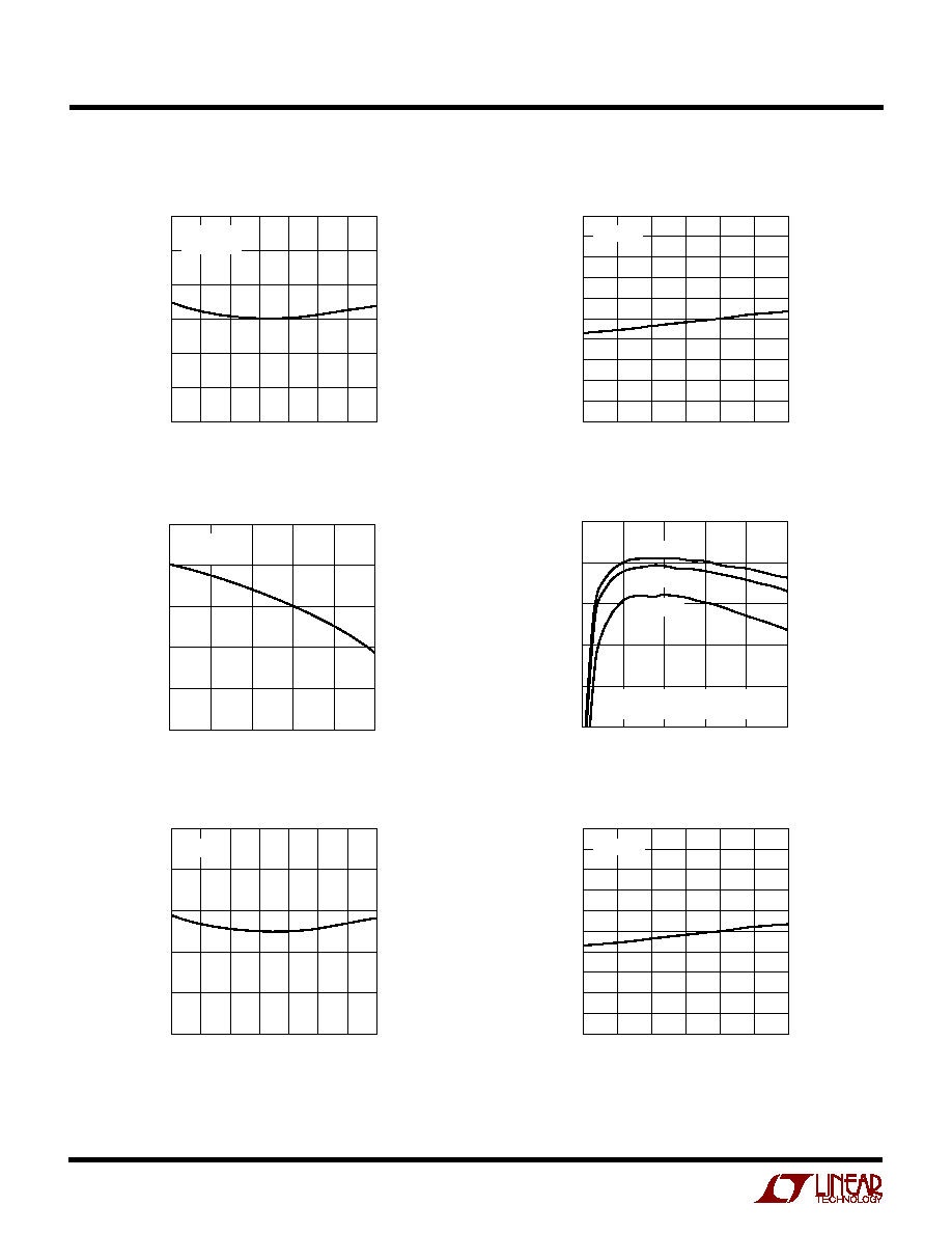
4
TEMPERATURE (
°
C)
50
25
0
25
50
75
100
125
V
SENSEC
(V)
1705 G01
1.315
1.310
1.305
1.300
1.295
1.290
1.285
V
CC
= 5V
V
OUT
= 1.3V
V
CC
(V)
3
3.5
4
4.5
5
5.5
6
V
SENSEC
(mV)
1705 G02
1.30
1.04
0.78
0.52
0.26
0
0.26
0.52
0.78
1.04
1.30
V
SENSE
(%)
0.10
0.08
0.06
0.04
0.02
0
0.02
0.04
0.06
0.08
0.10
T
A
= 25
°
C
I
LOAD
(A)
0
3
6
9
12
15
V
SENSEC
(mV)
1705 G03
0.8
0
0.8
1.6
2.4
3.2
V
SENSE
(%)
0.05
0
0.05
0.10
0.15
0.20
T
A
= 25
°
C
V
OUT
= 1.6V
I
LOAD
(A)
0
3
6
9
12
15
EFFICIENCY (%)
1705 G04
100
90
80
70
60
50
V
IN
= 5V, T
A
= 25
°
C, I/O DISABLED
QTC = QBC = 2
×
FDS6670A
V
OUT
= 2V
V
OUT
= 1.6V
V
OUT
= 0.9V
TEMPERATURE (
°
C)
50
25
0
25
50
75
100
125
V
FBIO
(V)
1705 G05
0.810
0.806
0.802
0.798
0.794
0.790
V
CC
= 5V
V
CC
(V)
3
3.5
4
4.5
5
5.5
6
V
FBIO
(mV)
1705 G06
0.80
0.64
0.48
0.32
0.16
0
0.16
0.32
0.48
0.64
0.80
V
FBIO
(%)
0.10
0.08
0.06
0.04
0.02
0
0.02
0.04
0.06
0.08
0.10
T
A
= 25
°
C
TYPICAL PERFOR A CE CHARACTERISTICS
U
W
V
SENSEC
vs Temperature
V
SENSEC
Line Regulation
V
SENSEC
Load Regulation
Core Supply Efficiency
V
FBIO
vs Temperature
V
FBIO
Line Regulation
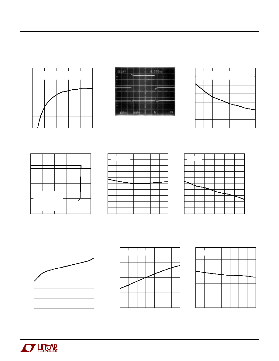
LTC1705
5
I
LOAD
(A)
0
0.5
1
1.5
2
2.5
EFFICIENCY (%)
1705 G07
100
90
80
70
60
50
V
IN
= 5V, V
OUT
= 1.5V, T
A
= 25
°
C,
CORE DISABLED, QTIO = QBIO = NDS8926
TEMPERATURE (
°
C)
50
25
0
25
50
75
100
125
CURRENT LIMIT THRESHOLD (A)
1705 G09
24
22
20
18
16
14
12
10
V
IN
= 5V, V
OUT
= 1.6V,
V
OUT
= 1%,
R
IMAXC
= 24.9k, QTC = QBC = 2
×
FDS6670A
LOAD CURRENT (A)
0
4
8
12
16
20
V
OUTC
(V)
1705 G10
2.0
1.5
1.0
0.5
0
T
A
= 25
°
C, V
IN
= 5V,
V
OUT
= 1.6V,
QBC = 2
×
FDS6670A,
R
IMAXC
= 24.9k,
C
RUNSS
= 0.01
µ
F
TEMPERATURE (
°
C)
50
25
0
25
50
75
100
125
V
OUTCLK
(V)
1705 G11
2.55
2.54
2.53
2.52
2.51
2.50
2.49
2.48
2.47
2.46
2.45
V
INCLK
= 3.3V
V
INCLK
(V)
3
3.5
4
4.5
5
5.5
6
V
OUTCLK
(mV)
1705 G12
2.5
2.0
1.5
1.0
0.5
0
0.5
1.0
1.5
2.0
2.5
V
OUTCLK
(%)
0.10
0.08
0.06
0.04
0.02
0
0.02
0.04
0.06
0.08
0.10
T
A
= 25
°
C
V
OUTCLK
(mV)
1705 G13
0.5
0
0.5
1.0
1.5
2.0
2.5
V
OUTCLK
(%)
0.02
0
0.02
0.04
0.06
0.08
0.10
I
OUTCLK
(mA)
150
125
100
75
50
25
0
T
A
= 25
°
C
TEMPERATURE (
°
C)
50
25
0
25
50
75
100
125
V
DROPOUT
(mV)
1705 G14
500
450
400
350
300
250
200
150
100
I
OUTCLK
= 150mA
TEMPERATURE (
°
C)
50
25
0
25
50
75
100
125
ILM
CLK
(mA)
1705 G15
150
190
230
270
310
350
V
INCLK
= 3.3V
TYPICAL PERFOR A CE CHARACTERISTICS
U
W
I/O Supply Efficiency
V
OUTC
0A To 10A Load Step
Current Limit Threshold vs
Temperature
0A TO 10A
LOAD
5A/DIV
V
OUT
= 1.6V
AC 50mV/
DIV
5ms/DIV
1705 G08
V
OUTC
vs Load Current
V
OUTCLK
vs Temperature
V
OUTCLK
Line Regulation
V
OUTCLK
Load Regulation
V
OUTCLK
Dropout Voltage vs
Temperature
V
OUTCLK
Short-Circuit Current vs
Temperature