Äîêóìåíòàöèÿ è îïèñàíèÿ www.docs.chipfind.ru
1
LTC1751/LTC1751-3.3/LTC1751-5
APPLICATIO S
U
FEATURES
DESCRIPTIO
U
TYPICAL APPLICATIO
U
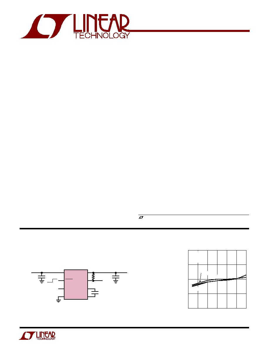
Micropower, Regulated
Charge Pump
DC/DC Converters
s
5V Output Current: 100mA (V
IN
3V)
s
3.3V Output Current: 80mA (V
IN
2.5V)
s
Ultralow Power: 20
µ
A Quiescent Current
s
Regulated Output Voltage: 3.3V
±
4%, 5V
±
4%, ADJ
s
No Inductors
s
Short-Circuit/Thermal Protection
s
V
IN
Range: 2V to 5.5V
s
800kHz Switching Frequency
s
Very Low Shutdown Current: <2
µ
A
s
Shutdown Disconnects Load from V
IN
s
PowerGood/Undervoltage Output
s
Adjustable Soft-Start Time
s
Available in an 8-Pin MSOP Package
s
Li-Ion Battery Backup Supplies
s
Local 3V and 5V Conversion
s
Smart Card Readers
s
PCMCIA Local 5V Supplies
s
White LED Backlighting
The LTC
®
1751 family are micropower charge pump DC/
DC converters that produce a regulated output voltage at
up to 100mA. The input voltage range is 2V to 5.5V.
Extremely low operating current (20
µ
A typical with no
load) and low external parts count (one flying capacitor
and two small bypass capacitors at V
IN
and V
OUT
) make
them ideally suited for small, battery-powered applica-
tions.
The LTC1751 family operate as Burst Mode
TM
switched
capacitor voltage doublers to achieve ultralow quiescent
current. They have thermal shutdown capability and can
survive a continuous short circuit from V
OUT
to GND. The
PGOOD pin on the LTC1751-3.3 and LTC1751-5 indicates
when the output voltage has reached its final value and if
the output has an undervoltage fault condition. The FB pin
of the adjustable LTC1751 can be used to program the
desired output voltage or current. An optional soft-start
capacitor may be used at the SS pin to prevent excessive
inrush current during start-up.
The LTC1751 family is available in an 8-pin MSOP
package.
, LTC and LT are registered trademarks of Linear Technology Corporation.
Burst Mode is a trademark of Linear Technology Corporation.
V
IN
SHDN
SS
GND
2
1
6
5
3
7
8
4
V
OUT
PGOOD
C
+
C
LTC1751-5
V
OUT
5V
±
4%
I
OUT
100mA, V
IN
3V
I
OUT
50mA, V
IN
2.7V
V
IN
2.7V
TO 5.5V
C2
10
µ
F
C
FLY
1
µ
F
PGOOD
R1
100k
OFF ON
1751 TA01
C1
10
µ
F
C
FLY
= MURATA GRM39X5R105K6.3AJ
C1, C2 = MURATA GRM40X5R106K6.3AJ
Regulated 5V Output from a 2.7V to 5.5V Input
Output Voltage vs Input Voltage
INPUT VOLTAGE (V)
2.5
4.8
OUTPUT VOLTAGE (V)
4.9
5.0
5.1
5.2
3.0
3.5
4.0
4.5
1751 TA02
5.0
5.5
I
OUT
= 50mA
C
FLY
= 1
µ
F
C
OUT
= 10
µ
F
T
A
= 25
°
C
T
A
= 40
°
C
T
A
= 85
°
C
2
LTC1751/LTC1751-3.3/LTC1751-5
ORDER PART
NUMBER
LTC1751EMS8
LTC1751EMS8-3.3
LTC1751EMS8-5
T
JMAX
= 150
°
C,
JA
= 160
°
C/W
*PGOOD ON LTC1751-3.3/LTC1751-5
FB ON LTC1751
Consult factory for parts specified with wider operating temperature ranges.
The
q
denotes specifications which apply over the full specified
temperature range, otherwise specifications are at T
A
= 25
°
C. C
FLY
= 1
µ
F, C
IN
= 10
µ
F, C
OUT
= 10
µ
F unless otherwise noted.
(Note 1)
V
IN
to GND .................................................. 0.3V to 6V
PGOOD, FB, V
OUT
to GND ........................... 0.3V to 6V
SS, SHDN to GND ........................ 0.3V to (V
IN
+ 0.3V)
V
OUT
Short-Circuit Duration ............................. Indefinite
I
OUT
(Note 2)....................................................... 125mA
Operating Temperature Range (Note 3) .. 40
°
C to 85
°
C
Storage Temperature Range ................ 65
°
C to 150
°
C
Lead Temperature (Soldering, 10 sec)................. 300
°
C
ABSOLUTE AXI U RATI GS
W
W
W
U
PACKAGE/ORDER I FOR ATIO
U
U
W
ELECTRICAL CHARACTERISTICS
1
2
3
4
FB/PGOOD*
V
OUT
V
IN
GND
8
7
6
5
SS
SHDN
C
+
C
TOP VIEW
MS8 PACKAGE
8-LEAD PLASTIC MSOP
MS8 PART MARKING
LTKL
LTKN
LTKP
SYMBOL
PARAMETER
CONDITIONS
MIN
TYP
MAX
UNITS
LTC1751-3.3
V
IN
Input Supply Voltage
q
2
4.4
V
V
OUT
Output Voltage
2V
V
IN
4.4V, I
OUT
40mA
q
3.17
3.3
3.43
V
2.5V
V
IN
4.4V, I
OUT
80mA
q
3.17
3.3
3.43
V
I
CC
Operating Supply Current
2V
V
IN
4.4V, I
OUT
= 0mA, SHDN = V
IN
q
18
40
µ
A
V
R
Output Ripple
V
IN
= 2.5V, I
OUT
= 40mA
68
mV
P-P
Efficiency
V
IN
= 2V, I
OUT
= 40mA
80
%
LTC1751-5
V
IN
Input Supply Voltage
q
2.7
5.5
V
V
OUT
Output Voltage
2.7V
V
IN
5.5V, I
OUT
50mA
q
4.8
5
5.2
V
3V
V
IN
5.5V, I
OUT
100mA
q
4.8
5
5.2
V
I
CC
Operating Supply Current
2.7V
V
IN
5.5V, I
OUT
= 0mA, SHDN = V
IN
q
20
50
µ
A
V
R
Output Ripple
V
IN
= 3V, I
OUT
= 50mA
75
mV
P-P
Efficiency
V
IN
= 3V, I
OUT
= 50mA
82
%
LTC1751
V
IN
Input Supply Voltage
q
2
5.5
V
I
CC
Operating Supply Current
2V
V
IN
5.5V, I
OUT
= 0mA, SHDN = V
IN
(Note 4 )
q
16
40
µ
A
V
FB
FB Regulation Voltage
2V
V
IN
5.5V, I
OUT
20mA
q
1.157
1.205
1.253
V
I
FB
FB Input Current
V
FB
= 1.3V
q
50
50
nA
R
OUT
Open-Loop Charge Pump Strength
V
IN
= 2V, V
OUT
= 3.3V (Note 5)
q
8.5
20
V
IN
= 2.7V, V
OUT
= 5V (Note 5)
q
6.0
12
3
LTC1751/LTC1751-3.3/LTC1751-5
The
q
denotes specifications which apply over the full specified
temperature range, otherwise specifications are at T
A
= 25
°
C. C
FLY
= 1
µ
F, C
IN
= 10
µ
F, C
OUT
= 10
µ
F unless otherwise noted.
ELECTRICAL CHARACTERISTICS
Note 1: Absolute Maximum Ratings are those values beyond which the life
of a device may be impaired.
Note 2: Based on long term current density limitations.
Note 3: The LTC1751EMS8-X is guaranteed to meet performance
specifications from 0
°
C to 70
°
C. Specifications over the 40
°
C to 85
°
C
operating temperature range are assured by design, characterization and
correlation with statistical process controls.
Note 4: The no load input current will be approximately I
CC
plus twice the
standing current in the resistive output divider.
Note 5: R
OUT
(2V
IN
V
OUT
)/I
OUT
.
Note 6: See Figure 2.
TYPICAL PERFOR A CE CHARACTERISTICS
U
W
Output Voltage vs Load Current
LOAD CURRENT (mA)
0
3.20
OUTPUT VOLTAGE (V)
3.25
3.30
3.35
3.40
25
50
75
100
1751 G01
125
150
T
A
= 25
°
C
C
FLY
= 1
µ
F
V
IN
= 2V
V
IN
= 2.5V
INPUT VOLTAGE (V)
2.0
OUTPUT VOLTAGE (V)
3.30
3.35
4.0
1751 G02
3.25
3.20
2.5
3.0
3.5
4.5
3.40
I
OUT
= 40mA
C
FLY
= 1
µ
F
C
OUT
= 10
µ
F
T
A
= 40
°
C
T
A
= 85
°
C
T
A
= 25
°
C
INPUT VOLTAGE (V)
2.0
SUPPLY CURRENT (
µ
A)
20
30
4.0
1751 G03
10
0
2.5
3.0
3.5
4.5
40
I
OUT
= 0mA
C
FLY
= 1
µ
F
V
SHDN
= V
IN
T
A
= 85
°
C
T
A
= 25
°
C
T
A
= 40
°
C
Output Voltage vs Input Voltage
No Load Supply Current
vs Input Voltage
(LTC1751-3.3)
SYMBOL
PARAMETER
CONDITIONS
MIN
TYP
MAX
UNITS
LTC1751-3.3/LTC1751-5
UVL
PGOOD Undervoltage Low Threshold
Relative to Regulated V
OUT
(Note 6)
q
11
7
3
%
UVH
PGOOD Undervoltage High Threshold
Relative to Regulated V
OUT
(Note 6)
q
8
4.5
2
%
V
OL
PGOOD Low Output Voltage
I
PGOOD
= 500
µ
A
q
0.4
V
I
OH
PGOOD High Output Leakage
V
PGOOD
= 5.5V
q
1
µ
A
LTC1751/LTC1751-3.3/LTC1751-5
I
SHDN
Shutdown Supply Current
V
IN
3.6V, V
OUT
= 0V, V
SHDN
= 0V
q
0.01
2
µ
A
3.6V < V
IN
, V
OUT
= 0V, V
SHDN
= 0V
q
5
µ
A
V
IH
SHDN Input Threshold (High)
q
1.5
V
V
IL
SHDN Input Threshold (Low)
q
0.3
V
I
IH
SHDN Input Current (High)
SHDN = V
IN
q
1
1
µ
A
I
IL
SHDN Input Current (Low)
SHDN = 0V
q
1
1
µ
A
t
r
V
OUT
Rise Time
V
IN
= 3V, I
OUT
= 0mA, 10% to 90% (Note 6)
0.6ms/nF · C
SS
sec
f
OSC
Switching Frequency
Oscillator Free Running
800
kHz
4
LTC1751/LTC1751-3.3/LTC1751-5
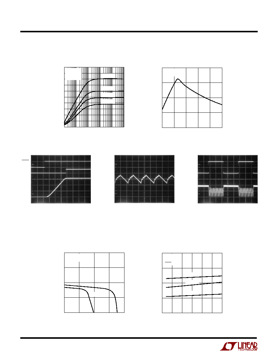
TYPICAL PERFOR A CE CHARACTERISTICS
U
W
Power Efficiency vs Load Current
Short-Circuit Output Current
vs Input Voltage
LOAD CURRENT (mA)
0.001
40
EFFICIENCY (%)
50
60
70
80
0.01
0.1
1
10
100
1751 G04
30
20
10
0
90
100
V
IN
= 2.75V
V
IN
= 2V
V
IN
= 4.4V
V
IN
= 3.3V
T
A
= 25
°
C
C
FLY
= 1
µ
F
C
OUT
= 10
µ
F
INPUT VOLTAGE (V)
2.0
OUTPUT CURRENT (mA)
150
200
4.0
1751 G05
100
50
2.5
3.0
3.5
4.5
250
T
A
= 25
°
C
C
FLY
= 1
µ
F
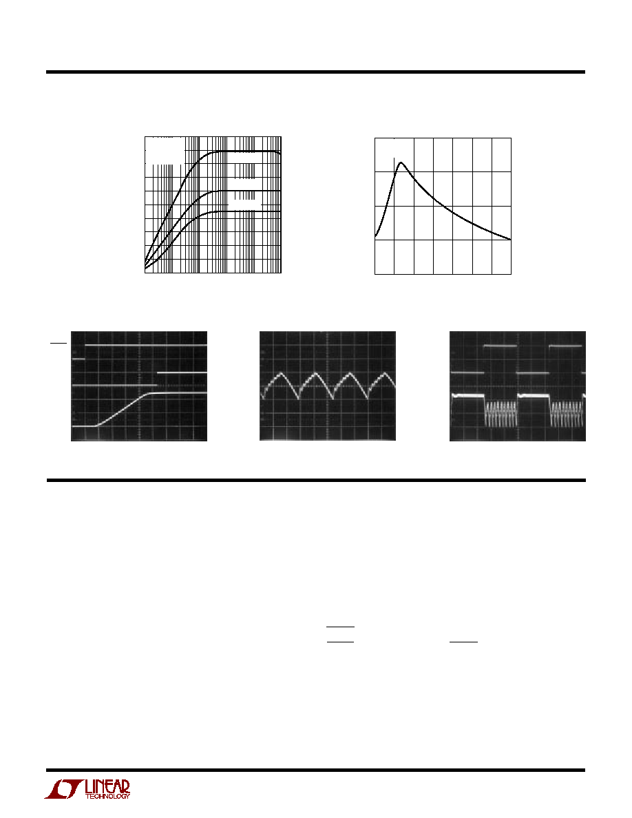
Start-Up
C
SS
= 10nF
2ms/DIV
1751 G06
SHDN
2V/DIV
PGOOD
5V/DIV
V
OUT
1V/DIV
Output Ripple
V
IN
= 2.5V
5
µ
s/DIV
1751 G07
I
OUT
= 80mA
C
OUT
= 10
µ
F
V
OUT
AC COUPLED
50mV/DIV
Load Transient Response
V
IN
= 2.5V
50
µ
s/DIV
1751 G08
V
OUT
AC COUPLED
50mV/DIV
I
OUT
40mA/DIV
(LTC1751-3.3)
(LTC1751-5)
OUTPUT CURRENT (mA)
0
OUTPUT VOLTAGE (V)
5.0
5.1
200
1751 G09
4.9
4.8
50
100
150
V
IN
= 3V
5.2
T
A
= 25
°
C
C
FLY
= 1
µ
F
V
IN
= 2.7V
Output Voltage vs Output Current
No Load Supply Current
vs Input Voltage
INPUT VOLTAGE (V)
2.5
0
SUPPLY CURRENT (
µ
A)
10
20
30
40
3.0
3.5
4.0
4.5
1751 G10
5.0
5.5
C
FLY
= 1
µ
F
I
OUT
= 0
V
SHDN
= V
IN
T
A
= 85
°
C
T
A
= 25
°
C
T
A
= 40
°
C
5
LTC1751/LTC1751-3.3/LTC1751-5
U
U
U
PI FU CTIO S
PGOOD (Pin 1) (LTC1751-3.3/LTC1751-5): Output Volt-
age Status Indicator. On start-up, this open-drain pin re-
mains low until the output voltage, V
OUT
, is within 4.5%
(typ) of its final value. Once V
OUT
is valid, PGOOD becomes
high-Z. If, due to a fault condition, V
OUT
falls 7% (typ) below
its correct regulation level, PGOOD pulls low. PGOOD may
be pulled up through an external resistor to any appropri-
ate reference level.
FB (Pin 1) (LTC1751): The voltage on this pin is compared
to the internal reference voltage (1.205V) by the error
comparator to keep the output in regulation. An external
resistor divider is required between V
OUT
and FB to pro-
gram the output voltage.
V
OUT
(Pin 2): Regulated Output Voltage. For best perfor-
mance, V
OUT
should be bypassed with a 6.8
µ
F (min) low
ESR capacitor as close to the pin as possible .
V
IN
(Pin 3): Input Supply Voltage. V
IN
should be bypassed
with a 6.8
µ
F (min) low ESR capacitor.
GND (Pin 4): Ground. Should be tied to a ground plane for
best performance.
C
(Pin 5): Flying Capacitor Negative Terminal.
C
+
(PIN 6): Flying Capacitor Positive Terminal.
SHDN (Pin 7): Active Low Shutdown Input. A low on
SHDN disables the device. SHDN must not be allowed to
float.
SS (Pin 8): Soft-Start Programming Pin. A capacitor on SS
programs the start-up time of the charge pump so that
large start-up input current is eliminated.
TYPICAL PERFOR A CE CHARACTERISTICS
U
W
Power Efficiency vs Load Current
Short-Circuit Output Current
vs Input Voltage
Start-Up
C
SS
= 10nF
2ms/DIV
1751 G13
SHDN
2V/DIV
PGOOD
5V/DIV
V
OUT
2V/DIV
Output Ripple
V
IN
= 3V
5
µ
s/DIV
1751 G14
I
OUT
= 100mA
C
OUT
= 10
µ
F
V
OUT
AC COUPLED
50mV/DIV
Load Transient Response
V
IN
= 3V
50
µ
s/DIV
1751 G15
V
OUT
AC COUPLED
50mV/DIV
I
OUT
50mA/DIV
(LTC1751-5)
LOAD CURRENT (mA)
0.001
40
EFFICIENCY (%)
50
60
70
80
0.01
0.1
1
10
100
1751 G11
30
20
10
0
90
100
V
IN
= 2.7V
V
IN
= 4.1V
V
IN
= 5.5V
T
A
= 25
°
C
C
FLY
= 1
µ
F
C
OUT
= 10
µ
F
INPUT VOLTAGE (V)
2.0
50
OUTPUT CURRENT (mA) 100
150
200
250
2.5
3.0
3.5
4.0
1751 G12
4.5
5.0
5.5
T
A
= 25
°
C
C
FLY
= 1
µ
F