 | –≠–ª–µ–∫—Ç—Ä–æ–Ω–Ω—ã–π –∫–æ–º–ø–æ–Ω–µ–Ω—Ç: LTC1864 | –°–∫–∞—á–∞—Ç—å:  PDF PDF  ZIP ZIP |

LTC1863/LTC1867
1
18637f
APPLICATIO S
U
BLOCK DIAGRA
W
FEATURES
DESCRIPTIO
U
s
Industrial Process Control
s
High Speed Data Acquisition
s
Battery Operated Systems
s
Multiplexed Data Acquisition Systems
s
Imaging Systems
s
Sample Rate: 200ksps
s
16-Bit No Missing Codes and
±
2LSB Max INL
s
8-Channel Multiplexer with:
Single Ended or Differential Inputs and
Unipolar or Bipolar Conversion Modes
s
SPI/MICROWIRE
TM
Serial I/O
s
Signal-to-Noise Ratio: 89dB
s
Single 5V Operation
s
On-Chip or External Reference
s
Low Power: 1.3mA at 200ksps, 0.76mA at 100ksps
s
Sleep Mode
s
Automatic Nap Mode Between Conversions
s
16-Pin Narrow SSOP Package
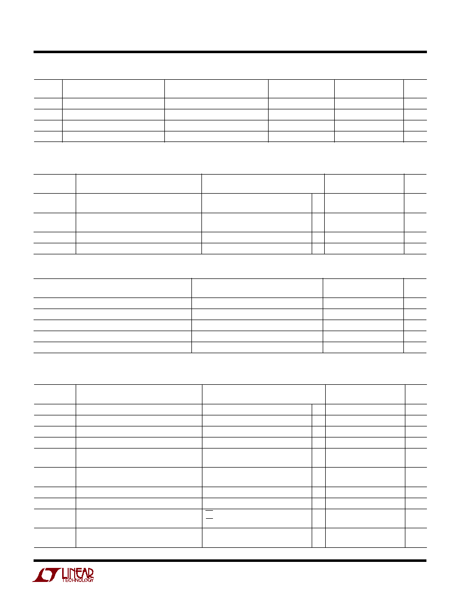
12-/16-Bit, 8-Channel
200ksps ADCs
The LTC
Æ
1863/LTC1867 are pin-compatible, 8-channel
12-/16-bit A/D converters with serial I/O, and an internal
reference. The ADCs typically draw only 1.3mA from a
single 5V supply.
The 8-channel input multiplexer can be configured for
either single-ended or differential inputs and unipolar
or bipolar conversions (or combinations thereof). The
automatic nap and sleep modes benefit power sensitive
applications.
The LTC1867's DC performance is outstanding with a
±
2LSB INL specification and no missing codes over tem-
perature. The signal-to-noise ratio (SNR) for the LTC1867
is typically 89dB, with the internal reference.
Housed in a compact, narrow 16-pin SSOP package, the
LTC1863/LTC1867 can be used in space-sensitive as well
as low-power applications.
, LTC and LT are registered trademarks of Linear Technology Corporation.
CH0
CH1
CH2
CH3
CH4
CH5
CH6
CH7/COM
1
2
3
4
5
6
7
8
16
15
14
13
12
11
10
V
DD
GND
SDI
SDO
SCK
CS/CONV
V
REF
18637 BD
12-/16-BIT
200ksps
ADC
+
≠
SERIAL
PORT
ANALOG
INPUT
MUX
REFCOMP
9
INTERNAL
2.5V REF
LTC1863/LTC1867
MICROWIRE is a trademark of National Semiconductor Corp.
OUTPUT CODE
0
INL (LBS)
49152
18637 GO1
16384
32768
65536
2.0
1.5
1.0
0.5
0
≠ 0.5
≠ 1.0
≠ 1.5
≠ 2.0
Integral Nonlinearity vs Output Code
(LTC1867)

LTC1863/LTC1867
2
18637f
TOP VIEW
GN PACKAGE
16-LEAD NARROW PLASTIC SSOP
1
2
3
4
5
6
7
8
16
15
14
13
12
11
10
9
CH0
CH1
CH2
CH3
CH4
CH5
CH6
CH7/COM
V
DD
GND
SDI
SDO
SCK
CS/CONV
V
REF
REFCOMP
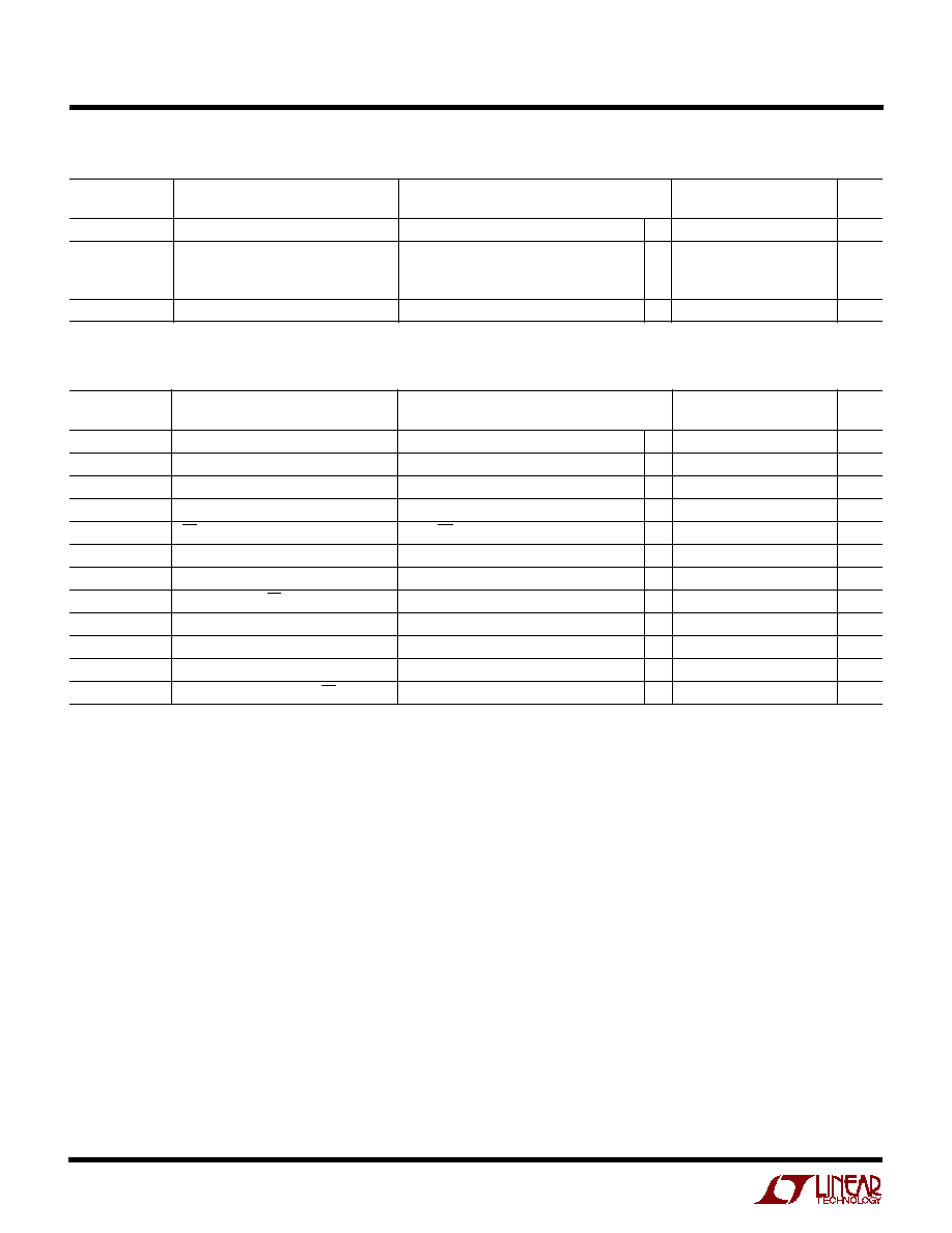
CO VERTER CHARACTERISTICS
U
Supply Voltage (V
DD
) ................................... ≠0.3V to 6V
Analog Input Voltage
CH0-CH7/COM (Note 3) .......... ≠ 0.3V to (V
DD
+ 0.3V)
V
REF
, REFCOMP (Note 4)......... ≠ 0.3V to (V
DD
+ 0.3V)
Digital Input Voltage (SDI, SCK, CS/CONV)
(Note 4) .................................................≠ 0.3V to 10V
Digital Output Voltage (SDO) ....... ≠ 0.3V to (V
DD
+ 0.3V)
Power Dissipation .............................................. 500mW
Operating Temperature Range
LTC1863C/LTC1867C/LTC1867AC .......... 0
∞
C to 70
∞
C
LTC1863I/LTC1867I/LTC1867AI ........ ≠ 40
∞
C to 85
∞
C
Storage Temperature Range ................. ≠ 65
∞
C to 150
∞
C
Lead Temperature (Soldering, 10 sec).................. 300
∞
C
ORDER PART
NUMBER
T
JMAX
= 110
∞
C,
JA
= 95
∞
C/W
LTC1863CGN
LTC1863IGN
LTC1867CGN
LTC1867IGN
LTC1867ACGN
LTC1867AIGN
ABSOLUTE AXI U
RATI GS
W
W
W
U
PACKAGE/ORDER I FOR ATIO
U
U
W
(Notes 1, 2)
The
q
denotes the specifications which apply over the full operating
temperature range, otherwise specifications are at T
A
= 25
∞
C. With external reference (Notes 5, 6)
LTC1863
LTC1867
LTC1867A
PARAMETER
CONDITIONS
MIN
TYP
MAX
MIN
TYP
MAX
MIN
TYP
MAX
UNITS
Resolution
q
12
16
16
Bits
No Missing Codes
q
12
15
16
Bits
Integral Linearity Error
Unipolar (Note 7)
q
±
1
±
4
±
2
LSB
Bipolar
q
±
1
±
4
±
2.5
LSB
Differential Linearity Error
q
±
1
≠2
3
≠1
1.75
LSB
Transition Noise
0.1
0.74
0.74
LSB
RMS
Offset Error
Unipolar (Note 8)
q
±
3
±
32
±
32
LSB
Bipolar
q
±
4
±
64
±
64
LSB
Offset Error Match
Unipolar
±
1
±
2
±
2
LSB
Bipolar
±
1
±
2
±
2
LSB
Offset Error Drift
±
0.5
±
0.5
±
0.5
ppm/
∞
C
Gain Error
Unipolar
±
6
±
96
±
64
LSB
Bipolar
±
6
±
96
±
64
LSB
Gain Error Match
±
1
±
4
±
2
LSB
Gain Error Tempco
Internal Reference
±
15
±
15
±
15
ppm/
∞
C
External Reference
±
2.7
±
2.7
±
2.7
ppm/
∞
C
Power Supply Sensitivity
V
DD
= 4.75V ≠ 5.25V
±
1
±
5
±
5
LSB
Consult LTC Marketing for parts specified with wider operating temperature ranges.
GN PART MARKING
1863
1867
(Note 5)
DY
A
IC ACCURACY
U
W
LTC1863
LTC1867/LTC1867A
SYMBOL
PARAMETER
CONDITIONS
MIN
TYP
MAX
MIN
TYP
MAX
UNITS
SNR
Signal-to-Noise Ratio
1kHz Input Signal
73.6
89
dB
S/(N+D)
Signal-to-(Noise + Distortion) Ratio
1kHz Input Signal
73.5
88
dB
LTC1863/LTC1867
3
18637f
DY
A
IC ACCURACY
U
W
A ALOG I PUT
U
U
I TER AL REFERE CE CHARACTERISTICS
U
U
U
DIGITAL I PUTS A D DIGITAL OUTPUTS
U
U
LTC1863
LTC1867/LTC1867A
SYMBOL
PARAMETER
CONDITIONS
MIN
TYP
MAX
MIN
TYP
MAX
UNITS
THD
Total Harmonic Distortion
1kHz Input Signal, Up to 5th Harmonic
≠94.5
≠ 95
dB
Peak Harmonic or Spurious Noise
1kHz Input Signal
≠94.5
≠ 95
dB
Channel-to-Channel Isolation
100kHz Input Signal
≠100
≠117
dB
Full Power Bandwidth
≠3dB Point
1.25
1.25
MHz
(Note 5)
The
q
denotes the specifications which apply over the
full operating temperature range, otherwise specifications are at T
A
= 25
∞
C. (Note 5)
(Note 5)
SYMBOL
PARAMETER
CONDITIONS
MIN
TYP
MAX
UNITS
Analog Input Range
Unipolar Mode (Note 9)
q
0-4.096
V
Bipolar Mode
q
±
2.048
V
C
IN
Analog Input Capacitance for CH0 to
Between Conversions (Sample Mode)
32
pF
CH7/COM
During Conversions (Hold Mode)
4
pF
t
ACQ
Sample-and-Hold Acquisition Time
q
1.5
1.1
µ
s
Input Leakage Current
On Channels, CHX = 0V or V
DD
q
±
1
µ
A
PARAMETER
CONDITIONS
MIN
TYP
MAX
UNITS
V
REF
Output Voltage
I
OUT
= 0
2.480
2.500
2.520
V
V
REF
Output Tempco
I
OUT
= 0
±
15
ppm/
∞
C
V
REF
Line Regulation
4.75V
V
DD
5.25V
0.43
mV/V
V
REF
Output Resistance
I
OUT
0.1mA
6
k
REFCOMP Output Voltage
I
OUT
= 0
4.096
V
SYMBOL
PARAMETER
CONDITIONS
MIN
TYP
MAX
UNITS
V
IH
High Level Input Voltage
V
DD
= 5.25V
q
2.4
V
V
IL
Low Level Input Voltage
V
DD
= 4.75V
q
0.8
V
I
IN
Digital Input Current
V
IN
= 0V to V
DD
q
±
10
µ
A
C
IN
Digital Input Capacitance
2
pF
V
OH
High Level Output Voltage (SDO)
V
DD
= 4.75V, I
O
= ≠10
µ
A
4.75
V
V
DD
= 4.75V, I
O
= ≠200
µ
A
q
4
4.74
V
V
OL
Low Level Output Voltage (SDO)
V
DD
= 4.75V, I
O
= 160
µ
A
0.05
V
V
DD
= 4.75V, I
O
= 1.6mA
q
0.10
0.4
V
I
SOURCE
Output Source Current
SDO = 0V
≠32
mA
I
SINK
Output Sink Current
SDO = V
DD
19
mA
Hi-Z Output Leakage
CS/CONV = High, SDO = 0V or V
DD
q
±
10
µ
A
Hi-Z Output Capacitance
CS/CONV = High (Note 10)
q
15
pF
Data Format
Unipolar
Straight Binary
Bipolar
Two's Complement
The
q
denotes the specifications which apply over the full operating temperature range, otherwise
specifications are at T
A
= 25
∞
C. (Note 5)
LTC1863/LTC1867/LTC1867A
LTC1863/LTC1867/LTC1867A
LTC1863/LTC1867/LTC1867A
LTC1863/LTC1867
4
18637f
SYMBOL
PARAMETER
CONDITIONS
MIN
TYP
MAX
UNITS
V
DD
Supply Voltage
(Note 9)
4.75
5.25
V
I
DD
Supply Current
f
SAMPLE
= 200ksps
q
1.3
1.8
mA
NAP Mode
150
µ
A
SLEEP Mode
q
0.2
3
µ
A
P
DISS
Power Dissipation
q
6.5
9
mW
TI I G CHARACTERISTICS
U
W
The
q
denotes the specifications which apply over the full operating temperature
range, otherwise specifications are at T
A
= 25
∞
C. (Note 5)
SYMBOL
PARAMETER
CONDITIONS
MIN
TYP
MAX
UNITS
f
SAMPLE
Maximum Sampling Frequency
q
200
kHz
t
CONV
Conversion Time
q
3
3.5
µ
s
t
ACQ
Acquisition Time
q
1.5
1.1
µ
s
f
SCK
SCK Frequency
40
MHz
t
1
CS/CONV High Time
Short CS/CONV Pulse Mode
q
40
100
ns
t
2
SDO Valid After SCK
C
L
= 25pF (Note 11)
q
13
22
ns
t
3
SDO Valid Hold Time After SCK
C
L
= 25pF
q
5
11
ns
t
4
SDO Valid After CS/CONV
C
L
= 25pF
q
10
30
ns
t
5
SDI Setup Time Before SCK
q
15
≠6
ns
t
6
SDI Hold Time After SCK
q
10
4
ns
t
7
SLEEP Mode Wake-Up Time
C
REFCOMP
= 10
µ
F, C
VREF
= 2.2
µ
F
60
ms
t
8
Bus Relinquish Time After CS/CONV
C
L
= 25pF
q
20
40
ns
Note 1: Absolute Maximum Ratings are those values beyond which the life
of a device may be impaired.
Note 2: All voltage values are with respect to GND (unless otherwise
noted).
Note 3: When these pin voltages are taken below GND or above V
DD
, they
will be clamped by internal diodes. This product can handle input currents
of greater than 100mA without latchup.
Note 4: When these pin voltages are taken below GND, they will be
clamped by internal diodes. This product can handle input currents of
greater than 100mA below GND without latchup. These pins are not
clamped to V
DD
.
Note 5: V
DD
= 5V, f
SAMPLE
= 200ksps at 25
∞
C, t
r
= t
f
= 5ns and
V
IN
≠ = 2.5V for bipolar mode unless otherwise specified.
Note 6: Linearity, offset and gain error specifications apply for both
unipolar and bipolar modes. The INL and DNL are tested in bipolar mode.
Note 7: Integral nonlinearity is defined as the deviation of a code from a
straight line passing through the actual endpoints of the transfer curve.
The deviation is measured from the center of the quantization band.
Note 8: Unipolar offset is the offset voltage measured from +1/2LSB
when the output code flickers between 0000 0000 0000 0000 and
0000 0000 0000 0001 for LTC1867 and between 0000 0000 0000 and
0000 0000 0001 for LTC1863. Bipolar offset is the offset voltage
measured from ≠1/2LSB when output code flickers between 0000 0000
0000 0000 and 1111 1111 1111 1111 for LTC1867, and between
0000 0000 0000 and 1111 1111 1111 for LTC1863.
Note 9: Recommended operating conditions. The input range of
±
2.048V
for bipolar mode is measured with respect to V
IN
≠ = 2.5V.
Note 10: Guaranteed by design, not subject to test.
Note 11: t
2
of 25ns maximum allows f
SCK
up to 20MHz for rising capture
with 50% duty cycle and f
SCK
up to 40MHz for falling capture (with 3ns
setup time for the receiving logic).
POWER REQUIRE E TS
W
U
The
q
denotes the specifications which apply over the full operating temperature
range, otherwise specifications are at T
A
= 25
∞
C. (Note 5)
LTC1863/LTC1867/LTC1867A
LTC1863/LTC1867/LTC1867A

LTC1863/LTC1867
5
18637f
FREQUENCY (kHz)
0
0
≠20
≠40
≠60
≠80
≠100
≠120
≠140
75
18637 G04
25
50
100
AMPLITUDE (dB)
FREQUENCY (kHz)
0
0
≠20
≠40
≠60
≠80
≠100
≠120
≠140
75
18637 G05
25
50
100
AMPLITUDE (dB)
ACTIVE CHANNEL INPUT FREQUENCY (kHz)
1
RESULTING AMPLITUDE ON
SELECTED CHANNEL (dB)
≠80
≠90
≠100
≠110
≠120
≠130
≠140
10
100
1000
18637 G06
INPUT FREQUENCY (kHz)
1
AMPLITUDE (dB)
100
90
80
70
60
50
40
30
20
10
100
18637 G07
INPUT FREQUENCY (kHz)
1
AMPLITUDE (dB)
100
90
80
70
60
50
40
30
20
10
100
18637 G08
INPUT FREQUENCY (kHz)
1
AMPLITUDE (dB)
≠20
≠30
≠40
≠50
≠60
≠70
≠80
≠90
≠100
10
100
18637 G09
ADJACENT PAIR
NONADJACENT PAIR
SNR = 88.8dB
SINAD = 87.9dB
THD = 95dB
f
SAMPLE
= 200ksps
INTERNAL REFERENCE
SNR = 90dB
SINAD = 88.5dB
THD = 94dB
f
SAMPLE
= 200ksps
V
REF
= 0V
REFCOMP = EXT 5V
OUTPUT CODE
0
INL (LSB)
49152
18637 GO1
16384
32768
65536
2.0
1.5
1.0
0.5
0
≠ 0.5
≠ 1.0
≠ 1.5
≠ 2.0
OUTPUT CODE
0
DNL (LSB)
49152
16384
32768
65536
2.0
1.5
1.0
0.5
0
≠ 0.5
≠ 1.0
≠ 1.5
≠ 2.0
18637 GO2
CODE
≠4
COUNTS
4
18637 GO3
≠2
≠3
0
≠1
3
2
1
2500
2000
1500
1000
500
0
1
26
276
2152
579
122
5
0
935
TYPICAL PERFOR A CE CHARACTERISTICS
U
W
Integral Nonlinearity vs
Output Code
Differential Nonlinearity vs
Output Code
Histogram for 4096 Conversions
4096 Points FFT Plot (f
IN
= 1kHz)
4096 Points FFT Plot (f
IN
= 1kHz,
REFCOMP = External 5V)
Crosstalk vs Input Frequency
Signal-to-Noise Ratio vs
Frequency
Signal-to-(Noise + Distortion) vs
Input Frequency
Total Harmonic Distortion vs
Input Frequency
(LTC1867)